EP1231551A2 - Procédé de simulation de défaut, qui peuvent se produire pendant le procédé de fabrication de semi-conducteurs et aussi de composants associés - Google Patents
Procédé de simulation de défaut, qui peuvent se produire pendant le procédé de fabrication de semi-conducteurs et aussi de composants associés Download PDFInfo
- Publication number
- EP1231551A2 EP1231551A2 EP02002387A EP02002387A EP1231551A2 EP 1231551 A2 EP1231551 A2 EP 1231551A2 EP 02002387 A EP02002387 A EP 02002387A EP 02002387 A EP02002387 A EP 02002387A EP 1231551 A2 EP1231551 A2 EP 1231551A2
- Authority
- EP
- European Patent Office
- Prior art keywords
- layout
- vectors
- test
- integrated circuit
- test result
- Prior art date
- Legal status (The legal status is an assumption and is not a legal conclusion. Google has not performed a legal analysis and makes no representation as to the accuracy of the status listed.)
- Ceased
Links
Images

Classifications
-
- H—ELECTRICITY
- H10—SEMICONDUCTOR DEVICES; ELECTRIC SOLID-STATE DEVICES NOT OTHERWISE PROVIDED FOR
- H10P—GENERIC PROCESSES OR APPARATUS FOR THE MANUFACTURE OR TREATMENT OF DEVICES COVERED BY CLASS H10
- H10P74/00—Testing or measuring during manufacture or treatment of wafers, substrates or devices
- H10P74/23—Testing or measuring during manufacture or treatment of wafers, substrates or devices characterised by multiple measurements, corrections, marking or sorting processes
-
- G—PHYSICS
- G01—MEASURING; TESTING
- G01R—MEASURING ELECTRIC VARIABLES; MEASURING MAGNETIC VARIABLES
- G01R31/00—Arrangements for testing electric properties; Arrangements for locating electric faults; Arrangements for electrical testing characterised by what is being tested not provided for elsewhere
- G01R31/28—Testing of electronic circuits, e.g. by signal tracer
- G01R31/317—Testing of digital circuits
- G01R31/31704—Design for test; Design verification
-
- G—PHYSICS
- G01—MEASURING; TESTING
- G01R—MEASURING ELECTRIC VARIABLES; MEASURING MAGNETIC VARIABLES
- G01R31/00—Arrangements for testing electric properties; Arrangements for locating electric faults; Arrangements for electrical testing characterised by what is being tested not provided for elsewhere
- G01R31/28—Testing of electronic circuits, e.g. by signal tracer
- G01R31/317—Testing of digital circuits
- G01R31/3181—Functional testing
- G01R31/3183—Generation of test inputs, e.g. test vectors, patterns or sequences
- G01R31/318342—Generation of test inputs, e.g. test vectors, patterns or sequences by preliminary fault modelling, e.g. analysis, simulation
-
- G—PHYSICS
- G06—COMPUTING OR CALCULATING; COUNTING
- G06F—ELECTRIC DIGITAL DATA PROCESSING
- G06F30/00—Computer-aided design [CAD]
- G06F30/30—Circuit design
- G06F30/39—Circuit design at the physical level
- G06F30/398—Design verification or optimisation, e.g. using design rule check [DRC], layout versus schematics [LVS] or finite element methods [FEM]
Definitions
- the invention relates to a method in which data for description the layout of a layer of an integrated Circuit be specified.
- the layout was designed and laid out in a design process the location of circuit structures. For example the layout is determined using the data in a graphic file.
- a common graphic format for setting Layouts is the GDSII (Graphic Design System) format, which used among others by the Cadence Framework program becomes.
- each layer is based on the layout for this layer, for example, made a mask that then in a photolithography process for structuring serves a layer applied to the wafer.
- photoresist is applied to the wafer applied, the photoresist is applied according to the layout exposed structures. After exposure is the surface of the wafer using an etching process structured. They are also used to manufacture the integrated Circuit auxiliary steps performed, such as cleaning and drying the wafer. Manufacturing processes with up to 300 Process steps are common.
- the manufactured are integrated Circuits automatically tested in a testing machine.
- Predefined test input vectors are used for testing used to describe the input signals to certain Connections of the integrated circuit are to be created. On given signals become the given measuring points recorded and stored as test output vectors.
- the Test output vectors are then combined with target test output vectors compared. Give way to the test output vectors from the target test output vectors, so lies Mistakes before.
- conventional test methods one can certain fault pattern not or only with great difficulty to one Assign the cause of the error in a specific process step. Therefore, for example, to narrow down the cause of the error the integrated circuit using an elaborate and expensive electron micrograph can be examined.
- an associated program, an associated Data processing system and associated test result vectors can be specified.
- defects are automatically determined, where breaks or connections of layout structures can occur during the production of the layout.
- a list with the determined ones is automatically created Defects created.
- the invention is based on the consideration that many errors their cause in the manufacture of integrated circuits Have random processes. For example, there are many mistakes the inevitable deposit even in clean room conditions of particles attributed to the wafer. The exact place at to which a particle will be deposited cannot be calculated in advance. However, the distribution of the particles can be Describe and reproduce the help of random processes. Other Faults are caused by residues or deposits in the etching process caused.
- the inventive method is without further involvement generated a list of operators for improvement the design and / or for automatic testing of integrated circuits can be used.
- the procedure to generate the list and thus to simulate errors can be carried out in a short time with simple computing technology, because the random process is done using a simple Model is executable and because of breaks or connections of layout structures using simple methods the image processing from the data to describe the layout can be determined.
- the error simulation process can be done independently execute whether the layout structures for producing a to serve analog or a digital circuit. Especially for analog circuits can be used this error simulation, carry out test procedures that known test methods are far superior, e.g. in terms of test time and accuracy. With analog Circuits, e.g. with operational amplifiers, that becomes processing information through a continuous signal area shown. With digital circuits, however, there is only discrete values to represent the information, e.g. the values 0 volts and 5 volts.
- This total area is also called the critical chip area.
- the total area determined is automatically included compared to a predetermined limit. Depending on the comparison result automatically becomes an instruction for an operator generated. The operator will revise the draft if the total area determined is the specified limit exceeds. However, the total area determined is below the specified limit, the draft not be revised for the time being.
- Both the threshold and the limit value can also be specified empirically. It must make sure that on one side the threshold or limit value is not too small, otherwise an overreaction arises. On the other hand, the threshold and the Limit value should also be chosen so large that ultimately the Errors that actually occur during production are reduced because the operator may need to revise of the draft.
- the list can be used for alternative training however also for the automatic test of integrated Use circuits.
- the identified fault points are based on data describing the electrical Circuit of the integrated circuit fault data generated.
- the test result vectors are then used.
- the electronic circuit of the integrated circuit is described with the help of so-called net lists, in those that lie between certain circuit nodes electronic components are listed. With the help of Libraries in which the electrical parameters of the components the function of the Simulate the circuit.
- SPICE Simulation Program For Integrated Circuits Emphasis
- the Net list changed so that the broken layout structure corresponding line in the circuit model also is interrupted.
- the Net list changed the description of the electrical circuit so that lines for modeling the two layout structures be connected in the circuit model.
- test result vectors are included Target test output vectors compared to those with no errors Circuits occur.
- Target test output vectors For the test of the integrated Circuit, only those test result vectors are stored that deviate from the target test output vectors. Just these test result vectors are characteristic of certain Error.
- the test vectors the associated interruptions or connections are also saved. In particular, it is deposited in which shift and at which location within the layer the defect lies. Then occur in the production of the integrated Circuitry repeats errors whose cause is likely to be caused by the same point of failure is, can be determined by the exact determination of the layer already clearly conclude certain process steps, in to find the cause of the error. The search for the The cause of the error can be considerably limited by this procedure become. Highly specialized operators need therefore much less for the search for the cause of the error Time.
- the next training course will include integrated testing Circuits detected test output vectors with the Test result vectors compared. Matches will be automatically noted. The noted matches will be used to influence the design. By this measure can actually depend on the design influence occurring errors that with previously simulated Errors match. This measure is particularly suitable order after a trial production run with small quantities to improve the design a bit and so the yield in mass production of integrated circuits to increase crucial percentage points.
- the random procedure is based on a given one Distribution for a statistical quantity.
- a binomial distribution which the Number and / or size of particles on a given Area of an integrated circuit depending on the location describes.
- suitable distributions e.g. a Poisson distribution.
- Another training course is used to simulate the errors Data used in the manufacture of integrated Circuits in production have been recorded and which cause the type and number of defects Describe particles. For example, a test wafer Go through production, then on with sensitive Measurement technology to capture the particles that are moving during have passed through production, or the remnants of layers involved in the etching in the Areas should actually be completely removed. This measure allows the random process underlying model to the actual production conditions adjust by choosing suitable parameters.
- the invention also relates to a program with an instruction sequence, when executed by a processor inventive method or one of its developments is carried out.
- the program is part of it, for example a design program, with the help of which layouts have it designed for integrated circuits.
- the Invention on the test result vectors which are made using the inventive method or one of its developments be generated.
- the program for the data processing system and for the test result vectors, the above apply also mentioned technical effects.
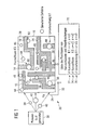
- Figure 1 shows a layout 10 of an integrated circuit with simulated defects.
- the layout 10 is through data described in a graphic format. This data is, for example the input data of a mask writer, with whose help generates the mask for producing the layout 10 becomes.
- the layout 10 contains dark layout structures 12 to 26, which are separated from one another by bright areas 28.
- the Data describe the location of the dark layout structures 12 to 26 with respect to a reference coordinate system 30, the one horizontal x-axis 32 and a vertical one y-axis has 34.
- the data also describe the shape the dark layout structures 12 to 26, in particular their Width in certain sections.
- the layout structures 12 to 26 are straight, i.e. they form or are rectangles angled 90 ° once or more. With others Other structures are simulated, e.g. spiral or curved structures. Due to the different structures of the dark layout structures 12 to 26 are the distances between adjacent layout structures 12 to 26 depending on the location.
- the random number generator 36 sorts the circles according to a given Poisson distribution at certain x, y positions.
- the circles 38 to 42 have diameters equal to the diameters of particles or structuring residues that correspond to the manufacturing to disturb.
- the Poisson distribution is specified such that the distribution of circles 38 to 42 on the layout 10 of the Distribution of particles of different sizes on one Wafer during the manufacturing process.
- a plurality of circles 44 to 68 are arranged simulate a highly exaggerated contamination. The biggest The diameter of the circles 44 to 68 corresponds approximately to the middle Width of the dark layout structures 12 to 26.
- Circles 44 through 68 are generated using the random number generator 36 arranged in a random manner. Also the selection of the The diameter of the circles is determined by a random function certainly. Circles 44 through 68 are represented by data in the graphics format that is also used to display the Layouts 10 is used. With those from image processing known methods can be determined at which points the circles 44 to 68 two dark line structures 12 to 26 connect, see for example circles 54 and 60, respectively the line structures 18 and 20 or the line structures 14 and 16 connect. According to the given simulation rules such a connection short-circuits , see short circuit K1 through circuit 60. In addition, with the help of methods known from image processing determines at which points circles 44 to 68 a layout structure 12 to 26 in two separate sections divide. This applies to circle 68, for example, which divides the layout structure 26. According to the rules for the error simulation are at the points determined in this way Interruptions recorded, see interruption U1 for the circle 68th
- Generated list 70 in which the positions of short circuits K1, K2 and interruptions U1 are noted.
- List 70 is in the method explained below with reference to Figures 2 and 3 used.
- the list 70 contains lines 72 to 76 in which a simulated error is noted in each case.
- For every short circuit K1, K2 and for each interruption U1 is one Local coordinate noted, see coordinate pairs x1, y1; x2, y2 or x3, y3.
- Figure 2 shows process steps for design improvement by Fault simulation.
- a method step 100 are made the defect monitoring of the production of integrated circuits so-called in-line data that generates the distribution of impurity particles with different diameters play. For example, runs through to determine this data a test disk the production. After going through this test disk is scanned with a laser beam and it becomes the number of particles with certain diameters determined. To determine the particles also use so-called differential image systems. With the help of In-line data then becomes the parameters for the random number generator 36, see arrow 102.
- the above using the Figure 1 explained simulation is based on the use a random generator 36 also as a Monte Carlo simulation referred to, see process step 104.
- layout data 106 that uses the layout the layers of the integrated circuit to be manufactured describe.
- Result of the Monte Carlo simulation in method step 104 is the list 70.
- a subsequent method step 108 is automatically with the help of a data processing system generates a ranking of the so-called "critical areas", these are areas in which the number of defects per area exceeds a predetermined threshold.
- the ranking list is in one Data processing system memory stored. Moreover the ranking list is printed out using a printer. Based on the ranking, the design of the layout improved, for example the dark layout structures in the "critical areas" with a greater distance from each other arranged.
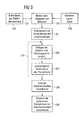
- Figure 3 shows method steps for testing integrated Circuits incorporating a fault simulation.
- Method step 120 corresponds to method step 100 and is used to determine the parameters for the random function, see arrow 122.
- the simulation step is carried out by a method step 124 shown.
- the Monte Carlo simulation in the procedural step 124 becomes layer layout data 126 of the one to be manufactured integrated circuit included.
- Result of Simulation in method step 124 is list 70 again, in which the positions of simulated short circuits K1, K2 and simulated interruptions U1 are noted.
- each in the List 70 noted bugs one affected by this bug Line or a component affected by this error determined automatically and / or manually. Subsequently is the model of the electrical for each error individually Circuit changed so that the circuit one by one Such an error affects the integrated circuit is reproduced. The changed circuit structure becomes generates an associated netlist.
- An analog step is then carried out in a method step 132 or digital resimulation with all test input vectors carried out.
- the resulting test result vectors are used for later testing of integrated circuits saved. Then the next one in list 70 noted errors considered, see arrow 134.
- Process steps 130 and 132 are carried out until to one for each error noted in list 70 Group of test result vectors has been generated. Is this the case follows immediately after method step 132 a process step 136 in which the groups of test result vectors with a group of target test output vectors be compared, the integrated working with a faultless Circuit would have to be generated. Groups of Test result vectors, in which deviations from the target output vectors occur are selected and for the saved later test. These test vectors are also called characteristic test vectors called because they are for one certain errors are characteristic, namely for the Error for which they were in steps 130 and 132 have been generated. It also becomes the groups of test result vectors the layout layer and the location of the error noted.
- step 138 are in a manufacturing process manufactured integrated circuits in an automatic Test facility checked. Deviations from test output vectors occur to the target test output vectors, so searched a database in which the characteristic Test result vectors are stored. Are the most characteristic Test result vectors for an error actually acquired test output vectors the same, so that for this Test result vectors noted layer and the position of the Error displayed on a display unit of the test facility and / or in an error file for later manual or automatic evaluation saved.
- the displayed Information is used to determine which production step used, in which the cause of the error must be searched, for example an improperly working filter unit for cleaning the surrounding medium in the relevant production room.
- Figure 4 shows the representation of the relationship between Yield and critical chip area in a coordinate system 150.
- a horizontal axis of abscissa 152 is used for illustration the critical chip area.
- a vertical axis of ordinates 154 is used to represent the yield in chip production, i.e. the ratio of functional integrated Circuits to the total number of integrated circuits on a semiconductor wafer.
- a curve 156 gives that Relationship between critical chip area and yield.
- the curve 156 has a course which is the course of a falling Corresponds to the exponential function.
- the location of curve 156 in coordinate system 150 is a function of that in the manufacturing process existing spatial density of the contaminants. With purer manufacturing conditions, curve 156 becomes higher yields shifted, see dashed curve 158. In the event of greater contamination in production curve 156 shifted towards smaller yields, see Dash-point curve 160.
- the critical chip area is the area per chip on which the Density of the errors determined with the Monte Carlo simulation exceeds a predetermined threshold value per unit area.
- a product PA with a small critical chip area has, for example, a yield of 98%, see cross 162.
- a product PB with a larger critical chip area than the product PA on the other hand, only has a yield of 94%.
- would on the abscissa axis 152, on the other hand, as usual Remove the total chip area of the products PA and PB for example, the total chip area of the product PA is larger than the total chip area of the product PB. The diminished Yield in the production of the product PB could be in not explain this case.
- the relationships shown in FIG. 4 are in another embodiment automatically on one Display unit shown to the designer of the layout when Support draft.
- the critical chip area is namely a particularly suitable one for improving the design Measure.
Landscapes
- Engineering & Computer Science (AREA)
- Physics & Mathematics (AREA)
- General Engineering & Computer Science (AREA)
- General Physics & Mathematics (AREA)
- Computer Hardware Design (AREA)
- Theoretical Computer Science (AREA)
- Evolutionary Computation (AREA)
- Geometry (AREA)
- Design And Manufacture Of Integrated Circuits (AREA)
Applications Claiming Priority (2)
| Application Number | Priority Date | Filing Date | Title |
|---|---|---|---|
| DE10105496 | 2001-02-07 | ||
| DE10105496 | 2001-02-07 |
Publications (2)
| Publication Number | Publication Date |
|---|---|
| EP1231551A2 true EP1231551A2 (fr) | 2002-08-14 |
| EP1231551A3 EP1231551A3 (fr) | 2005-09-07 |
Family
ID=7673139
Family Applications (1)
| Application Number | Title | Priority Date | Filing Date |
|---|---|---|---|
| EP02002387A Ceased EP1231551A3 (fr) | 2001-02-07 | 2002-01-31 | Procédé de simulation de défaut, qui peuvent se produire pendant le procédé de fabrication de semi-conducteurs et aussi de composants associés |
Country Status (1)
| Country | Link |
|---|---|
| EP (1) | EP1231551A3 (fr) |
Cited By (1)
| Publication number | Priority date | Publication date | Assignee | Title |
|---|---|---|---|---|
| FR2923021A1 (fr) * | 2007-10-26 | 2009-05-01 | Eads Europ Aeronautic Defence | Procede de determination de la sensibilite des composants electroniques vis-a-vis des particules. |
-
2002
- 2002-01-31 EP EP02002387A patent/EP1231551A3/fr not_active Ceased
Non-Patent Citations (5)
| Title |
|---|
| C. H. STAPPER: "Integrated circuit yield management and yield analysis: development and implementation", IEEE TRANSACTIONS ON SEMICONDUCTOR MANUFACTURING, vol. 8, no. 2, May 1995 (1995-05-01), pages 95 - 102 |
| G. A. ALLEN: "A Comparison of Efficient Dot Throwing and Shape Shifting Extra Material Critical Area Estimation", DEFECT AND FAULT TOLERANCE IN VLSI SYSTEMS, 1998, pages 44 - 52 |
| M. KATOOZI ET AL: "A BIST design of structured arrays with fault-tolerant layout", INTERNATIONAL TEST CONFERENCE 1988 PROCEEDING@M_NEW FRONTIERS IN TESTING, 1 January 1988 (1988-01-01), pages 514 - 521, XP055039119, ISBN: 978-0-81-860870-4, DOI: 10.1109/TEST.1988.207831 * |
| M. KATOOZI: "A BIST Design of structured arrays with fault tolerant layout", INTERNATIONAL TEST CONFERENCE, 1968 |
| S. FITZPATRICK ET AL.: "A Comparison of Critical Area Analysis Tools", IE-EE/SEMI ADVANCED SEMICONDUCTOR MANUFACTURING CONFERENCE, 1998, pages 31 - 33 |
Cited By (5)
| Publication number | Priority date | Publication date | Assignee | Title |
|---|---|---|---|---|
| FR2923021A1 (fr) * | 2007-10-26 | 2009-05-01 | Eads Europ Aeronautic Defence | Procede de determination de la sensibilite des composants electroniques vis-a-vis des particules. |
| WO2009056738A1 (fr) * | 2007-10-26 | 2009-05-07 | European Aeronautic Defence And Space Company Eads France | Procede de determination de la sensibilite des composants electroniques vis a vis des particules |
| CN101910855A (zh) * | 2007-10-26 | 2010-12-08 | 欧洲航空防务与空间公司Eads法国 | 确定电子部件对粒子的敏感度的方法 |
| US8577662B2 (en) | 2007-10-26 | 2013-11-05 | European Aeronautic Defence And Space Company Eads France | Method of determining the particle sensitivity of electronic components |
| CN101910855B (zh) * | 2007-10-26 | 2014-03-26 | 欧洲航空防务与空间公司Eads法国 | 确定电子部件对粒子的敏感度的方法 |
Also Published As
| Publication number | Publication date |
|---|---|
| EP1231551A3 (fr) | 2005-09-07 |
Similar Documents
| Publication | Publication Date | Title |
|---|---|---|
| DE60116769T2 (de) | Verfahren und system zur hierarchischen metallenden-, einschliessungs- und belichtungsprüfung | |
| DE69924296T2 (de) | Ic-test programmiersystem zur zuordnung logischer funktionstestdaten von logischen integrierten schaltung zu einer physikalischen darstellung | |
| DE3787431T2 (de) | Verfahren zur Generierung einer Kandidatenliste von fehlerhaften Schaltungselementen und Verfahren zur Isolierung von Fehlern in einer logischen Schaltung unter Verwendung dieser Kandidatenliste. | |
| DE112021000600T5 (de) | Fortschrittlicher inline part average test | |
| DE102015108244A1 (de) | Verfahren und system zum generieren eines schaltungsentwurfs, verfahren zum kalibrieren einer inspektionsvorrichtung, und verfahren zur prozesssteuerung und zum ertragsmanagement | |
| DE69520340T2 (de) | Apparat und Methode zur Chipausbeuteermittlung | |
| DE10047211A1 (de) | Verfahren und Messgerät zur Positionsbestimmung einer Kante eines Strukturelementes auf einem Substrat | |
| DE10036961B4 (de) | Verfahren zum Testen von Halbleiterwafern unter Verwendung von in Unterbereiche aufgeteilten Bereichen | |
| DE102019103503A1 (de) | Fehlerreduktion bei Bildern, die mit geladenen Teilchen erzeugt wurden, mithilfe von Machine-Learning-basierten Verfahren | |
| DE102004058753A1 (de) | Verifizierung von Integrierte-Schaltung-Tests unter Verwendung einer Testsimulation und einer Integrierte-Schaltungs-Simulation mit einem simulierten Ausfall | |
| DE102017215946A1 (de) | Prüfsystem, programm und steuerverfahren für prüfvorrichtung | |
| EP1134636A1 (fr) | Editeur de planification de processus | |
| DE102004008378A1 (de) | Optisches Nähenkorrekturverfahren | |
| DE102017117322A1 (de) | Verfahren zur Herstellung eines Halbleiterbauelementes mittels computergestütztem Entwurf von Testszenarien | |
| DE112009001219B4 (de) | Überprüfungsverfahren von Regeln von nicht-zu-untersuchenden Bereichen (DNIR), Computerprogramm und Vorrichtung für eine derartige Überprüfung | |
| DE10138142A1 (de) | Verfahren zur Analyse einer integrierten elektrischen Schaltung | |
| EP1231551A2 (fr) | Procédé de simulation de défaut, qui peuvent se produire pendant le procédé de fabrication de semi-conducteurs et aussi de composants associés | |
| DE10129654B4 (de) | Verfahren, Vorrichtung und Computerprogramm-Produkt zum Ermitteln von Auswirkungen von Konstruktionsänderungen | |
| DE10245452A1 (de) | Verfahren zum Bestimmen der Anordnung von Kontaktflächen auf der aktiven Oberseite eines Halbleiterchips | |
| DE102004003100A1 (de) | Verfahren zum Auflösen nicht richtig angepaßter graphischer Symbole bei einem rechnergestützten Entwurf integrierter Schaltungen | |
| DE102004019432A1 (de) | Verfahren und System zur virtuellen Inbetriebsetzung einer technischen Anlage mit bevorzugter Verwendung | |
| DE10325513B4 (de) | Verfahren und Vorrichtung zum Erstellen eines Verhaltensaspekts einer Schaltung zur formalen Verifikation | |
| DE10258164A1 (de) | Halbleitervorrichtungs-Analysesystem | |
| DE102021213650A1 (de) | Verfahren zum Verarbeiten von Geometriedaten, Computerprogrammprodukt sowie System zum Verarbeiten von Geometriedaten | |
| DE102017110065A1 (de) | Verfahren und Computerprogrammprodukt zur Modellierung eines NOx-Speicherverhaltens eines NOx-Speicherkatalysators |
Legal Events
| Date | Code | Title | Description |
|---|---|---|---|
| PUAI | Public reference made under article 153(3) epc to a published international application that has entered the european phase |
Free format text: ORIGINAL CODE: 0009012 |
|
| AK | Designated contracting states |
Kind code of ref document: A2 Designated state(s): AT BE CH CY DE DK ES FI FR GB GR IE IT LI LU MC NL PT SE TR |
|
| AX | Request for extension of the european patent |
Free format text: AL;LT;LV;MK;RO;SI |
|
| PUAL | Search report despatched |
Free format text: ORIGINAL CODE: 0009013 |
|
| AK | Designated contracting states |
Kind code of ref document: A3 Designated state(s): AT BE CH CY DE DK ES FI FR GB GR IE IT LI LU MC NL PT SE TR |
|
| AX | Request for extension of the european patent |
Extension state: AL LT LV MK RO SI |
|
| 17P | Request for examination filed |
Effective date: 20060109 |
|
| AKX | Designation fees paid |
Designated state(s): DE |
|
| 17Q | First examination report despatched |
Effective date: 20080514 |
|
| RAP1 | Party data changed (applicant data changed or rights of an application transferred) |
Owner name: INFINEON TECHNOLOGIES AG |
|
| STAA | Information on the status of an ep patent application or granted ep patent |
Free format text: STATUS: THE APPLICATION HAS BEEN REFUSED |
|
| 18R | Application refused |
Effective date: 20160414 |