EP1231712A2 - Amplificateur à gain variable - Google Patents
Amplificateur à gain variable Download PDFInfo
- Publication number
- EP1231712A2 EP1231712A2 EP02075529A EP02075529A EP1231712A2 EP 1231712 A2 EP1231712 A2 EP 1231712A2 EP 02075529 A EP02075529 A EP 02075529A EP 02075529 A EP02075529 A EP 02075529A EP 1231712 A2 EP1231712 A2 EP 1231712A2
- Authority
- EP
- European Patent Office
- Prior art keywords
- signal
- voltage
- input
- transistors
- amplifier
- Prior art date
- Legal status (The legal status is an assumption and is not a legal conclusion. Google has not performed a legal analysis and makes no representation as to the accuracy of the status listed.)
- Withdrawn
Links
Images


Classifications
-
- H—ELECTRICITY
- H03—ELECTRONIC CIRCUITRY
- H03G—CONTROL OF AMPLIFICATION
- H03G7/00—Volume compression or expansion in amplifiers
- H03G7/06—Volume compression or expansion in amplifiers having semiconductor devices
- H03G7/08—Volume compression or expansion in amplifiers having semiconductor devices incorporating negative feedback
Definitions
- the present invention relates to a variable gain amplifier, particularly to a radio frequency amplifier.
- Amplifier circuit structures the gain of which changes in response to the value of an applied control voltage are generally known.
- a circuit of such type is shown in Figure 1 where it is possible to distinguish three functional blocks: a voltage/current converter 10, a current divider 11 and a current/voltage conversion load 12.
- the current divider 11 is typically formed by two transistors Q10, Q20, for example bipolar transistors, in differential stage configuration, which have the emitter terminals connected with each other and coupled to the output of the block 10, the collector terminal of the transistor Q10 is connected with a supply voltage Vcc and the collector terminal of the transistor Q20 is connected with the block 12, while a control voltage Vc is applied at the base terminals of the transistors Q10 and Q20.
- the condition Vc>>Vt provides operatively to maintain the differential couple Q10, Q20 in high unbalance state, by making the greatest part of the signal current to pass through the electric path connected with the power supply Vcc.
- the load RL For increasing the gain in the applications wherein it is required, it is necessary to act on the load RL since the value of the transconductance Gm is fixed on the base of the distortion constraints of the signal; this causes a high reduction of the amplifier band of the amplifier and a high increasing of the thermal noise. Therefore the aforementioned circuit does not result applicable in the cases wherein high gains, high bandwidth and low noise are required.
- variable gain amplifier that overcomes at least in part the aforementioned limitations.
- variable gain amplifier comprising a first device to which a first control signal is applied so that the gain of an output signal of said first device with respect to a first input signal is a function of the exponential type of said first control signal, characterized by comprising a feedback network connected between an output terminal and an input terminal of said first device so as to assure that said gain in decibel of said first device is a linear function of said first control signal.
- variable gain amplifier that can be utilized in application requiring contemporaneously high gain, low noise and high bandwidth.
- the amplifier in Figure 2 comprises different functional blocks: a voltage/current converter 21 adapted to convert a voltage signal Vin into current, a current divider 22 and a current/voltage conversion load 23 adapted to converter an input current io into an output voltage Vo.
- the blocks 21, 22 and 23 are connected in series.
- the feedback network can be formed so that only the bias component is the utile information thereto.
- variable gain amplifier of Figure 2 wherein the feedback network 25 reacts only to the information of the bias current but acts combining both the components of bias and signal current at the node 24.
- the currents io and ir are sent to the respective blocks 31 and 32 which allow to extract the continuous component of the currents io and ir.
- Such blocks may be constituted by low pass filters or, in the case of differential structures, network sensitive only to the common mode signal.
- the continuous components of the current io and ir which output from the blocks 31 and 32, this is the current Io and Ir, are sent to the sum node 35; the current Ie given by Ie Io-Ir is sent to the input of a operational amplifier 33 able to generate an output voltage signal Vc2 proportional to the current Ie.
- the voltage signal Vc2 is sent to a voltage divider 34 where it is utilized as control signal and is applied at the base terminals of two npn bipolar transistors Q31 and Q32 arranged in differential configuration.
- the transistors Q31 and Q32 receive in input at the common emitter terminal the current i1 and the block 34 generates an output current ir sent in turn in input to the block 32 and to the sum node 24.
- the amplifier in Figure 3 does not react to the signal component and this allows to obtain a higher bandwidth of the amplifier.
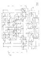
- FIG 4 an implementation circuit scheme of the structure shown in Figure 3 is described.
- the circuit structure shown is totally differential in order to make the circuit more immune to the disturbances.
- the block 21 comprises a first couple of npn bipolar transistor Q41, Q42 having the emitter terminals connected with each other and with a first current generator IEE, and a second couple of npn bipolar transistor Q43, Q44 having the emitter terminals connected with each other and with a second current generator IEE.
- the common emitter terminals of the transistor couples Q41, Q42 and Q43, Q44 are connected at the terminals of a resistor REE and a voltage signal Vin is applied between the base terminals of such transistor couples.
- the block 22 comprises a first couple of npn bipolar transistors Q45, Q46 arranged in differential configuration and which have the emitter terminals in common at the node C and are connected with the collector terminal of the transistor Q42, and a second couple of npn bipolar transistors Q47, Q48 arranged in differential configuration and which have the emitter terminals in common and are connected with the collector terminal of the transistor Q43.
- the control voltage Vc1 is applied at the base terminals in common of the transistors Q45, Q47 and of the transistors Q45, Q48 and a bias voltage Vbias2 is applied only at the base terminals in common of the transistors Q45, Q48.
- the collector terminals of the transistors Q46, Q47 are connected with the supply voltage Vcc while the collector terminals of the transistors Q45 and Q48 are connected with two resistors Rc1 connected both with the supply voltage Vcc and which form the block 23.
- the collector terminals of the transistors Q45 and Q48 are the output terminals Out1 and Out2 of the amplifier and are connected with two resistors Rb which have the other terminal B in common.
- the block 25 comprises a first transistor group constituted by couples of npn bipolar transistors Q51, Q52 and Q53, Q54 arranged in differential configuration and a second transistor group constituted by couples of npn bipolar transistors Q55, Q56 and Q57, Q58 arranged in differential configuration.
- the emitter terminals in common of the first group are connected at node D with the collector terminal of the transistor Q41 while the emitter terminals in common of the second group are connected with the collector terminal of the transistor Q44.
- the base terminals of the transistors Q51, Q52 and Q57, Q58 are connected with a bias voltage generator Vbias1 and the collector terminals are connected with the supply voltage Vcc.
- the collector terminals of the transistors Q54 and Q55 are connected respectively with the collector terminals of the transistors Q42 and Q43 while the collector terminals of the transistors Q53 and Q56 are connected with respective resistors Rc2 connected with the supply voltage Vcc and are connected with respective resistors Ra having a terminal A in common.
- the terminals A and B are the input terminals of the operational amplifier 33, respectively the not inverting input and the inverting input.
- the output terminal of the operational amplifier 33 is connected with the common base terminals of the transistors Q53, Q54 and Q55, Q56.
- the operational amplifier 33 detects a common mode voltage Vm by means of the terminal B and, for the feedback, generates in output the voltage Vc2 so that the voltage at the terminal A is next the voltage at the terminal B.
- n is the rate between the resistors Rc2 and Rc1 which is equal to the rate of the areas of the transistors Q51-Q52, Q54-Q53, Q55-Q56, Q58-Q57.
- i 45 i 54+ i 42 1+exp( Vc 1/ Vt )
- i 54 n n +1 * i 41 1+exp( Vc 2/ Vt )
- the amplifier in Figure 4 is not sensitive to eventual offsets of the operational amplifier 33; in fact when the gain Av is low, this is when the offset of the operational amplifier 33 has a greater weight because it becomes similar to the voltage Vout of the load, the correction effect of the reaction with respect to the linearitation of the gain curve is negligible because with Vc1>>Vt it is obtained that 1+exp(Vc1/Vt) ⁇ exp(Vc1/Vt).
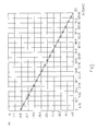
- FIG 5 a diagram of the voltage gain Av (in decibel) of the amplifier in Figure 4 in function of the control voltage Vc1 is shown in the case wherein the amplifier has a gain range of 40 dB, a maximum gain of 0 dB, a linearity accuracy of the gain curve of 1 dB.
- transistors MOS may be utilized alternatively.
Landscapes
- Control Of Amplification And Gain Control (AREA)
- Ultra Sonic Daignosis Equipment (AREA)
- Amplifiers (AREA)
Applications Claiming Priority (2)
| Application Number | Priority Date | Filing Date | Title |
|---|---|---|---|
| ITMI010284 | 2001-02-13 | ||
| IT2001MI000284A ITMI20010284A1 (it) | 2001-02-13 | 2001-02-13 | Amplificatore a guadagno variabile |
Publications (2)
| Publication Number | Publication Date |
|---|---|
| EP1231712A2 true EP1231712A2 (fr) | 2002-08-14 |
| EP1231712A3 EP1231712A3 (fr) | 2004-04-28 |
Family
ID=11446848
Family Applications (1)
| Application Number | Title | Priority Date | Filing Date |
|---|---|---|---|
| EP02075529A Withdrawn EP1231712A3 (fr) | 2001-02-13 | 2002-02-07 | Amplificateur à gain variable |
Country Status (3)
| Country | Link |
|---|---|
| US (1) | US6661286B2 (fr) |
| EP (1) | EP1231712A3 (fr) |
| IT (1) | ITMI20010284A1 (fr) |
Families Citing this family (5)
| Publication number | Priority date | Publication date | Assignee | Title |
|---|---|---|---|---|
| US6906592B2 (en) | 2002-11-13 | 2005-06-14 | Qualcomm Inc | Continuously variable gain radio frequency driver amplifier having linear in decibel gain control characteristics |
| TW200505157A (en) * | 2003-07-21 | 2005-02-01 | Realtek Semiconductor Corp | Linear-in-decibel variable gain amplifier |
| KR100703710B1 (ko) * | 2005-06-29 | 2007-04-06 | 삼성전자주식회사 | Dc출력 오프셋을 제거할 수 있는 장치 및 방법 |
| WO2011100358A2 (fr) * | 2010-02-09 | 2011-08-18 | Fabrico Technology, Inc. | Systèmes et procédés pour détecter des analytes cibles |
| RU2421887C1 (ru) * | 2010-05-27 | 2011-06-20 | Государственное образовательное учреждение высшего профессионального образования "Южно-Российский государственный университет экономики и сервиса" (ГОУ ВПО "ЮРГУЭС") | Дифференциальный усилитель с парафазным выходом |
Family Cites Families (4)
| Publication number | Priority date | Publication date | Assignee | Title |
|---|---|---|---|---|
| GB1546672A (en) * | 1975-07-03 | 1979-05-31 | Sony Corp | Signal compression and expansion circuits |
| DE3204217A1 (de) * | 1982-02-08 | 1983-08-18 | Philips Patentverwaltung Gmbh, 2000 Hamburg | Schaltung zur elektronischen verstaerkungsstellung |
| FR2672750B1 (fr) * | 1991-02-08 | 1996-12-20 | Thomson Composants Militaires | Circuit d'amplification a commande de gain exponentielle. |
| US5528197A (en) * | 1995-06-06 | 1996-06-18 | Analog Devices, Inc. | Voltage controlled amplifier |
-
2001
- 2001-02-13 IT IT2001MI000284A patent/ITMI20010284A1/it unknown
-
2002
- 2002-02-07 EP EP02075529A patent/EP1231712A3/fr not_active Withdrawn
- 2002-02-13 US US10/075,161 patent/US6661286B2/en not_active Expired - Lifetime
Also Published As
| Publication number | Publication date |
|---|---|
| US20020140507A1 (en) | 2002-10-03 |
| US6661286B2 (en) | 2003-12-09 |
| ITMI20010284A1 (it) | 2002-08-13 |
| EP1231712A3 (fr) | 2004-04-28 |
Similar Documents
| Publication | Publication Date | Title |
|---|---|---|
| US6690232B2 (en) | Variable gain amplifier | |
| US5917383A (en) | Compact voltage controlled ring oscillator with quadrature outputs | |
| EP0500694A1 (fr) | Amplificateur de puissance cmos entierement differentiel. | |
| US4267519A (en) | Operational transconductance amplifiers with non-linear component current amplifiers | |
| KR100491390B1 (ko) | 능동 위상 분할기 | |
| JPS63283307A (ja) | 信号変換回路 | |
| US4331929A (en) | Gain-controlled amplifier | |
| US4835487A (en) | MOS voltage to current converter | |
| KR0134178B1 (ko) | 개량된 선형성을 갖는 트랜스콘덕턴스 셀 | |
| EP0196906A2 (fr) | Circuit de détection d'un signal de commande de gain automatique | |
| US6236268B1 (en) | High-gain amplifier having a limited output dynamic range | |
| EP0242479A2 (fr) | Atténuateur de précision commuté à distance | |
| EP1231712A2 (fr) | Amplificateur à gain variable | |
| US6531920B1 (en) | Differential amplifier circuit | |
| US20080143441A1 (en) | Amplifier having plurality of differential pairs and communication system equipped with same | |
| EP0410295B1 (fr) | Hacheur-amplificateur opérationnel du type push-pull à sortie unique | |
| US4825104A (en) | Comparator | |
| JP3081210B2 (ja) | 線形利得増幅回路 | |
| US20040066232A1 (en) | Variable-gain differential input and output amplifier | |
| EP0589676B1 (fr) | Circuit de conversion variable de tension en courant | |
| US5566365A (en) | Active filter circuit and portable telephone apparatus | |
| US5576646A (en) | Transconductor circuit with high-linearity double input and active filter thereof | |
| US5767662A (en) | Amplifier having single-ended input and differential output and method for amplifying a signal | |
| US4064463A (en) | Amplifier circuit | |
| JPH07142941A (ja) | 増幅器出力段 |
Legal Events
| Date | Code | Title | Description |
|---|---|---|---|
| PUAI | Public reference made under article 153(3) epc to a published international application that has entered the european phase |
Free format text: ORIGINAL CODE: 0009012 |
|
| AK | Designated contracting states |
Kind code of ref document: A2 Designated state(s): AT BE CH CY DE DK ES FI FR GB GR IE IT LI LU MC NL PT SE TR |
|
| AX | Request for extension of the european patent |
Free format text: AL;LT;LV;MK;RO;SI |
|
| PUAL | Search report despatched |
Free format text: ORIGINAL CODE: 0009013 |
|
| AK | Designated contracting states |
Kind code of ref document: A3 Designated state(s): AT BE CH CY DE DK ES FI FR GB GR IE IT LI LU MC NL PT SE TR |
|
| AX | Request for extension of the european patent |
Extension state: AL LT LV MK RO SI |
|
| 17P | Request for examination filed |
Effective date: 20041019 |
|
| AKX | Designation fees paid |
Designated state(s): DE FR GB IT |
|
| 17Q | First examination report despatched |
Effective date: 20050131 |
|
| STAA | Information on the status of an ep patent application or granted ep patent |
Free format text: STATUS: THE APPLICATION IS DEEMED TO BE WITHDRAWN |
|
| 18D | Application deemed to be withdrawn |
Effective date: 20080902 |