EP1232407B1 - Wärmeabsorbierender filter und verfahren zu dessen herstellung - Google Patents
Wärmeabsorbierender filter und verfahren zu dessen herstellung Download PDFInfo
- Publication number
- EP1232407B1 EP1232407B1 EP00988872A EP00988872A EP1232407B1 EP 1232407 B1 EP1232407 B1 EP 1232407B1 EP 00988872 A EP00988872 A EP 00988872A EP 00988872 A EP00988872 A EP 00988872A EP 1232407 B1 EP1232407 B1 EP 1232407B1
- Authority
- EP
- European Patent Office
- Prior art keywords
- sio
- tio
- filter
- layer
- substrate
- Prior art date
- Legal status (The legal status is an assumption and is not a legal conclusion. Google has not performed a legal analysis and makes no representation as to the accuracy of the status listed.)
- Expired - Lifetime
Links
- 238000000034 method Methods 0.000 title claims abstract description 26
- 239000000463 material Substances 0.000 claims abstract description 68
- 239000000758 substrate Substances 0.000 claims abstract description 53
- 239000011248 coating agent Substances 0.000 claims abstract description 26
- 238000000576 coating method Methods 0.000 claims abstract description 26
- 230000008021 deposition Effects 0.000 claims abstract description 25
- 238000004519 manufacturing process Methods 0.000 claims abstract description 11
- 230000008569 process Effects 0.000 claims abstract description 11
- 230000005540 biological transmission Effects 0.000 claims description 69
- VYPSYNLAJGMNEJ-UHFFFAOYSA-N Silicium dioxide Chemical compound O=[Si]=O VYPSYNLAJGMNEJ-UHFFFAOYSA-N 0.000 claims description 53
- 239000011521 glass Substances 0.000 claims description 38
- 238000000151 deposition Methods 0.000 claims description 34
- 230000003287 optical effect Effects 0.000 claims description 29
- 238000001704 evaporation Methods 0.000 claims description 25
- 230000008020 evaporation Effects 0.000 claims description 25
- PJXISJQVUVHSOJ-UHFFFAOYSA-N indium(iii) oxide Chemical compound [O-2].[O-2].[O-2].[In+3].[In+3] PJXISJQVUVHSOJ-UHFFFAOYSA-N 0.000 claims description 10
- 229910003437 indium oxide Inorganic materials 0.000 claims description 9
- 238000004544 sputter deposition Methods 0.000 claims description 8
- 238000000137 annealing Methods 0.000 claims description 7
- ATJFFYVFTNAWJD-UHFFFAOYSA-N Tin Chemical compound [Sn] ATJFFYVFTNAWJD-UHFFFAOYSA-N 0.000 claims description 6
- 239000000203 mixture Substances 0.000 claims description 4
- 239000004033 plastic Substances 0.000 claims description 3
- XOLBLPGZBRYERU-UHFFFAOYSA-N tin dioxide Chemical compound O=[Sn]=O XOLBLPGZBRYERU-UHFFFAOYSA-N 0.000 claims description 3
- 229910001887 tin oxide Inorganic materials 0.000 claims description 3
- 239000012298 atmosphere Substances 0.000 claims description 2
- 229910052739 hydrogen Inorganic materials 0.000 claims description 2
- 229910052757 nitrogen Inorganic materials 0.000 claims description 2
- 238000007738 vacuum evaporation Methods 0.000 claims description 2
- GWEVSGVZZGPLCZ-UHFFFAOYSA-N Titan oxide Chemical compound O=[Ti]=O GWEVSGVZZGPLCZ-UHFFFAOYSA-N 0.000 claims 42
- 229910052681 coesite Inorganic materials 0.000 claims 25
- 229910052906 cristobalite Inorganic materials 0.000 claims 25
- 239000000377 silicon dioxide Substances 0.000 claims 25
- 229910052682 stishovite Inorganic materials 0.000 claims 25
- 229910052905 tridymite Inorganic materials 0.000 claims 25
- 229910052581 Si3N4 Inorganic materials 0.000 claims 1
- 239000013307 optical fiber Substances 0.000 claims 1
- 230000005855 radiation Effects 0.000 abstract description 10
- 239000010410 layer Substances 0.000 description 78
- 229910004298 SiO 2 Inorganic materials 0.000 description 52
- 229910010413 TiO 2 Inorganic materials 0.000 description 41
- 238000001228 spectrum Methods 0.000 description 31
- 239000010408 film Substances 0.000 description 26
- 238000010521 absorption reaction Methods 0.000 description 11
- 238000009877 rendering Methods 0.000 description 11
- 229910052760 oxygen Inorganic materials 0.000 description 10
- 239000001301 oxygen Substances 0.000 description 10
- 238000000411 transmission spectrum Methods 0.000 description 10
- QVGXLLKOCUKJST-UHFFFAOYSA-N atomic oxygen Chemical compound [O] QVGXLLKOCUKJST-UHFFFAOYSA-N 0.000 description 9
- 150000002500 ions Chemical class 0.000 description 9
- 230000006870 function Effects 0.000 description 8
- 238000000572 ellipsometry Methods 0.000 description 7
- 230000000694 effects Effects 0.000 description 6
- 230000003595 spectral effect Effects 0.000 description 6
- XKRFYHLGVUSROY-UHFFFAOYSA-N argon Substances [Ar] XKRFYHLGVUSROY-UHFFFAOYSA-N 0.000 description 5
- 239000003989 dielectric material Substances 0.000 description 5
- 238000001914 filtration Methods 0.000 description 4
- 229910052751 metal Inorganic materials 0.000 description 4
- 239000002184 metal Substances 0.000 description 4
- 238000011282 treatment Methods 0.000 description 4
- 229910052786 argon Inorganic materials 0.000 description 3
- 238000012512 characterization method Methods 0.000 description 3
- 239000003086 colorant Substances 0.000 description 3
- 230000007423 decrease Effects 0.000 description 3
- -1 gold Chemical class 0.000 description 3
- 238000001755 magnetron sputter deposition Methods 0.000 description 3
- 238000005259 measurement Methods 0.000 description 3
- 150000002739 metals Chemical class 0.000 description 3
- 241000894007 species Species 0.000 description 3
- 239000000969 carrier Substances 0.000 description 2
- 230000008859 change Effects 0.000 description 2
- 239000006185 dispersion Substances 0.000 description 2
- 239000000835 fiber Substances 0.000 description 2
- 238000010438 heat treatment Methods 0.000 description 2
- 230000006872 improvement Effects 0.000 description 2
- 238000011065 in-situ storage Methods 0.000 description 2
- 238000005457 optimization Methods 0.000 description 2
- 230000009467 reduction Effects 0.000 description 2
- 229910052710 silicon Inorganic materials 0.000 description 2
- 239000010703 silicon Substances 0.000 description 2
- 229910052814 silicon oxide Inorganic materials 0.000 description 2
- 239000002356 single layer Substances 0.000 description 2
- 239000010409 thin film Substances 0.000 description 2
- 230000007704 transition Effects 0.000 description 2
- 238000001429 visible spectrum Methods 0.000 description 2
- RTAQQCXQSZGOHL-UHFFFAOYSA-N Titanium Chemical compound [Ti] RTAQQCXQSZGOHL-UHFFFAOYSA-N 0.000 description 1
- 230000002745 absorbent Effects 0.000 description 1
- 239000002250 absorbent Substances 0.000 description 1
- 230000001464 adherent effect Effects 0.000 description 1
- 229910052782 aluminium Inorganic materials 0.000 description 1
- XAGFODPZIPBFFR-UHFFFAOYSA-N aluminium Chemical compound [Al] XAGFODPZIPBFFR-UHFFFAOYSA-N 0.000 description 1
- 230000003667 anti-reflective effect Effects 0.000 description 1
- 230000008033 biological extinction Effects 0.000 description 1
- 229910052799 carbon Inorganic materials 0.000 description 1
- 150000001875 compounds Chemical class 0.000 description 1
- 238000005520 cutting process Methods 0.000 description 1
- 230000003247 decreasing effect Effects 0.000 description 1
- 230000007547 defect Effects 0.000 description 1
- 238000005137 deposition process Methods 0.000 description 1
- 230000001066 destructive effect Effects 0.000 description 1
- 238000010586 diagram Methods 0.000 description 1
- 230000008030 elimination Effects 0.000 description 1
- 238000003379 elimination reaction Methods 0.000 description 1
- 238000000295 emission spectrum Methods 0.000 description 1
- 230000003628 erosive effect Effects 0.000 description 1
- 238000002474 experimental method Methods 0.000 description 1
- 239000007789 gas Substances 0.000 description 1
- PCHJSUWPFVWCPO-UHFFFAOYSA-N gold Chemical compound [Au] PCHJSUWPFVWCPO-UHFFFAOYSA-N 0.000 description 1
- 239000010931 gold Substances 0.000 description 1
- 229910052737 gold Inorganic materials 0.000 description 1
- 229910052736 halogen Inorganic materials 0.000 description 1
- 150000002367 halogens Chemical class 0.000 description 1
- 229910052738 indium Inorganic materials 0.000 description 1
- APFVFJFRJDLVQX-UHFFFAOYSA-N indium atom Chemical compound [In] APFVFJFRJDLVQX-UHFFFAOYSA-N 0.000 description 1
- 238000010884 ion-beam technique Methods 0.000 description 1
- 230000001678 irradiating effect Effects 0.000 description 1
- 230000000670 limiting effect Effects 0.000 description 1
- 238000011326 mechanical measurement Methods 0.000 description 1
- 229910044991 metal oxide Inorganic materials 0.000 description 1
- 150000004706 metal oxides Chemical class 0.000 description 1
- 230000007935 neutral effect Effects 0.000 description 1
- 150000004767 nitrides Chemical class 0.000 description 1
- 239000012299 nitrogen atmosphere Substances 0.000 description 1
- 230000010355 oscillation Effects 0.000 description 1
- 238000013021 overheating Methods 0.000 description 1
- 230000036961 partial effect Effects 0.000 description 1
- 230000037361 pathway Effects 0.000 description 1
- 230000008447 perception Effects 0.000 description 1
- 230000010363 phase shift Effects 0.000 description 1
- 239000004417 polycarbonate Substances 0.000 description 1
- 229920000515 polycarbonate Polymers 0.000 description 1
- 239000010453 quartz Substances 0.000 description 1
- 230000002829 reductive effect Effects 0.000 description 1
- 230000004044 response Effects 0.000 description 1
- 230000035945 sensitivity Effects 0.000 description 1
- 238000000391 spectroscopic ellipsometry Methods 0.000 description 1
- 238000005507 spraying Methods 0.000 description 1
- 239000000126 substance Substances 0.000 description 1
- 238000010408 sweeping Methods 0.000 description 1
- 239000013077 target material Substances 0.000 description 1
- 238000012360 testing method Methods 0.000 description 1
- 239000010936 titanium Substances 0.000 description 1
- 229910052719 titanium Inorganic materials 0.000 description 1
Images




Classifications
-
- C—CHEMISTRY; METALLURGY
- C03—GLASS; MINERAL OR SLAG WOOL
- C03C—CHEMICAL COMPOSITION OF GLASSES, GLAZES OR VITREOUS ENAMELS; SURFACE TREATMENT OF GLASS; SURFACE TREATMENT OF FIBRES OR FILAMENTS MADE FROM GLASS, MINERALS OR SLAGS; JOINING GLASS TO GLASS OR OTHER MATERIALS
- C03C17/00—Surface treatment of glass, not in the form of fibres or filaments, by coating
- C03C17/34—Surface treatment of glass, not in the form of fibres or filaments, by coating with at least two coatings having different compositions
- C03C17/3411—Surface treatment of glass, not in the form of fibres or filaments, by coating with at least two coatings having different compositions with at least two coatings of inorganic materials
- C03C17/3417—Surface treatment of glass, not in the form of fibres or filaments, by coating with at least two coatings having different compositions with at least two coatings of inorganic materials all coatings being oxide coatings
Definitions
- the present invention relates to a filter anticaloric and to a process for the manufacture of filtered.
- An energy-absorbing filter may for example be used to filter a compound operative light a light source that emits energy, or radiation, in the visible and infrared domains. It must make it possible to filter the light emitted by this source so as to prevent infrared radiation from hinders the surgical team or the patient.
- This filter must block the longest lengths while remaining neutral in the sense of the perception of colors by the human eye in the visible domain.
- the lowest wavelengths can also be absorbed or reflected by the filtered.
- such a filter can also be used for a care lamp, a office lamp, a fiber lighting system optical, glazing, optical projection system, a light bulb, etc ...
- this type of filter is made from an opaque doped glass at infrared radiation.
- the transmission spectrum of this doped glass for a thickness of 3 mm is proposed in FIG. annex, referenced 1, and compared with the spectrum of transmission of an ordinary glass 3 mm thick, referenced 3.
- the y-axis represents the internal transmission T and the axis of abscissa, the wavelength ⁇ in nm.
- a multilayer treatment of this doped glass intended to deposit layers of SiO 2 and Nb 2 O 5 makes it possible to improve its transmission in the visible range to make an anticaloric filter, hereinafter referred to as a doped glass filter.
- the optical performances of this filter are given in Table 1 below: Definition Doped glass filter Energy radian RE (mW / m 2 / Lux) 4.25 Visible average transmission T screw (%) 80.4 Color temperature T coul (K) 3585 IRC or R A color rendering index (CIE standards ) 97.3 R 9 (CIE standards ) 84.4
- the doped glass filter is an expensive material that does not work well in a humid and hot environment. For example in countries with a tropical climate, it is necessary to protect this filter from moisture and UV with an additional layer of SiO 2 , which increases its manufacturing cost.
- GB-A-2324098 discloses an anticaloric filter comprising a glass substrate, a layer of an infrared reflective material, a coating forming an interference filter which comprises a stacking group of a first and a second film of refractive index n 1 and n 2 repeated N times.
- US-A-5341238 discloses a filter anticaloric which comprises, a substrate, a layer of ITO a multilayer interference filter and a second interference filter.
- the second filter is designed to reflect radiation in a band visible narrow, for example the radiation of a laser HeNe.
- the present invention is specifically intended to overcome the aforementioned drawbacks by providing a low cost manufacturing heat filter having the required properties in the visible or visible spectrum domain and in the domain infrared.
- This heat absorbing filter comprises a substrate, at least one layer of an infrared reflective material, and a coating forming an interference filter in the visible domain.
- the present invention provides a anticaloric filter comprising a substrate, a layer an infrared reflective material covering at least a surface of the substrate, and a coating forming a interference filter in the visible range covering said layer of reflective material infrared.
- the substrate may be a glass substrate, such only clear transparent glass, or plastic.
- the glass substrate has, for example, for a thickness of 2 mm, a transparency of 30% to about 3 microns.
- the substrate is plastic
- the infrared reflective material can be a transparent conductive oxide, for example oxide of indium doped with tin (ITO).
- ITO indium doped with tin
- transparent conductive oxide By varying the chemical composition of transparent conductive oxide, it is possible to change the level of infrared reflection and the transition wavelength between a behavior dielectric, that is to say transparent and metallic, that is to say, reflector. This is the case for example for ITO.
- indium oxide doped with tin can report Sn / In ranging from about 9 to about 11% by weight, for example about 10% by weight mass. A ratio of approximately 10% by weight allows to obtain a maximum level of reflection.
- reflective materials may be used, for example metals such as gold, money or aluminum. But they are also reflectors in the visible, so it is necessary to deposit them in very thin layers, for example About 10 nm, to preserve a transmission sufficient.
- the coating forming a interference filter in the visible range may comprise at least one stacking group repeated N times of at least a first film and at least a second film, wherein said stacking group has an alternation of the first film and the second film, the first film having a thickness L or multiple of L and consisting of a first material having a refractive index n 1 , and the second film having a thickness H or multiple of H and being made of a second material having a refractive index n 2 , wherein N is an integer and H and L are geometric thicknesses, and wherein N, H, L, n 1 and n 2 are such that the
- the interference filter coating has a transmission window between 400 and 800 nm.
- the definition of the geometric thickness is given by considering a film or a thin layer deposited on any substrate and a reference wavelength ⁇ 0 .
- This layer of thickness has an index of value n for this reference wavelength. If the layer is illuminated with a source I 0 of wavelength ⁇ 0 , the portion of the light radiation I 1 reflected at the first interface, that is to say the air-layer interface, will interfere with that I 2 reflected at the second interface, that is to say at the interface layer-substrate as shown in Figure 16 in the appendix.
- the phase shift of the wave I 2 with respect to the wave I 1 comes from the passage through the layer and is 4 ⁇ ne / ⁇ 0 cos ⁇ . If it is equal to (2p + 1) ⁇ , with p integer, and insofar as the value of the index of the substrate is lower than that of the index of the layer deposited, the interferences are destructive and the reflection is minimal at ⁇ 0 .
- the layer is called quarter-wave layer and is denoted H if the index is strong, L if the index is weak.
- ⁇ is the angle made by the refracted ray in the medium of index n. In general, we work at normal incidence, cos ⁇ is 1.
- the architecture of a stack is, in general, given in multiples of films or quarter-wave layers, this is called geometrical thickness.
- the interest of such a notation is to be able to shift spectrally the properties of the stack in not changing that the value of the wavelength of reference, insofar as the index n is constant between the two wavelengths.
- the first material may be SiO 2 and the second material may be TiO 2 .
- the first material may be SiO 2 and the second material Si 3 N 4 . Any other pair of materials having dielectric behavior and different index values is acceptable.
- the coating forming a interference filter in the visible range may comprise a first stacking group having an alternation of 0.5L / H / 0.5L type repeated 8 times.
- it may comprise a second stacking group having an alternation of the type 0.65L / 1.3H / 0.65L repeated 8 times.
- the substrate may be a glass substrate
- the transparent conductive oxide layer may be a tin-doped indium oxide layer
- the interference-filter-forming coating in the field visible can be a stack in which alternate films of SiO 2 and TiO 2 films, the stack starting with a film of SiO 2 deposited on the ITO layer and ending with a TiO 2 film in contact with the atmosphere, said stack comprising 17 films of SiO 2 and 16 films of TiO 2 .
- the coating forming a interference filter in the visible range comprises a first stacking group having an alternation of 0.5L / H / 0.5L type repeated 6 times . It may further comprise a second stacking group having a alternation of 0.65L / 1.3H / 0.65L type repeated 6 times.
- the heat-absorbing filter may furthermore comprise an anti-reflective layer and / or an anti-scratch layer.
- the filter of the present invention can be used for example in an optical system such as a surgical lighting, a care lamp, a lamp, a desk lamp, a fiber lighting system optical, glazing, optical projection system, a bulb, etc.
- the present invention relates to therefore also to such a system comprising a filter according to that of the present invention, for example operating light or treatment lamp, for example example of medical, aesthetic, etc.
- the light source can be for example a filament bulb, a halogen lamp, a lamp incandescence, etc ...
- the present invention also relates to a method of manufacturing an energy-absorbing filter comprising a substrate, at least one layer of a infrared reflective material and a coating forming an interference filter in the visible range.
- the infrared reflective material is tin-doped indium oxide (ITO)
- this material can be deposited by magnetron sputtering onto the substrate, for example from a sintered target whose composition is from about 9 to about 11% by weight, for example about 10% by weight of tin oxide in In 2 O 3 .
- the method of the invention may further comprise a step 1 ) of annealing the infrared reflective material deposited on the substrate.
- step c) of deposition of the interference filter can be a film deposition step performed by a vacuum evaporation or sputtering technique.
- Evaporation under vacuum can be carried out by example by means of an electron gun.
- This device consists of deflecting a beam of electrons emitted by a filament in a crucible containing the material to be drop.
- the target material evaporates and condenses on a substrate placed next to the crucible. This method allows to deposit different types of materials such as oxides and metals.
- the electron gun can be for example the Model EVA 1200 (Trademark) of the Company Alliance Concept, FRANCE.
- the layers In the case of oxides, it may be necessary to add oxygen to the enclosure to improve the stoichiometry of the layers.
- the low working pressure of the order of 10 -2 to 10 -3 Pa allows the deposition of thin film of high purity.
- the energy of the evaporated species being less than 1 eV, that is to say relatively low, the layers often have a columnar structure and are low density and little adherent.
- This ionic assistance can be reactive for example when using oxygen ions, or non reactive by example when using argon ions.
- the different deposition parameters such as energy, temperature, partial pressures, flow or nature of ions help optimize properties optical layers deposited.
- Sputtering as for it consists to make an electric discharge in a gaseous medium with a rare or reactive gas, between the cathode constituted by material to be deposited and the electrode to ground the most close.
- the ions of the plasma generated bombard the target, and the pulverized species condense on the substrate.
- Magnetron sputtering is a high energy deposition process for species sprayed (some eV).
- the adhesion of the layers deposited is often greater than that observed in the case of evaporation.
- the pressure of work in the enclosure is higher, of the order of 0.1 to 1 Pa, which can generate a certain rate of pollution in the layers.
- the structure of the films depends mainly on the pressure and target-substrate distance.
- the oxide deposit requires either to work in radiofrequency, that is to say around 13.56 MHz, either in direct current DC on a metal target in reactive medium.
- the deposition temperature is higher than in DC, of the order of 80 ° C and the speed deposit is slower.
- Sputtering or spraying cathodic magnetron can be achieved for example at means of a sputtering machine magnetron type BAK 550 (trademark) of the Balzers Company, LICHTENSTEIN.
- the interference filter when the interference filter comprises at least one stacking group repeated N times as defined above, in which the first material is SiO 2 and in which the second material is Si 3 N 4 , the deposition step the interference filter may be a film deposition step performed by a plasma deposition technique.
- the present invention lies in particular in the combination of an infrared filter and a UV-Visible filter, can be deposited on a glass substrate ordinary, as well as in the level of performance of this filter.
- the filter of the present invention makes it possible filter the infrared radiation from a lighting such than an incandescent lamp without disturbing vision colors by the human eye.
- the filter also offers a transmission important in the visible spectral domain. It allows avoid overheating of the observation area and guarantee a good vision of colors and a good light output power / power output electric.
- the inventors have at first, separated the two spectral domains. They present below, the process that leads to defining the architecture of a purely dielectric stack to form the coating forming the interference filter in the visible domain.
- Table 2 summarizes the various deposition techniques that were tested for each monolayer (SiO 2 and TiO 2 ). Summary of the different deposit methods studied Evaporation Gaseous sweeping Ionic assistance Nature of assistance 1 Simple no no - 2 reactive oxygen no - 3 assisted no Yes argon 4 Reactive assisted oxygen Yes argon 5 Reactive Assisted no Yes oxygen 6 Reactive assisted reactive oxygen Yes oxygen
- optical properties of each SiO 2 or TiO 2 unit layer were determined by UV-Visible-near IR spectroscopic ellipsometry.
- the layers measured were deposited on silicon.
- the silicon is not optimal in the visible range because it is difficult, at short wavelengths, to to separate the absorption due to the layer from that due to substrate, its optical properties are well known, and its opacity in the visible range makes it possible not to be bothered by the reflections on the back side of the substrate.
- n A not + B not ⁇ -2 + C not ⁇ -4
- n n constant at high wavelengths and a significant increase in this value when the wavelength decreases, that is to say that the frequencies by increasing close to the value of the "gap", corresponding to the bandgap energy.
- the model of the Urbach's tail for k decreasing exponentially from UV to longer wavelengths can be used.
- the coefficient 1240 comes from the fact that inventors worked in nm while the phenomenon is physically described in energy unit (eV).
- the deposit technique chosen is the one that allows to obtain the optical characteristics of each material approximating those of materials massive, with the highest index contrast observable between the two oxides.
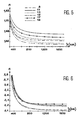
- the abscissa axis indicates the wavelength ⁇ in nm
- the ordinate axis indicates the refractive index n of the material
- Figure 5 was made with SiO 2 and Figure 6 with TiO 2 .
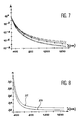
- the legend shown in Figure 5 is also valid for Figures 6 and 7.
- Reference 9 indicates a simple evaporation, the reference 11 assisted evaporation, reference 13 a reactive evaporation, the reference 15 a reactive evaporation assisted, the reference 17 a reactive assisted evaporation and the reference 19 a reactive assisted reactive evaporation.
- the value of the absorption coefficient k of SiO 2 is not measurable by ellipsometry because it is less than 10 -3 .
- k SiO 2 0 has been set.
- the refractive index of SiO 2 varies little according to the deposition conditions: at 600 nm, it varies from 1.46 to 1.485.
- n the lowest values of n and the closest to those of the massive material are obtained in the case of simple evaporation, assisted evaporation, reactive evaporation and reactive assisted reactive evaporation.
- n In the case of TiO 2 , the lowest values of n are observed in the case of simple evaporation and reactive evaporation. This is the strongest index contrast that must be obtained; the chosen method is either assisted evaporation or reactive assisted reactive evaporation.
- the chosen method is reactive evaporation assisted reactively. This seems to be the best compromise between good index contrast and low TiO 2 absorption.
- the energy of the ions irradiating the film or the layer during growth has been increased by means of an ion gun.
- Figure 8 shows the variation of the index of refraction according to the voltage of the ion gun.
- the abscissa axis indicates the index of refraction n
- the y-axis the length wavelength ⁇ in nm.
- reference 21 indicates the curve obtained with a cannon tension at ions of 100 V and 2 A and reference 23: 160 V and 2 A.
- the index increases. If the energy is further increased, a competition appears between the deposition of the material and its erosion by ions. Moreover, a stronger energy can generate defects, sources of absorption.
- the indices of the films or unit layers were thus determined by ellipsometry using the Cauchy model.
- the parameters obtained are as follows:
- the dielectric filter has could be realized.
- the inventors chose to treat the problem in two stages: the first concerning the domain visible, the second the infrared domain.
- the specifications given above in each of these two domains were determined from a movie ideal on the full spectrum of 300 to 3000 nm and have a significant influence on each other.
- T (%) represents the transmission in percent
- ⁇ the wavelength in nm. They sought to find it by calculation by superimposing alternating thin layers of SiO 2 and TiO 2 .
- Air / N x (0.5L / H / 0.5L) / substrate which gives the spectra transmission shown in Figure 9 according to the value of N.
- the abscissa represents the wavelength in nm and the y-axis transmission in percent.
- the calculated transmission spectra are shown in Figure 10 in the appendix.
- the x-axis indicates the wavelength in nm and the y-axis, the transmission in percent.
- m 1.3 was chosen because this value gives a good compromise between rejection zone in the near infrared and visible transmission compared to specifications given.
- the infrared reflective material chosen in this example is tin-doped indium oxide (ITO).
- ITO tin-doped indium oxide
- the optical properties of the deposited ITO layers have have been modeled. The inventors sought to find the values of the indices n and k of the material and so have could calculate the spectra of reflection and transmission of the total filter stack visible + IR filter.
- the optical properties of deposited ITO layers have been modeled.
- the inventors have sought to find the values of the indices n and k of the material and so they were able to calculate the reflection spectra and transmission of the total stack, that is to say filter visible + IR filter.
- the Drude model accounts for the presence of free carriers in reflective materials in particular of metals. Coupled with the model of Lorentz, which considers the presence of tied carriers in dielectric materials, it allows to model the optical properties of materials like ITO. The indices n and k of the material and then the spectra of reflection and transmission from the function dielectric from this model were calculated.
- the method is as follows: starting values of the parameters ⁇ and ⁇ p of the Drude model of the equations of the dielectric function, were chosen then n and k of the modelized layer, then R and T of the layer / substrate set were have been calculated. A least-squares numerical minimization converges to the model parameters such as calculated and experimental spectra are superimposed at best.
- the thickness of the layer has also been determined by calculation and then compared to the measurement. These final parameters gave a dispersion spectrum values of n and k which allowed to extrapolate the optical properties of the layer to a thickness any.
- ITOs of different types have thus been modeled.
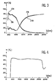
- Figure 3 in the appendix shows the overlay between the experimental spectra in reflection and transmission and recalculated or modeled for one of them.
- the abscissa axis represents the wavelength ⁇ in nm
- the axis of ordered represents the transmission or reflection in percent.
- the curves referenced 5A and 5B represent respectively the spectra of transmission and reflection calculated by the model of Drude and the curves referenced 7A and 7B represent respectively the transmission and reflection obtained according to the invention.
- the tin-doped indium oxide was deposited by magnetron cathode sputtering on glass, from a sintered target whose composition is 10% by weight of tin oxide in In 2 O 3 .
- the optical quality of this oxide deposited in a thin layer depends on the oxygen content in the film as well as its crystalline state.
- FIG. 11 in the appendix illustrates the effect of annealing ITO layer on the optical properties of reflection and transmission of this layer.
- the abscissa axis indicates the wavelength ⁇ in nm
- the references 39A and 39B indicate respectively the transmission and reflection spectra of the ITO without annealed
- references 41A and 41B indicate respectively the transmission and reflection of the ITO with annealing at 200 ° C
- the 43A and 43B indicate respectively the transmission and reflection spectra of ITO with annealing at 300 ° C.
- Heat treatment at 200 ° C is not enough for fill the specifications of the infrared filter.
- the oxide becomes reflective at 80% in the infrared and the cutoff wavelength is at 1.3 ⁇ m.
- the optical properties of this material are then optimized.
- the specifications relating to the performance of the filter are five in number. Table 3 below shows the values to be achieved as well as those obtained with the doped glass filter of the prior art. Desired specifications compared to the performances obtained by the doped glass filter assembly Definition Wanted specifications Doped glass filter Energy Radian RE ⁇ 4.5 mW / m 2 .Lux 2.5 to 4 Visible average transmission T Screw ⁇ 60 61.1 Color temperature T COLOR between 3500 and 4000 K 3583 IRC or R A color rendering index ⁇ 90 96.9 R 9 ⁇ 50 82.9
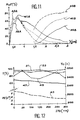
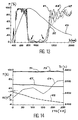
- the inventors studied the performances of stacking according to the thickness of the ITO. For each thickness value, the dielectric part has been recalculated in order to get as close as possible to sought specifications and especially to limit the oscillation effects of the transmission in the part visible spectrum.
- the reference 45 indicates the variation curve of the energy radian RE
- the reference 47 indicates the transmission variation curve T in the visible
- the reference 49 indicates the variation of the temperature of color Tc
- the reference 51 indicates the variation of the color rendering index Ra
- the reference 53 indicates the variation of the color rendering index in the red R 9 .
- the number of layers per group was therefore increased in order to further reduce the level of transmission between 750 and 1200 nm and therefore the radian as shown in Figure 13 in the Annex.
- This figure illustrates the improvement of filtering performance of the architecture with the number of stacks.
- the x-axis represents the wavelength ⁇ in nm and the y-axis transmission in percent.
- Reference 63 indicates the emission spectrum of the source lamp and the arrows indicate the importance of energy radian.
- the performance of the filter especially in the form of the visible transmission window can be improved.
- the reference 65 indicates the variation curve of the radiant energy RE
- the reference 67 indicates the variation curve of the transmission T in the visible
- the reference 69 indicates the variation of the color temperature Tc
- the reference 71 indicates the variation of the color rendering index RA
- the reference 73 indicates the variation of the color rendering index in the red R 9 .
- An ITO thickness of 250 nm makes it possible to reach an energy radian less than or equal to 4.5.
- Trapezoid shaped substrates are made of glass standard. This cutting allows to test in size real a set of 6 pieces assembled around a source lamp, under operational conditions.
- This glass has been characterized in ellipsometry and transmission. Its thickness is 2 mm and the spectrum transmission of a naked sample is proposed on the figure 4 in the appendix. In this figure, T represents the transmission in percent and ⁇ the wavelength in nm.
- optical properties and k have been extracted in order to accurately calculate the total transmission spectrum of the filter on this substrate.
- the ITO layer is deposited on the glass substrate by reactive magnetron sputtering. It is annealed at 300 ° C. under an N 2 atmosphere for 1 hour. The transmission and reflection spectra are measured to verify that the ITO has the right optical characteristics.
- the SiO 2 / TiO 2 stack is then deposited by evaporation as previously described.
- the deposition rate of the layers is controlled by a quartz scale that drives the ion and electron guns.
- the deposition of the 33 dielectric layers lasts about 6 hours.
- the stack obtained is given in Table 4 below: Stacking obtained Layer Material Thickness (nm) 34 SiO 2 64 33 TiO 2 85 32 SiO 2 155 31 TiO 2 89 30 SiO 2 147 29 TiO 2 87 28 SiO 2 144 27 TiO 2 87 26 SiO 2 153 25 TiO 2 85 24 SiO 2 145 23 TiO 2 91 22 SiO 2 149 21 TiO 2 91 20 SiO 2 157 19 TiO 2 94 18 SiO 2 169 17 TiO 2 112 16 SiO 2 189 15 TiO 2 121 14 SiO 2 191 13 TiO 2 125 12 SiO 2 193 11 TiO 2 123 10 SiO 2 192 9 TiO 2 124 8 SiO 2 199 7 TiO 2 124 6 SiO 2 197 5 TiO 2 128 4 SiO 2 190 3 TiO 2 119 2 SiO 2 172 1 ITO 250 substratum Glass
- the transmission spectrum obtained on the stack manufactured is proposed in Figure 15 in the Annex and superimposed on the theoretical spectrum.
- the axis abscissa represents the wavelength in nm and the y-axis the transmission in percent.
- the reference 75 indicates the theoretical spectrum, and the reference 77 the experimental spectrum obtained.
- the shift of the transmission window to the weaker wavelengths comes from some imprecision in the thickness control during the growth. This is confirmed by a mechanical measurement on the edge of the filter which indicates 4.26 ⁇ m at instead of the 4.49 ⁇ m expected.
- Table 5 groups the values of the parameters calculated with this experimental stack. Apart from this visible transmission problem, all these values correspond to the desired specifications. Requested specifications, theoretical and experimental results Theoretical values Experimental values Energy radian RE (mW / m 2 / Lux) 4.45 3.92 Visible average transmission T VIS 65.3% 50.8% Color temperature T COLOR 3514 3490 IRC or R A color rendering index (CIE standards ) 97.3 97.4 R 9 (CIE standards ) 97.0 89.2
- Example 2 Filter of the present invention in which the interference filter is an SiO 2 / Si 3 N 4 filter
- the SiO 2 / Si 3 N 4 filter was deposited by IDECR ("Integrated Distributed Electron Cyclotron Resonance") microwave plasma.
- IDECR Integrated Distributed Electron Cyclotron Resonance
- the interest of such a device is the deposition at low temperature. Indeed, it is possible to deposit a layer of SiO 2 on a polycarbonate substrate having good optical qualities. Moreover, the geometrical configuration of this type of reactor allows the deposition on large surfaces.
- the monolayer nitride and silicon oxide indices were determined. Using their dispersion spectra for the calculation of the transmission spectrum, the following stack of 25 layers on glass (L: SiO 2 , H: Si 3 N 4 ) was carried out: 6 x (0.5L / H / 0.5L) + 6 x (0.65L / 1.3H / 0.65L)
- Figure 17 in the appendix contains the spectra of theoretical and experimental transmission of the stack realized.
- the abscissa axis represents the wavelength ⁇ in nm and the axis of ordered represents the transmission in the visible in percent.
- Reference 79 indicates the theoretical spectrum and reference 81 indicates the experimental spectrum.
- the abscissa axis represents the thickness of ITO in nm
- the left ordinate axis, in its lower part represents the energy radian in mW / m 2 .Lux and in its upper part the transmission in percent
- the ordinate axis on the right represents the color temperature in K.
- the reference 83 indicates the curve of variation of the radiant energy RE
- the reference 85 indicates the transmission variation curve T in the visible
- the reference 87 indicates the variation of the color temperature Tc
- the reference 89 indicates the variation of the color rendering index RA
- the reference 91 indicates the variation of the index color rendering in the red R 9 .
- the inventors have determined an architecture pattern allowing to meet requested specifications in the visible domain.
- they have chosen in particular the pair of high-contrast dielectric materials of index TiO 2 / SiO 2 .
- the second part of this work consisted of define and deposit an infrared reflector material to filter any radiation after 1.5 ⁇ m and not disturbing the optical properties of the filter dielectric. ITO meets these specifications. They determined the deposit parameters and applied a heat treatment after deposition, in order to optimize the material.
Landscapes
- Chemical & Material Sciences (AREA)
- Materials Engineering (AREA)
- Engineering & Computer Science (AREA)
- Chemical Kinetics & Catalysis (AREA)
- General Chemical & Material Sciences (AREA)
- Geochemistry & Mineralogy (AREA)
- Life Sciences & Earth Sciences (AREA)
- Organic Chemistry (AREA)
- Optical Filters (AREA)
- Filtering Materials (AREA)
- Radiation-Therapy Devices (AREA)
- Solid-Sorbent Or Filter-Aiding Compositions (AREA)
- Laminated Bodies (AREA)
- Surface Treatment Of Glass (AREA)
Claims (23)
- Wärmeabsorbierender Filter mit einem Substrat, wenigstens einer Schicht aus einem IR-reflektierenden Material und einem Überzug, der einen Interferenzfilter im sichtbaren Bereich bildet,
dadurch gekennzeichnet, dass der einen Interferenzfilter im sichtbaren Bereich bildende Überzug wenigstens zwei unterschiedliche Stapelgruppen umfasst, wobei eine erste Stapelgruppe eine N-mal wiederholte Abwechslung eines ersten Films und eines zweiten Films aufweist, eine zweite Stapelgruppe eine N-mal wiederholte Abwechslung eines dritten Films und eines vierten Films aufweist, und der erste und/oder der zweite Film sich jeweils vom dritten und/oder vierten Film durch ihre Dicke unterscheiden, der erste und der dritte Film eine Dicke L oder ein Vielfaches von L haben und durch ein erstes Material mit einer Brechzahl n1 gebildet werden, und das zweite und das vierte Material eine Dicke H oder ein Vielfaches von H haben und durch ein zweites Material mit einer Brechzahl n2 gebildet werden, bei dem N eine ganze Zahl ≥3 ist und H und L geometrische Dicken sind, und bei dem N, H, L, n1 und n2 derartig sind, dass der einen Interferenzfilter bildende Überzug ein Transmissionsfenster zwischen 400 und 800 nm aufweist. - Wärmeabsorbierender Filter nach Anspruch 1, bei dem die Schicht aus IRreflektierendem Material wenigstens eine Oberfläche des Substrats bedeckt, und der einen Interferenzfilter im sichtbaren Bereich bildende Überzug die genannte Schicht aus IRreflektierendem Material bedeckt.
- Filter nach Anspruch 1 oder 2, bei dem das IR-reflektierende Material ein transparentes leitfähiges Oxid ist.
- Filter nach Anspruch 1 oder 2, bei dem das IR-reflektierende Material Zinndotiertes Indiumoxid ist.
- Filter nach Anspruch 4, bei dem das Zinn-dotierte Indiumoxid ein Sn/In-Verhältnis aufweist, das von ungefähr 9 bis ungefähr 11 Massenprozent geht.
- Filter nach Anspruch 5, bei dem das erste Material SiO2 ist und das zweite Material TiO2 ist.
- Filter nach Anspruch 6, bei dem der einen Interferenzfilter im sichtbaren Bereich bildende Überzug eine erste Stapelgruppe umfasst, die eine 8-mal wiederholte Abwechslung des Typs 0,5L/H/0,5L aufweist.
- Filter nach Anspruch 7, außerdem eine zweite Stapelgruppe umfassend, die eine 8-mal wiederholte Abwechslung des Typs 0,65L/1,3H/0,65L aufweist.
- Filter nach Anspruch 5, bei dem das erste Material SiO2 ist und das zweite Material Si3N4 ist.
- Filter nach Anspruch 9, bei dem der einen Interferenzfilter im sichtbaren Bereich bildende Überzug eine erste Stapelgruppe mit einer 6-mal wiederholten Abwechslung des Typs 0,5L/H/0,5L aufweist.
- Filter nach Anspruch 10, außerdem eine zweite Stapelgruppe umfassend, die eine 6-mal wiederholte Abwechslung des Typs 0,65L/1,3H/0,65L aufweist.
- Wärmeabsorbierender Filter nach Anspruch 2, bei dem das Substrat ein Glassubstrat ist, die transparente leitfähige Schicht eine Zinn-dotierte Indiumoxidschicht ist, und der einen Interferenzfilter im sichtbaren Bereich bildende Überzug ein Schichtenstapel ist, in dem SiO2-Filme und TiO2-Filme abwechseln, wobei der Schichtenstapel mit einem SiO2-Film, abgeschieden auf der ITO-Schicht, beginnt und mit einem SiO2-Film in Kontakt mit der Atmosphäre endet und dieser Schichtenstapel dabei 17 SiO2-Filme und 16 TiO2-Filme umfasst.
- Wärmeabsorbierender Filter nach Anspruch 1, bei dem das Substrat ein Glas- oder Kunststoffsubstrat ist.
- Wärmeabsorbierender Filter mit einem Glassubstrat, einer ITO-Schicht und einem einen Interferenzfilter im sichtbaren Bereich bildenden Überzug, dadurch gekennzeichnet, dass er zwei unterschiedliche Stapelgruppen von SiO2-Filmen und von TiO2-Filmen umfasst, wobei jede Stapelgruppe eine 8-mal wiederholte Abwechslung von SiO2-Filmen und TiO2-Filmen aufweist und der genannte Filter dabei die folgende Struktur hat:
Schicht Material Dicke (nm) 34 SiO2 64 33 TiO2 85 32 SiO2 155 31 TiO2 89 30 SiO2 147 29 TiO2 87 28 SiO2 144 27 TiO2 87 26 SiO2 153 25 TiO2 85 24 SiO2 145 23 TiO2 91 22 SiO2 149 21 TiO2 91 20 SiO2 157 19 TiO2 94 18 SiO2 169 17 TiO2 112 16 SiO2 189 15 TiO2 121 14 SiO2 191 13 TiO2 125 12 SiO2 193 11 TiO2 123 10 SiO2 192 9 TiO2 124 8 SiO2 199 7 TiO2 124 6 SiO2 197 5 TiO2 128 4 SiO2 190 3 TiO2 119 2 SiO2 172 1 ITO 250 Substrat Glas - Optisches System, ausgewählt aus einer Gruppe, die eine Lampe, eine Bürolampe, ein Beleuchtungssystem mittels optischer Fasern, eine Verglasung, ein optisches Projektionssystem und eine Glüh- bzw. Glasbirne umfasst, dadurch gekennzeichnet, dass sie einen Filter nach einem der vorangehenden Ansprüche 1 bis 14 umfasst.
- Operationsbeleuchtung oder Behandlungslampe, dadurch gekennzeichnet, dass sie einen wärmeabsorbierenden Filter nach einem der vorangehenden Ansprüche 1 bis 14 umfasst.
- Verfahren zur Herstellung des wärmeabsorbierenden Filters, dadurch gekennzeichnet, dass es umfasst:a) Bereitstellen eines Substrats,b) Abscheiden einer Schicht aus einem IR-reflektierenden Material auf wenigstens einer Oberfläche des genannten Substrats,c) Abscheiden - auf der IR-reflektierenden Schicht - eines einen Interferenzfilter im sichtbaren Bereich bildenden Überzugs, wie beschrieben in Anspruch 1.
- Verfahren nach Anspruch 17, bei dem das IR-reflektierende Material Zinndotiertes Indiumoxid ist, abgeschieden auf dem Substrat durch Magnetron-Sputtern.
- Verfahren nach Anspruch 18, bei dem das Magnetron-Sputtern mittels eines Sintertargets erfolgt, dessen Zusammensetzung ungefähr 9 bis 11 Massenprozent Zinnoxid in In2O3 beträgt.
- Verfahren nach Anspruch 18, das außerdem einen Schritt a1) zum Tempern des auf dem Substrat abgeschiedenen IR-reflektierenden Materials umfasst.
- Verfahren nach Anspruch 17, wobei bei dem in dem vorangehenden Anspruch 7 definierten Interferenzfilter der Schritt c) zur Abscheidung des Interferenzfilters ein Schritt zur Abscheidung der realisierten Filme durch eine Vakuumverdampfungs- oder Sputtertechnik ist.
- Verfahren nach Anspruch 17, bei dem der Schritt zur Abscheidung der Filme durch reaktiv unterstützte reaktive Verdampfung realisiert wird.
- Verfahren nach Anspruch 17, wobei bei dem in dem vorangehenden Anspruch 10 definierten Interferenzfilter der Schritt c) zur Abscheidung des Interferenzfilters ein Schritt zur Abscheidung der realisierten Filme durch eine Plasmaabscheidungstechnik ist.
Applications Claiming Priority (3)
| Application Number | Priority Date | Filing Date | Title |
|---|---|---|---|
| FR9914896A FR2801684B1 (fr) | 1999-11-26 | 1999-11-26 | Filtre anticalorique et procede de fabrication de ce filtre |
| FR9914896 | 1999-11-26 | ||
| PCT/FR2000/003280 WO2001038246A2 (fr) | 1999-11-26 | 2000-11-24 | Filtre anticalorique et procede de fabrication de ce filtre |
Publications (2)
| Publication Number | Publication Date |
|---|---|
| EP1232407A2 EP1232407A2 (de) | 2002-08-21 |
| EP1232407B1 true EP1232407B1 (de) | 2003-09-17 |
Family
ID=9552576
Family Applications (1)
| Application Number | Title | Priority Date | Filing Date |
|---|---|---|---|
| EP00988872A Expired - Lifetime EP1232407B1 (de) | 1999-11-26 | 2000-11-24 | Wärmeabsorbierender filter und verfahren zu dessen herstellung |
Country Status (7)
| Country | Link |
|---|---|
| US (1) | US6844976B1 (de) |
| EP (1) | EP1232407B1 (de) |
| JP (1) | JP2003515196A (de) |
| AT (1) | ATE250234T1 (de) |
| DE (1) | DE60005393T2 (de) |
| FR (1) | FR2801684B1 (de) |
| WO (1) | WO2001038246A2 (de) |
Families Citing this family (40)
| Publication number | Priority date | Publication date | Assignee | Title |
|---|---|---|---|---|
| US6919133B2 (en) * | 2002-03-01 | 2005-07-19 | Cardinal Cg Company | Thin film coating having transparent base layer |
| DE10326359B4 (de) * | 2003-06-04 | 2005-10-06 | Deutsches Zentrum für Luft- und Raumfahrt e.V. | Film-Scanner |
| US8524051B2 (en) * | 2004-05-18 | 2013-09-03 | Centre Luxembourg de Recherches pour le Verre et al Ceramique S. A. (C.R.V.C.) | Coated article with oxidation graded layer proximate IR reflecting layer(s) and corresponding method |
| EP1650173A1 (de) * | 2004-10-19 | 2006-04-26 | Applied Films GmbH & Co. KG | Glasbeschichtung |
| DE602005014131D1 (de) | 2004-10-29 | 2009-06-04 | Alcon Inc | Farbkompensierender netzhautsicherheitsfilter |
| US7411643B2 (en) * | 2005-03-03 | 2008-08-12 | Chunghwa Picture Tubes, Ltd. | Liquid crystal display device and inspection method thereof |
| JP5076897B2 (ja) * | 2005-08-16 | 2012-11-21 | 旭硝子株式会社 | 赤外線反射ガラス板および車両窓用合わせガラス |
| WO2007049478A1 (ja) * | 2005-10-26 | 2007-05-03 | Central Glass Company, Limited | 近赤外線反射基板およびその基板を用いた近赤外線反射合わせガラス、近赤外線反射複層ガラス |
| US20070228986A1 (en) * | 2006-03-31 | 2007-10-04 | General Electric Company | Light source incorporating a high temperature ceramic composite for selective emission |
| US7722421B2 (en) * | 2006-03-31 | 2010-05-25 | General Electric Company | High temperature ceramic composite for selective emission |
| US8044567B2 (en) * | 2006-03-31 | 2011-10-25 | General Electric Company | Light source incorporating a high temperature ceramic composite and gas phase for selective emission |
| US7851985B2 (en) * | 2006-03-31 | 2010-12-14 | General Electric Company | Article incorporating a high temperature ceramic composite for selective emission |
| JP2010111516A (ja) * | 2007-01-24 | 2010-05-20 | Toyota Motor Corp | ストレス軽減ガラス |
| US10048415B2 (en) | 2007-08-12 | 2018-08-14 | Toyota Motor Engineering & Manufacturing North America, Inc. | Non-dichroic omnidirectional structural color |
| US10870740B2 (en) | 2007-08-12 | 2020-12-22 | Toyota Jidosha Kabushiki Kaisha | Non-color shifting multilayer structures and protective coatings thereon |
| US10788608B2 (en) | 2007-08-12 | 2020-09-29 | Toyota Jidosha Kabushiki Kaisha | Non-color shifting multilayer structures |
| US9229140B2 (en) * | 2007-08-12 | 2016-01-05 | Toyota Motor Engineering & Manufacturing North America, Inc. | Omnidirectional UV-IR reflector |
| US9063291B2 (en) * | 2007-08-12 | 2015-06-23 | Toyota Motor Engineering & Manufacturing North America, Inc. | Omnidirectional reflector |
| US9739917B2 (en) | 2007-08-12 | 2017-08-22 | Toyota Motor Engineering & Manufacturing North America, Inc. | Red omnidirectional structural color made from metal and dielectric layers |
| US9612369B2 (en) | 2007-08-12 | 2017-04-04 | Toyota Motor Engineering & Manufacturing North America, Inc. | Red omnidirectional structural color made from metal and dielectric layers |
| US10690823B2 (en) | 2007-08-12 | 2020-06-23 | Toyota Motor Corporation | Omnidirectional structural color made from metal and dielectric layers |
| WO2009064753A1 (en) * | 2007-11-12 | 2009-05-22 | Cornell University | Non-imaging, weakly focused fluorescence emission apparatus and methods |
| CN101909509B (zh) * | 2007-11-12 | 2013-03-27 | 康奈尔大学 | 多路径、多放大率、非共焦荧光发射内窥镜装置和方法 |
| JP2011043713A (ja) * | 2009-08-21 | 2011-03-03 | Nikon Corp | 光学装置 |
| TWI447441B (zh) | 2010-11-08 | 2014-08-01 | Ind Tech Res Inst | 紅外光阻隔多層膜結構 |
| CN202177716U (zh) * | 2011-07-22 | 2012-03-28 | 浙江水晶光电科技股份有限公司 | 高像素影像系统用滤光片 |
| AU2012201024B2 (en) * | 2012-02-22 | 2013-12-19 | Industrial Technology Research Institute | Multilayered Infrared Light Reflective Structure |
| US9678260B2 (en) | 2012-08-10 | 2017-06-13 | Toyota Motor Engineering & Manufacturing North America, Inc. | Omnidirectional high chroma red structural color with semiconductor absorber layer |
| US9658375B2 (en) | 2012-08-10 | 2017-05-23 | Toyota Motor Engineering & Manufacturing North America, Inc. | Omnidirectional high chroma red structural color with combination metal absorber and dielectric absorber layers |
| US9664832B2 (en) | 2012-08-10 | 2017-05-30 | Toyota Motor Engineering & Manufacturing North America, Inc. | Omnidirectional high chroma red structural color with combination semiconductor absorber and dielectric absorber layers |
| CN103245992A (zh) * | 2013-04-25 | 2013-08-14 | 兰州空间技术物理研究所 | 1.55~1.75μm透过短波红外滤光片及制备方法 |
| CN103245995B (zh) * | 2013-04-25 | 2015-06-10 | 兰州空间技术物理研究所 | 10.3~11.3μm透过长波红外滤光片及制备方法 |
| US9581741B1 (en) * | 2013-05-31 | 2017-02-28 | Itn Energy Systems, Inc. | Infrared control coating of thin film devices |
| JP6741586B2 (ja) | 2014-04-01 | 2020-08-19 | トヨタ モーター エンジニアリング アンド マニュファクチャリング ノース アメリカ,インコーポレイティド | 色シフトのない多層構造 |
| PL3218317T3 (pl) | 2014-11-13 | 2019-03-29 | Gerresheimer Glas Gmbh | Filtr cząstek urządzenia do wytwarzania szkła, jednostka tłoka, głowica dmuchu, wspornik głowicy dmuchu i urządzenie do wytwarzania szkła, przystosowane lub zawierające filtr |
| US9810824B2 (en) | 2015-01-28 | 2017-11-07 | Toyota Motor Engineering & Manufacturing North America, Inc. | Omnidirectional high chroma red structural colors |
| CN108474870A (zh) | 2016-03-09 | 2018-08-31 | 株式会社Lg化学 | 抗反射膜 |
| CN109656035B (zh) * | 2018-12-17 | 2021-10-08 | 惠科股份有限公司 | 一种显示面板封框胶的检测方法和显示面板、显示装置 |
| US12481028B2 (en) * | 2019-06-05 | 2025-11-25 | Corning Incorporated | Hardened optical windows with anti-reflective, reflective, and absorbing layers for infrared sensing systems |
| CN116325164A (zh) * | 2020-10-13 | 2023-06-23 | 日本板硝子株式会社 | 滤光器、光学装置和光吸收性组合物 |
Family Cites Families (12)
| Publication number | Priority date | Publication date | Assignee | Title |
|---|---|---|---|---|
| DE3201783A1 (de) * | 1982-01-21 | 1983-09-08 | Leybold-Heraeus GmbH, 5000 Köln | Verfahren zum herstellen von in der draufsicht und durchsicht weitgehend farbneutralen, einen hohen infrarotanteil der strahlung reflektierenden scheiben durch katodenzerstaeubung von targets sowie durch das verfahren hergestellte glasscheiben |
| JPS58209549A (ja) * | 1982-06-01 | 1983-12-06 | 株式会社豊田中央研究所 | 熱線しゃへい積層体 |
| JPS5945943A (ja) * | 1982-09-07 | 1984-03-15 | Nippon Soken Inc | 熱線遮断ガラス |
| CA2017471C (en) * | 1989-07-19 | 2000-10-24 | Matthew Eric Krisl | Optical interference coatings and lamps using same |
| US5296961A (en) * | 1991-04-23 | 1994-03-22 | Coherent, Inc. | Dichroic optical filter |
| US5179468A (en) * | 1991-11-05 | 1993-01-12 | Gte Products Corporation | Interleaving of similar thin-film stacks for producing optical interference coatings |
| US5667880A (en) * | 1992-07-20 | 1997-09-16 | Fuji Photo Optical Co., Ltd. | Electroconductive antireflection film |
| US5360659A (en) * | 1993-05-24 | 1994-11-01 | The Dow Chemical Company | Two component infrared reflecting film |
| FR2734811B1 (fr) * | 1995-06-01 | 1997-07-04 | Saint Gobain Vitrage | Substrats transparents revetus d'un empilement de couches minces a proprietes de reflexion dans l'infrarouge et/ou dans le domaine du rayonnement solaire |
| US5750265A (en) * | 1996-01-11 | 1998-05-12 | Libbey-Owens-Ford Co. | Coated glass article having a pyrolytic solar control coating |
| WO1997048115A1 (en) * | 1996-06-12 | 1997-12-18 | The Trustees Of Princeton University | Plasma treatment of conductive layers |
| GB2324098A (en) * | 1997-04-08 | 1998-10-14 | Pilkington Plc | Solar control coated glass |
-
1999
- 1999-11-26 FR FR9914896A patent/FR2801684B1/fr not_active Expired - Fee Related
-
2000
- 2000-11-24 DE DE60005393T patent/DE60005393T2/de not_active Expired - Fee Related
- 2000-11-24 WO PCT/FR2000/003280 patent/WO2001038246A2/fr not_active Ceased
- 2000-11-24 AT AT00988872T patent/ATE250234T1/de not_active IP Right Cessation
- 2000-11-24 JP JP2001539808A patent/JP2003515196A/ja not_active Withdrawn
- 2000-11-24 US US10/130,277 patent/US6844976B1/en not_active Expired - Fee Related
- 2000-11-24 EP EP00988872A patent/EP1232407B1/de not_active Expired - Lifetime
Also Published As
| Publication number | Publication date |
|---|---|
| US6844976B1 (en) | 2005-01-18 |
| FR2801684B1 (fr) | 2002-04-26 |
| DE60005393D1 (de) | 2003-10-23 |
| WO2001038246A2 (fr) | 2001-05-31 |
| FR2801684A1 (fr) | 2001-06-01 |
| EP1232407A2 (de) | 2002-08-21 |
| WO2001038246A3 (fr) | 2002-01-10 |
| JP2003515196A (ja) | 2003-04-22 |
| DE60005393T2 (de) | 2004-07-15 |
| ATE250234T1 (de) | 2003-10-15 |
Similar Documents
| Publication | Publication Date | Title |
|---|---|---|
| EP1232407B1 (de) | Wärmeabsorbierender filter und verfahren zu dessen herstellung | |
| EP2956423B1 (de) | Ionenstrahlbehandlungsverfahren zur herstellung von dauerhaften glasmaterialien mit reflexionsschutz | |
| EP1135335B1 (de) | Dünnfilm aus hafniumoxid und verfahren zum aufbringen | |
| WO2005000758A2 (fr) | Substrat revetu d’une couche dielectrique et procede et installation pour sa fabrication | |
| FR2699164A1 (fr) | Procédé de traitement de couches minces à base d'oxyde ou de nitrure métallique. | |
| CN111679347A (zh) | 一种高损伤阈值激光薄膜工艺技术方法 | |
| EP1529124B1 (de) | Verfahren zur herstellung einer dünnen schicht von stabilisiertem fluorhaltigen silika, so beschichtetes substrat und so erhaltene ophthalmische linse | |
| EP0031278A1 (de) | Interferenzfilter zum Schutz gegen Infrarotstrahlung und Verwendung | |
| FR2820512A1 (fr) | Film fonctionnel aux proprietes optiques et electriques ameliorees | |
| EP0742453A1 (de) | Breitbandspiegel hohen Reflektionsgrads und Verfahren zur Herstellung eines solchen Spiegels | |
| WO2015181500A1 (fr) | Materiau comprenant une couche fonctionnelle a base d'argent cristallisee sur une couche d'oxyde de nickel | |
| WO2013024226A1 (fr) | Vitrage antireflet muni d'un revetement poreux | |
| JP5665751B2 (ja) | 酸化ハフニウム−コーティング | |
| EP0881508A1 (de) | UV Tiefpassfilter | |
| EP3386929A1 (de) | Verfahren und anlage zum erhalt einer farbigen verglasung | |
| Vinokurova et al. | Metallised holographic diffraction gratings with the enhanced radiation resistance for laser pulse compression systems | |
| FR3111842A1 (fr) | Procede d’elaboration et de controle de la qualite d’un empilement oxyde/metal/oxyde | |
| Riera | Selectively absorbing plasmonic metal-island films | |
| EP0143714B1 (de) | Lumineszenter Schirm und Verfahren zur Herstellung desselben | |
| FR2661253A1 (fr) | Element d'optique comportant au moins un empilement de couches dielectriques utilisees pour la reflexion et/ou la transmission de certaines longueurs d'onde, procede pour sa realisation et multiplexeur-demultiplexeur le comportant. | |
| WO2025141034A1 (fr) | Matériau comprenant un revêtement fonctionnel à deux couches à deux couches a base d'argent et un element en couches absorbant | |
| JP2003172805A (ja) | 反射防止膜付き屈折率分布レンズ | |
| EP4543818A1 (de) | Transparenter glasartikel für ein kühlfach und mehrfachverglasungseinheit mit dem artikel | |
| Vandendriessche | No One-Size-Fits-All Approach to Selecting Optical Coatings | |
| WO2025141032A1 (fr) | Matériau comprenant un revêtement fonctionnel à deux couches à deux couches a base d'argent et un element en couches absorbant |
Legal Events
| Date | Code | Title | Description |
|---|---|---|---|
| PUAI | Public reference made under article 153(3) epc to a published international application that has entered the european phase |
Free format text: ORIGINAL CODE: 0009012 |
|
| 17P | Request for examination filed |
Effective date: 20020522 |
|
| AK | Designated contracting states |
Kind code of ref document: A2 Designated state(s): AT BE CH CY DE DK ES FI FR GB GR IE IT LI LU MC NL PT SE TR |
|
| AX | Request for extension of the european patent |
Free format text: AL;LT;LV;MK;RO;SI |
|
| GRAH | Despatch of communication of intention to grant a patent |
Free format text: ORIGINAL CODE: EPIDOS IGRA |
|
| GRAS | Grant fee paid |
Free format text: ORIGINAL CODE: EPIDOSNIGR3 |
|
| GRAA | (expected) grant |
Free format text: ORIGINAL CODE: 0009210 |
|
| AK | Designated contracting states |
Kind code of ref document: B1 Designated state(s): AT BE CH CY DE DK ES FI FR GB GR IE IT LI LU MC NL PT SE TR |
|
| PG25 | Lapsed in a contracting state [announced via postgrant information from national office to epo] |
Ref country code: TR Free format text: LAPSE BECAUSE OF FAILURE TO SUBMIT A TRANSLATION OF THE DESCRIPTION OR TO PAY THE FEE WITHIN THE PRESCRIBED TIME-LIMIT Effective date: 20030917 Ref country code: IT Free format text: LAPSE BECAUSE OF FAILURE TO SUBMIT A TRANSLATION OF THE DESCRIPTION OR TO PAY THE FEE WITHIN THE PRE;WARNING: LAPSES OF ITALIAN PATENTS WITH EFFECTIVE DATE BEFORE 2007 MAY HAVE OCCURRED AT ANY TIME BEFORE 2007. THE CORRECT EFFECTIVE DATE MAY BE DIFFERENT FROM THE ONE RECORDED.SCRIBED TIME-LIMIT Effective date: 20030917 Ref country code: IE Free format text: LAPSE BECAUSE OF FAILURE TO SUBMIT A TRANSLATION OF THE DESCRIPTION OR TO PAY THE FEE WITHIN THE PRESCRIBED TIME-LIMIT Effective date: 20030917 Ref country code: FI Free format text: LAPSE BECAUSE OF FAILURE TO SUBMIT A TRANSLATION OF THE DESCRIPTION OR TO PAY THE FEE WITHIN THE PRESCRIBED TIME-LIMIT Effective date: 20030917 Ref country code: AT Free format text: LAPSE BECAUSE OF FAILURE TO SUBMIT A TRANSLATION OF THE DESCRIPTION OR TO PAY THE FEE WITHIN THE PRESCRIBED TIME-LIMIT Effective date: 20030917 |
|
| REG | Reference to a national code |
Ref country code: GB Ref legal event code: FG4D Free format text: NOT ENGLISH |
|
| REG | Reference to a national code |
Ref country code: CH Ref legal event code: EP |
|
| REF | Corresponds to: |
Ref document number: 60005393 Country of ref document: DE Date of ref document: 20031023 Kind code of ref document: P |
|
| REG | Reference to a national code |
Ref country code: IE Ref legal event code: FG4D Free format text: FRENCH |
|
| PG25 | Lapsed in a contracting state [announced via postgrant information from national office to epo] |
Ref country code: LU Free format text: LAPSE BECAUSE OF NON-PAYMENT OF DUE FEES Effective date: 20031124 Ref country code: CY Free format text: LAPSE BECAUSE OF FAILURE TO SUBMIT A TRANSLATION OF THE DESCRIPTION OR TO PAY THE FEE WITHIN THE PRESCRIBED TIME-LIMIT Effective date: 20031124 |
|
| PG25 | Lapsed in a contracting state [announced via postgrant information from national office to epo] |
Ref country code: MC Free format text: LAPSE BECAUSE OF NON-PAYMENT OF DUE FEES Effective date: 20031130 Ref country code: BE Free format text: LAPSE BECAUSE OF NON-PAYMENT OF DUE FEES Effective date: 20031130 |
|
| GBT | Gb: translation of ep patent filed (gb section 77(6)(a)/1977) | ||
| PG25 | Lapsed in a contracting state [announced via postgrant information from national office to epo] |
Ref country code: SE Free format text: LAPSE BECAUSE OF FAILURE TO SUBMIT A TRANSLATION OF THE DESCRIPTION OR TO PAY THE FEE WITHIN THE PRESCRIBED TIME-LIMIT Effective date: 20031217 Ref country code: GR Free format text: LAPSE BECAUSE OF FAILURE TO SUBMIT A TRANSLATION OF THE DESCRIPTION OR TO PAY THE FEE WITHIN THE PRESCRIBED TIME-LIMIT Effective date: 20031217 Ref country code: DK Free format text: LAPSE BECAUSE OF FAILURE TO SUBMIT A TRANSLATION OF THE DESCRIPTION OR TO PAY THE FEE WITHIN THE PRESCRIBED TIME-LIMIT Effective date: 20031217 |
|
| PG25 | Lapsed in a contracting state [announced via postgrant information from national office to epo] |
Ref country code: ES Free format text: LAPSE BECAUSE OF FAILURE TO SUBMIT A TRANSLATION OF THE DESCRIPTION OR TO PAY THE FEE WITHIN THE PRESCRIBED TIME-LIMIT Effective date: 20031228 |
|
| PG25 | Lapsed in a contracting state [announced via postgrant information from national office to epo] |
Ref country code: PT Free format text: LAPSE BECAUSE OF FAILURE TO SUBMIT A TRANSLATION OF THE DESCRIPTION OR TO PAY THE FEE WITHIN THE PRESCRIBED TIME-LIMIT Effective date: 20031229 |
|
| LTIE | Lt: invalidation of european patent or patent extension |
Effective date: 20030917 |
|
| REG | Reference to a national code |
Ref country code: IE Ref legal event code: FD4D |
|
| BERE | Be: lapsed |
Owner name: *ALM Effective date: 20031130 Owner name: COMMISSARIAT A L'*ENERGIE ATOMIQUE Effective date: 20031130 |
|
| PLBE | No opposition filed within time limit |
Free format text: ORIGINAL CODE: 0009261 |
|
| STAA | Information on the status of an ep patent application or granted ep patent |
Free format text: STATUS: NO OPPOSITION FILED WITHIN TIME LIMIT |
|
| PG25 | Lapsed in a contracting state [announced via postgrant information from national office to epo] |
Ref country code: FR Free format text: LAPSE BECAUSE OF NON-PAYMENT OF DUE FEES Effective date: 20040730 |
|
| 26N | No opposition filed |
Effective date: 20040618 |
|
| REG | Reference to a national code |
Ref country code: FR Ref legal event code: ST |
|
| PGFP | Annual fee paid to national office [announced via postgrant information from national office to epo] |
Ref country code: NL Payment date: 20041103 Year of fee payment: 5 |
|
| PGFP | Annual fee paid to national office [announced via postgrant information from national office to epo] |
Ref country code: GB Payment date: 20041124 Year of fee payment: 5 |
|
| PGFP | Annual fee paid to national office [announced via postgrant information from national office to epo] |
Ref country code: CH Payment date: 20041129 Year of fee payment: 5 |
|
| PGFP | Annual fee paid to national office [announced via postgrant information from national office to epo] |
Ref country code: DE Payment date: 20041201 Year of fee payment: 5 |
|
| PG25 | Lapsed in a contracting state [announced via postgrant information from national office to epo] |
Ref country code: GB Free format text: LAPSE BECAUSE OF NON-PAYMENT OF DUE FEES Effective date: 20051124 |
|
| PG25 | Lapsed in a contracting state [announced via postgrant information from national office to epo] |
Ref country code: LI Free format text: LAPSE BECAUSE OF NON-PAYMENT OF DUE FEES Effective date: 20051130 Ref country code: CH Free format text: LAPSE BECAUSE OF NON-PAYMENT OF DUE FEES Effective date: 20051130 |
|
| PG25 | Lapsed in a contracting state [announced via postgrant information from national office to epo] |
Ref country code: NL Free format text: LAPSE BECAUSE OF NON-PAYMENT OF DUE FEES Effective date: 20060601 Ref country code: DE Free format text: LAPSE BECAUSE OF NON-PAYMENT OF DUE FEES Effective date: 20060601 |
|
| REG | Reference to a national code |
Ref country code: CH Ref legal event code: PL |
|
| GBPC | Gb: european patent ceased through non-payment of renewal fee |
Effective date: 20051124 |
|
| NLV4 | Nl: lapsed or anulled due to non-payment of the annual fee |
Effective date: 20060601 |