EP1233341B1 - Analyseur logique intégré - Google Patents
Analyseur logique intégré Download PDFInfo
- Publication number
- EP1233341B1 EP1233341B1 EP02009367A EP02009367A EP1233341B1 EP 1233341 B1 EP1233341 B1 EP 1233341B1 EP 02009367 A EP02009367 A EP 02009367A EP 02009367 A EP02009367 A EP 02009367A EP 1233341 B1 EP1233341 B1 EP 1233341B1
- Authority
- EP
- European Patent Office
- Prior art keywords
- pld
- logic analyzer
- logic
- design
- jtag port
- Prior art date
- Legal status (The legal status is an assumption and is not a legal conclusion. Google has not performed a legal analysis and makes no representation as to the accuracy of the status listed.)
- Expired - Lifetime
Links
Images


Classifications
-
- G—PHYSICS
- G06—COMPUTING OR CALCULATING; COUNTING
- G06F—ELECTRIC DIGITAL DATA PROCESSING
- G06F11/00—Error detection; Error correction; Monitoring
- G06F11/36—Prevention of errors by analysis, debugging or testing of software
- G06F11/362—Debugging of software
- G06F11/3648—Debugging of software using additional hardware
-
- G—PHYSICS
- G01—MEASURING; TESTING
- G01R—MEASURING ELECTRIC VARIABLES; MEASURING MAGNETIC VARIABLES
- G01R31/00—Arrangements for testing electric properties; Arrangements for locating electric faults; Arrangements for electrical testing characterised by what is being tested not provided for elsewhere
- G01R31/28—Testing of electronic circuits, e.g. by signal tracer
- G01R31/317—Testing of digital circuits
- G01R31/3177—Testing of logic operation, e.g. by logic analysers
-
- G—PHYSICS
- G06—COMPUTING OR CALCULATING; COUNTING
- G06F—ELECTRIC DIGITAL DATA PROCESSING
- G06F11/00—Error detection; Error correction; Monitoring
- G06F11/22—Detection or location of defective computer hardware by testing during standby operation or during idle time, e.g. start-up testing
- G06F11/26—Functional testing
- G06F11/27—Built-in tests
Definitions
- Programmable logic devices refer to any integrated circuit that may be programmed to perform a desired function and include programmable logic arrays (PLAs), programmable array logic (PAL), field programmable gate arrays (FPGA), complex programmable logic devices (CPLDs), and a wide variety of other logic and memory devices that may be programmed. Often, such PLDs are designed and programmed by a design engineer using an electronic design automation tool that takes the form of a software package.
- PLDs programmable logic arrays
- PAL programmable array logic
- FPGA field programmable gate arrays
- CPLDs complex programmable logic devices
- creating an electronic design for a PLD is an iterative process that requires creative debugging by an engineer who may wish to view almost any internal signal, and who may change his mind fairly frequently in the course of debugging a PLD within a system.
- Known external and internal logic analyzers do not provide this flexibility.
- an engineer may employ a conventional logic analyzer to study an internal signal of a PLD. This may be accomplished by, for example, an engineer modifying his design so that a normally internal signal is routed temporarily to an output pin of the PLD. The design is then recompiled. The engineer then attaches a probe to this output pin in order to monitor the "internal" signal. Unfortunately, the engineer must recompile his design and reprogram the PLD in order to view this internal signal. Also, when debugging is complete, the engineer must again rewrite the design to remove the internal signal from the output pin, recompile the design and finally reprogram the PLD again. This can be a tedious process.
- a design engineer designs a PLD and programs such a device using an electronic design automation tool.
- the design engineer may perform numerous design-program-debug iterations before the design is complete and the PLD ready for mass manufacturing.
- the design engineer often uses a simulation and/or a timing analysis to assist in debugging the electronic design of the PLD. It is also conceivable that a design engineer would use an embedded logic analyzer (such as disclosed in U.S. patent application No. 08/958,435) to troubleshoot the design.
- a product engineer designs a manufacturing flow for the mass production of an electronic circuit board or other electronic device that incorporates one or more PLDs.
- the manufacturing phase it will be necessary to test the board itself and may also be necessary to retest the PLD.
- any number and type of hardware components and any number of PLDs are soldered to a board.
- a PLD is most often programmed (or configured) using a JTAG port located on the PLD. It is also possible that a particular PLD be programmed by itself before placement on a board using a special socket and a programming unit.
- DE 4042262 discloses a method of analyzing digital circuit functions using scanned values in which digital circuit functions are analyzed by writing values from several data highways into a memory at defined times and displaying them on a screen. As many results as required can be written into the memory with pretrace or pretrace and centre trace under control by a trigger unit. Any length of pretrace and/or centre trace can be used. The results can be passed to the memory via a digital delay circuit.
- a JTAG port is used either to program a PLD or to assist with testing a circuit board on which PLDs are located.
- a JTAG port has traditionally been unused during the design and debugging of a particular PLD.
- a JTAG port on a PLD is under utilized and may be used during debugging of a PLD as a means of communicating with and controlling an embedded logic analyzer of the present invention.
- the standard JTAG port is used to facilitate debugging of a programmable logic device that includes an embedded logic analyzer. Use of a JTAG port avoids adding dedicated debugging control pins.
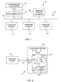
- Programming unit 14 may be any suitable hardware programming unit that accepts program instructions from computer network 12 in order to program PLD 16.
- programming unit 14 may include an add-on logic programmer card for a computer, and a master programming unit, such as are available from Altera Corporation of San Jose, California.
- PLD 16 may be present in a system or in a programming station. In operation, any number of engineers use computer network 12 in order to develop programming instructions using an electronic design automation software tool. Once a design has been developed and entered by the engineers, the design is compiled and verified before being downloaded to the programming unit. The programming unit 14 is then able to use the downloaded design in order to program PLD 16.
- a project includes a project file, design files, assignment files, and simulation files, together with hierarchy information, system settings, and output files, which includes programming files and report files.
- a project database may also exist, which contains intermediate data structures and version information.
- a block is simulated functionally at the source level using a behavioral simulator and vectors generated by using a VHDL or Verilog test bench, for example.
- the simulation results can then be displayed or otherwise presented/recorded as waveforms, text or annotated onto the source files.
- the designer may also return to step 58 to implement a block again. Also, at this point a block may be compiled or a timing analysis performed.
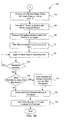
- step 115 the user specifies the number of data samples to be captured prior to the breakpoint.
- the user may specify any number of samples to be captured prior to the breakpoint occurring, thus allowing later analysis of these prior signals to help determine the cause of a failure, error or other condition.
- implementation of the embedded logic analyzer allows samples to be stored continuously which provides a user with any number of samples needed prior to the breakpoint.
- a user may specify the number of samples needed after the breakpoint. Because the total number of samples to be captured has been specified in step 110, it is straightforward to calculate prior samples needed based upon later samples needed, and vice-versa. The user may also specify samples needed prior to the breakpoint and samples needed after the breakpoint; total samples to be captured can then be calculated automatically.
- the cable may attach directly to these pins, or, the signals from these pins may be routed to an easily accessible location or port on the board to which the debugging cable may easily attach.
- the cable will be used to transmit instructions from the computer to the embedded logic analyzer, and also to upload captured information from the logic analyzer to the computer.
- FIG. 5 shows a PLD containing both a user design and an embedded logic analyzer within an electronic system.
- a cable 28 is shown connecting the electronic system to an external computer.
- the stored data is dumped from the sample memory of the logic analyzer to the user's computer in step 132.
- the logic analyzer uploads this stored information over the interface cable to the user's computer.
- the user is able to graphically view these signals received from the logic analyzer.
- the signals are presented in a waveform view annotated with the names of the signals.
- this step makes appropriate connections from the logic analyzer to an interface to the user's computer.
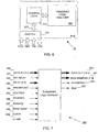
- this interface includes test data registers 274 linked to JTAG port 272. Accordingly, input and output connections to and from the logic analyzer that provide an interface to the user computer are connected to the appropriate test register. For example, as shown in FIGS. 7 and 8, input signals (from the user computer to the logic analyzer) Trigger Signals, Trigger Register, Set Delay, Delay[6:0], NextReq, StopReq, RunReq, and Clear are connected to appropriate test registers.
- Test registers are preferably constructed from programmable logic, and will be familiar to those of skill in the art.
- a JTAG port is used either to program a PLD or to assist with testing a circuit board on which PLDs are located.
- a JTAG port has traditionally been unused during the design and debugging of a particular PLD.
- a JTAG port on a PLD is under utilized and may be used during debugging of a PLD as a means of communicating with and controlling an embedded logic analyzer of the present invention.
- a standard JTAG port is used to facilitate debugging of a programmable logic device that includes an embedded logic analyzer. Two particular embodiments for implementing control logic 274 to facilitate control of an embedded logic analyzer by a JTAG port are described below in FIGS. 11-13 and 14-17, respectively.
- a preferred embodiment of the invention uses JTAG port 272 along with control logic 274 and signals 275 for controlling logic analyzer 260. It is realized that use of a JTAG port for control of a logic analyzer would be advantageous in that a JTAG port is often already present on a PLD. Furthermore, use of a JTAG port would obviate the need to add extra, dedicated debugging control pins. Furthermore, many manufacturers of PLDs already have facilities for connecting and communicating through a JTAG port of a PLD. For example, Altera Corporation of San Jose, California uses an internal product known as "Byte Blaster" to program a PLD through a JTAG port. For these reasons and others, it is realized that use of a JTAG port to control an embedded logic analyzer would be advantageous. Nevertheless, how to implement such control using a JTAG port is not intuitively obvious for a variety of reasons.
- FIG. 11 illustrates a first embodiment by which JTAG port 272 controls embedded logic analyzer 260 of PLD 16 using groups of unbonded I/O cells 504 and 506.
- Logic analyzer 260 is embedded in core 502 of PLD 16 and has a system clock 288.
- Cells 504 deliver signals 514 to the logic analyzer, and cells 506 receive signals 516 from the logic analyzer.
- Signals 275 represent signals from JTAG port 272 to and from I/O cells 504 and 506.
- the netlist of the PLD is augmented to route each input to and each output from logic analyzer 260 to an unbonded or otherwise unused I/O cell 504 or 506, respectively.
- a special "debug RAM bit" is set for each I/O cell that is used to supply a control signal to the logic analyzer; this bit allows a control signal to be driven using the JTAG port even though the device is not placed into INTEST mode.
- the known JTAG Sample/Preload instruction is scanned in, the control information is scanned in, and then the Update/Data Recovery state of JTAG port 272 is entered. Further details are provided below. To better illustrate the advantages of this embodiment, the known JTAG INTEST mode will be briefly described.
- FIG. 12 illustrates a prior art JTAG-enabled I/O cell 600 that provides a useful background for discussion of this embodiment.
- Cell 600 connects to an external PLD pin 602. Through pin 602, input signal 604 is provided to core 502 of PLD 16. Similarly, signals output 606 and output enable 608 originate within core 502 and are used to produce an output signal at pin 602.
- Multiplexers 610, 612 and 614 select data to be loaded into capture registers 620, 622 and 624, respectively.
- the capture registers are used to scan in data initially from JTAG port 272 through the I/O cells of the device.
- Update registers 630, 632 and 634 receive data from the capture registers and are used to perform a parallel load to the core of the device.
- Multiplexers 640, 642 and 644 select data from either pin 602 input, output enable 608, and output 606, respectively, or from one of the update registers to produce an appropriate signal.
- Multiplexer 640 produces input signal 604
- multiplexer 642 produces a tri-state signal for driver 650
- multiplexer 644 provides a data signal for driver 650 which produces an output at pin 602 when enabled.
- Serial data in 672 is a signal received from the previous I/O cell (or from the TDI signal of JTAG port 272 if this is the first cell), and serial data out 674 is connected to the serial data in signal of the next I/O cell (or to signal TDO of JTAG port 272 if this is the last I/O cell).
- Control signals Shift 680, Clock 682, Update 684 and Mode 686 are received for each cell from JTAG port 272 via control lines 275.
- Shift 680 operates to shift the serial data in signal 672 through cell 600.
- mode 686 places the device in INTEST or EXTEST mode
- signals output 606, output enable 608 and input 604 are effectively cut-off from pin 602, and thus, core 502 of the device is isolated from the outside world.
- it would be undesirable to place the device completely into INTEST mode if it is desired to test the device in a real-world environment. For example, if mode 686 places the device into INTEST mode, all pins of the device would be isolated from its core and normal operation of the device would be prevented.
- FIG. 13 illustrates an unbonded I/O cell 504 according to this first embodiment of JTAG control. Additionally included in cell 504 is gate 702 and debug RAM bit 704.
- mode 686 places PLD 16 into its normal mode of operation so that logic analyzer 260 can capture real-world data. In this mode, pins of the PLD are not isolated from core 502.
- JTAG port 272 For unbonded I/O cell 504, however, it is still desirable to be able to use JTAG port 272 to provide a control signal to embedded logic analyzer 260.
- gate 702 and debug RAM bit 704 are provided. Bit 704 is always set; therefore, the output of gate 702 is a logic "1" which directs multiplexer 640 to always produce its output data from update register 630.
- FIG. 14 illustrates a second embodiment by which JTAG port 272 controls embedded logic analyzer 260 using a test data register 802.
- a user implemented test data register 802 is used to provide control signals to, and to receive data and status form, logic analyzer 260.
- This embodiment is particularly useful if no unbonded I/O cells are available. It relies upon extra user-supplied logic in test data register 802 instead of using unbonded I/O cells.
- this embodiment provides an extra signal Runtest(user) that allows logic analyzer 260 to know when the JTAG state machine has entered the Runtest state.
- Register 802 includes any number of stimulus cells 804 used to control logic analyzer 260 and any number of sense cells 805 used for retrieving data and status from the logic analyzer.
- Control signals 806 include signal TDI(user) which is presented to the first stimulus cell and then shifted through all of the cells. Also included are the control signals Shift(user), Clock(user), Update(user), and Runtest(user); these signals are presented globally to each cell 804 or 805. Signal TDO(user) 807 is received from the final sense cell 805 and presented to JTAG port 272 to become signal TDO.
- signal Load(user) is a one; data and/or status arrive via multiplexer 830 and are captured by register 832. Once any number of bits are captured by cells 805 after a parallel load, the captured bits are shifted out using the serial shift mode through JTAG port 272 to computer system 18 for analysis. In this fashion, sense cells 805 are used to retrieve data and/or status from logic analyzer 260 and to present the information to a user for analysis.
- FIGS. 17A, 17B illustrate an alternative embodiment in which any number of logic analyzers embedded within a device are controlled using a JTAG port.
- PLDs As PLDs become larger and larger, it is possible that each megafunction within the device may contain its own embedded logic analyzer. It would be desirable to be able to control any number of embedded logic analyzers using a JTAG port using any of the embodiments discussed herein.
- the second embodiment discussed above in FIGS. 14-16 works well.
- control of one of two embedded logic analyzers may be achieved using a Select signal generated from JTAG port 272.
- private user instructions may be loaded into the JTAG port.
- a UserA instruction and a UserB instruction may be provided. Control information destined for a first logic analyzer is loaded into the UserA instruction; control information destined for a second logic analyzer is loaded into the UserB instruction.
- signal Select goes high, when UserB is loaded, Select goes low.
- Signal Select is then combined with and qualifies the control signals from the JTAG port to be directed to either a first or a second test data register that control respectively, the first or the second embedded logic analyzer.
- a single signal for example, Select
- the second logic analyzer is selected when Select is a logic "0". For more than two logic analyzers to be controlled, it is useful to use an embodiment such as will now be described.
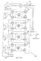
- FIG. 17A illustrates an embodiment in which logic analyzers 260a, 260b, 260c and 260d present within a single PLD are controlled via a JTAG port of the PLD.
- FIG. 17A provides a simplistic example of control of only four logic analyzers having minimal inputs and outputs, those of skill in the art upon a reading of this disclosure will appreciate how to implement control of any number of logic analyzers, and of logic analyzers having more complex inputs and outputs.
- Each logic analyzer 260a-260d is controlled by a respective test data register 860-866.
- logic analyzer 260a is controlled by test data register 860.
- Elements 860a and 860b of register 860 provide control inputs to logic analyzer 260a, and elements 860c and 860d of register 860 receive output data from logic analyzer to 260a.
- the other logic analyzers are controlled in a similar manner.
- two private user instructions within the JTAG port are used to control any number of logic analyzers.
- the UserA instruction contains an address, suitable for selecting which logic analyzer to control and to receive data from at a particular point in time.
- the second private instruction called UserB provides the actual control information and receives data from the logic analyzer that is selected using the UserA instruction.
- the Select signal is also used in this embodiment, and is active depending upon whether information in the UserA or the UserB instruction is being accessed.
- a second private UserB instruction is used to provide the actual control information for the logic analyzer selected by the UserA instruction. Similar to the second embodiment discussed above, signal TDI(UserB) 876 is provided in a serial fashion to each of the test registers 860-866 that control respectively logic analyzers 260a-260d. Serial information received on signal 876 is shifted through the appropriate test data register and eventually is shifted out through multiplexer 874 to become signal TDO(UserB) 890 which is returned to the JTAG port.
- control information would be shifted in via signal 876 to element 866a, shifted then to element 866b, then shifted to element 866c and finally shifted to element 866d.
- output data received from logic analyzer 260d is retrieved using a parallel load into elements 866c and 866d and then shifted out to multiplexer 874.
- control signals such as Shift(user), Clock(user), Update(user), and Runtest(user). These control signals are routed to the selected logic analyzer using decoder 872 and AND gates 882-888.
- signals Clock(UserB) 880 and Clock(UserA) may be generated from signal Clock(user) using AND gates and the signal Select.
- Select When Select is active, Clock(UserA) is clocking and Clock(UserB) is not; an inactive Select produces the opposite. In this fashion, when information from private instruction UserA is being supplied, Select is active and enables the appropriate control signals.
- input control signals such as Clock(user), Shift(user), etc.
- JTAG port would connect directly to the elements of the single test data register.
- Data from the UserB instruction would be shifted into this test data register to provide control for one of the logic analyzers.
- Each input element of the test data register would be routed to each logic analyzer and be qualified by an AND gate, or similar selection circuitry. For example, if three bits of control information are to be supplied from the single test data register to four different logic analyzers, there would be four AND gates for each bit of control information (each associated with a logic analyzer) for a total of twelve AND gates (or similar selection logic).
- multiplexers may be employed to select from which logic analyzers an output signal will be accepted for input to the single test data register.
- a single multiplexer (or similar selection logic) would be used for each element of the test data register that receives output data from the logic analyzer. Routed to this multiplexer are the corresponding data signals from each of the logic analyzers. For example, the least significant data bit from each of the logic analyzers is routed to a single multiplexer that provides output to a single element of the test data register.
- the multiplexer is controlled via bits from the UserA test data register in a similar fashion as shown in FIG. 17A. A multiplexer would be supplied for each output element of the test data register, and each controlled by the same selection logic.
- FIG. 18 illustrates a computer system 900.
- Computer system 900 includes any number of processors 902 (also referred to as central processing units, or CPUs) that are coupled to storage devices including primary storage 906 (such as random access memory, or RAM) and primary storage 904 (such as a read only memory, or ROM).
- primary storage 904 acts to transfer data and instructions uni-directionally to the CPU and primary storage 906 is used typically to transfer data and instructions in a bi-directional manner. Both of these primary storage devices may include any suitable of the computer-readable media described below.
- a mass storage device 908 is also coupled bi-directionally to CPU 902 and provides additional data storage capacity and may also include any of the computer-readable media described below.
- Mass storage device 908 may be used to store programs, data and the like and is typically a secondary storage medium (such as a hard disk) that is slower than primary storage. It will be appreciated that the information retained within mass storage device 908, may, in appropriate cases, be incorporated in standard fashion as part of primary storage 906 as virtual memory.
- a specific mass storage device such as a CD-ROM 914 passes data uni-directionally to the CPU.
Landscapes
- Engineering & Computer Science (AREA)
- General Engineering & Computer Science (AREA)
- Theoretical Computer Science (AREA)
- Computer Hardware Design (AREA)
- Physics & Mathematics (AREA)
- General Physics & Mathematics (AREA)
- Quality & Reliability (AREA)
- Test And Diagnosis Of Digital Computers (AREA)
- Tests Of Electronic Circuits (AREA)
Claims (11)
- Dispositif logique programmable, PLD, (16) comprenant:un circuit de PLD représentant une itération d'une structure électronique dans un processus de conception pour créer un PLD final ;un circuit d'analyseur logique (260) intégré à l'intérieur du circuit de PLD de façon qu'une partie du circuit de PLD soit connectée au circuit d'analyseur logique (260) ;caractérisé par :un port JTAG (272) agencé pour recevoir des ordres d'analyseur logique provenant de l'extérieur du PLD ; etun moyen pour commander (274) le circuit d'analyseur logique (260) en utilisant le port JTAG (272) du PLD (16), grâce à quoi le circuit d'analyseur logique (260) reçoit les ordres provenant du PLD (16) et fonctionne de manière appropriée.
- PLD (16) selon la revendication 1, dans lequel ledit moyen (274) comprend :des cellules d'E/S non liées (504, 506) à travers lesquelles des signaux se propagent entre le port JTAG (272) et le circuit d'analyseur logique (260).
- PLD (16) selon la revendication 1, dans lequel ledit moyen (274) comprend :un registre de données de test (802) réalisé dans le coeur du PLD (16), à travers lequel des signaux transitent entre le port JTAG (272) et le circuit d'analyseur logique (260).
- PLD (16) selon la revendication 1, comprenant en outre :une multiplicité d'analyseurs logiques (260) ; etun moyen pour sélectionner l'un des analyseurs logiques (260) ; dans lequel ledit moyen pour commander (274) commande l'analyseur logique (260) sélectionné, grâce à quoi l'analyseur logique (260) sélectionné reçoit lesdits ordres provenant de l'extérieur du PLD (16) et fonctionne de façon appropriée.
- PLD (16) selon la revendication 1, dans lequel le moyen pour commander (274) comprend:une multiplicité de premières cellules d'E/S (504) agencées pour recevoir des données série provenant du port JTAG (272) et pour fournir les données série au circuit d'analyseur logique (260); etune multiplicité de deuxièmes cellules d'E/S (506) agencées pour recevoir des données capturées provenant du circuit d'analyseur logique (260), et pour fournir en série les données capturées au port JTAG (272) ; grâce à quoi le circuit d'analyseur logique (260) reçoit les ordres provenant de l'extérieur du PLD (16) et fournit les données capturées au port JTAG.
- PLD (16) selon la revendication 5, dans lequel les premières cellules d'E/S (504) sont agencées pour faire entrer les données série dans le coeur du PLD (16), pendant que le PLD est dans un environnement de fonctionnement normal.
- PLD (16) selon la revendication 1, dans lequel le moyen pour commander (274) comprend :un registre de données de test (802) réalisé dans le coeur du PLD (16), agencé pour fournir au circuit d'analyseur logique (260) des données série provenant du port JTAG (272), et pour fournir en série au port JTAG (272) des données capturées provenant du circuit d'analyseur logique (260), grâce à quoi le circuit d'analyseur logique (260) reçoit les ordres provenant de l'extérieur du PLD (16) et fournit les données capturées au port JTAG (272).
- PLD (16) selon la revendication 7, dans lequel le registre de données de test (802) comprend :une multiplicité de cellules de stimulus (804) pour fournir les données série au circuit d'analyseur logique (260) ; etune multiplicité de cellules de détection (805) pour recevoir les données capturées provenant du circuit d'analyseur logique (260).
- Procédé pour déboguer un dispositif logique programmable (PLD), ce procédé comprenant les étapes consistant à :compiler une structure électronique et insérer un analyseur logique pour produire un fichier de conception complet ;programmer le PLD avec le fichier de conception complet, l'analyseur logique étant incorporé dans le PLD ;caractérisé par les étapes consistant à
connecter un port JTAG du PLD à l'analyseur logique ; et
commander l'analyseur logique incorporé en utilisant le port JTAG, grâce à quoi le PLD peut être débogué. - Procédé selon la revendication 9, comprenant en outre les étapes consistant à:fournir des données série, à partir du port JTAG, à des premières cellules d'E/S du PLD, ces premières cellules d'E/S étant agencées pour charger les données série dans l'analyseur logique ; etrecevoir dans des deuxièmes cellules d'E/S des données capturées provenant de l'analyseur logique, les deuxièmes cellules d'E/S étant agencées pour fournir les données capturées au port JTAG.
- Procédé selon la revendication 9, comprenant en outre l'étape consistant à :former dans le coeur du PLD un registre de données de test à travers lequel des signaux transitant entre le port JTAG et l'analyseur logique peuvent passer en série.
Applications Claiming Priority (5)
| Application Number | Priority Date | Filing Date | Title |
|---|---|---|---|
| US186607 | 1988-04-27 | ||
| US6560297P | 1997-11-18 | 1997-11-18 | |
| US65602P | 1997-11-18 | ||
| US09/186,607 US6286114B1 (en) | 1997-10-27 | 1998-11-06 | Enhanced embedded logic analyzer |
| EP98309432A EP0919916B1 (fr) | 1997-11-18 | 1998-11-18 | Analyseur logique imbriqué |
Related Parent Applications (1)
| Application Number | Title | Priority Date | Filing Date |
|---|---|---|---|
| EP98309432A Division EP0919916B1 (fr) | 1997-11-18 | 1998-11-18 | Analyseur logique imbriqué |
Publications (2)
| Publication Number | Publication Date |
|---|---|
| EP1233341A1 EP1233341A1 (fr) | 2002-08-21 |
| EP1233341B1 true EP1233341B1 (fr) | 2006-06-28 |
Family
ID=27239581
Family Applications (2)
| Application Number | Title | Priority Date | Filing Date |
|---|---|---|---|
| EP02009367A Expired - Lifetime EP1233341B1 (fr) | 1997-11-18 | 1998-11-18 | Analyseur logique intégré |
| EP06005874A Withdrawn EP1677195A3 (fr) | 1997-11-18 | 1998-11-18 | Analyseur logique intégré amélioré |
Family Applications After (1)
| Application Number | Title | Priority Date | Filing Date |
|---|---|---|---|
| EP06005874A Withdrawn EP1677195A3 (fr) | 1997-11-18 | 1998-11-18 | Analyseur logique intégré amélioré |
Country Status (1)
| Country | Link |
|---|---|
| EP (2) | EP1233341B1 (fr) |
Cited By (2)
| Publication number | Priority date | Publication date | Assignee | Title |
|---|---|---|---|---|
| CN100458731C (zh) * | 2007-02-12 | 2009-02-04 | 北京中星微电子有限公司 | 一种采用硬件逻辑对ic设计进行验证的方法 |
| US7612582B2 (en) | 2004-09-03 | 2009-11-03 | Derek Ward | Programmable logic controller and related electronic devices |
Families Citing this family (6)
| Publication number | Priority date | Publication date | Assignee | Title |
|---|---|---|---|---|
| US7036046B2 (en) * | 2002-11-14 | 2006-04-25 | Altera Corporation | PLD debugging hub |
| FR2928005B1 (fr) | 2008-02-22 | 2011-04-22 | Adacsys | Dispositif et procede d'observation et d'exploitation de signaux internes d'un systeme programmable. |
| US8516304B2 (en) * | 2009-08-18 | 2013-08-20 | Lexmark International, Inc. | Integrated circuit including a programmable logic analyzer with enhanced analyzing and debugging capabilities and a method therefor |
| JP6160273B2 (ja) * | 2013-06-06 | 2017-07-12 | 富士通株式会社 | 半導体回路装置、及び、電子装置 |
| CN107341111A (zh) * | 2017-09-08 | 2017-11-10 | 北京奥博泰科技有限公司 | 一种usb接口的多功能嵌入式开发工具 |
| CN111506467B (zh) * | 2019-01-31 | 2023-07-11 | 上海诺基亚贝尔股份有限公司 | 信号处理方法、电子设备和计算机可读存储介质 |
Citations (1)
| Publication number | Priority date | Publication date | Assignee | Title |
|---|---|---|---|---|
| US5425036A (en) * | 1992-09-18 | 1995-06-13 | Quickturn Design Systems, Inc. | Method and apparatus for debugging reconfigurable emulation systems |
Family Cites Families (6)
| Publication number | Priority date | Publication date | Assignee | Title |
|---|---|---|---|---|
| US4835736A (en) * | 1986-08-25 | 1989-05-30 | Tektronix, Inc. | Data acquisition system for capturing and storing clustered test data occurring before and after an event of interest |
| US4758745B1 (en) * | 1986-09-19 | 1994-11-15 | Actel Corp | User programmable integrated circuit interconnect architecture and test method |
| DE69030792T2 (de) * | 1989-07-27 | 1997-09-11 | Lsi Logic Corp | Methode und Gerät zur Wechselwirkung-Emulation zwischen einer anwendungsspezifischen integrierten Schaltung (ASIC) während der Entwicklung und ein Zielsystem |
| DE4042262A1 (de) * | 1990-12-31 | 1992-07-02 | Richt Stefan | Verfahren zur analyse der funktionsweise von digitalen schaltungen |
| EP0636976B1 (fr) * | 1993-07-28 | 1998-12-30 | Koninklijke Philips Electronics N.V. | MicrocontrÔleur avec support hardware de déverminage par des extensions à boundary scan |
| US5488688A (en) * | 1994-03-30 | 1996-01-30 | Motorola, Inc. | Data processor with real-time diagnostic capability |
-
1998
- 1998-11-18 EP EP02009367A patent/EP1233341B1/fr not_active Expired - Lifetime
- 1998-11-18 EP EP06005874A patent/EP1677195A3/fr not_active Withdrawn
Patent Citations (1)
| Publication number | Priority date | Publication date | Assignee | Title |
|---|---|---|---|---|
| US5425036A (en) * | 1992-09-18 | 1995-06-13 | Quickturn Design Systems, Inc. | Method and apparatus for debugging reconfigurable emulation systems |
Cited By (2)
| Publication number | Priority date | Publication date | Assignee | Title |
|---|---|---|---|---|
| US7612582B2 (en) | 2004-09-03 | 2009-11-03 | Derek Ward | Programmable logic controller and related electronic devices |
| CN100458731C (zh) * | 2007-02-12 | 2009-02-04 | 北京中星微电子有限公司 | 一种采用硬件逻辑对ic设计进行验证的方法 |
Also Published As
| Publication number | Publication date |
|---|---|
| EP1233341A1 (fr) | 2002-08-21 |
| EP1677195A2 (fr) | 2006-07-05 |
| EP1677195A3 (fr) | 2011-06-22 |
Similar Documents
| Publication | Publication Date | Title |
|---|---|---|
| EP0919916B1 (fr) | Analyseur logique imbriqué | |
| US6247147B1 (en) | Enhanced embedded logic analyzer | |
| US6389558B1 (en) | Embedded logic analyzer for a programmable logic device | |
| US5425036A (en) | Method and apparatus for debugging reconfigurable emulation systems | |
| US6826717B1 (en) | Synchronization of hardware and software debuggers | |
| US6904577B2 (en) | Hardware debugging in a hardware description language | |
| US6931572B1 (en) | Design instrumentation circuitry | |
| US7072818B1 (en) | Method and system for debugging an electronic system | |
| US6823497B2 (en) | Method and user interface for debugging an electronic system | |
| US7356786B2 (en) | Method and user interface for debugging an electronic system | |
| US7065481B2 (en) | Method and system for debugging an electronic system using instrumentation circuitry and a logic analyzer | |
| US7353162B2 (en) | Scalable reconfigurable prototyping system and method | |
| US7827510B1 (en) | Enhanced hardware debugging with embedded FPGAS in a hardware description language | |
| US7222315B2 (en) | Hardware-based HDL code coverage and design analysis | |
| US7240303B1 (en) | Hardware/software co-debugging in a hardware description language | |
| US6754862B1 (en) | Gaining access to internal nodes in a PLD | |
| US7185293B1 (en) | Universal hardware device and method and tools for use therewith | |
| EP1233341B1 (fr) | Analyseur logique intégré |
Legal Events
| Date | Code | Title | Description |
|---|---|---|---|
| PUAI | Public reference made under article 153(3) epc to a published international application that has entered the european phase |
Free format text: ORIGINAL CODE: 0009012 |
|
| AC | Divisional application: reference to earlier application |
Ref document number: 919916 Country of ref document: EP |
|
| AK | Designated contracting states |
Kind code of ref document: A1 Designated state(s): DE FR GB IT NL |
|
| RIN1 | Information on inventor provided before grant (corrected) |
Inventor name: VEENSTRA, KERRY Inventor name: HERRMANN, ALAN L. Inventor name: RANGASAYEE,KRISHNA |
|
| 17P | Request for examination filed |
Effective date: 20030115 |
|
| AKX | Designation fees paid |
Designated state(s): DE FR GB IT NL |
|
| 17Q | First examination report despatched |
Effective date: 20040601 |
|
| GRAP | Despatch of communication of intention to grant a patent |
Free format text: ORIGINAL CODE: EPIDOSNIGR1 |
|
| GRAS | Grant fee paid |
Free format text: ORIGINAL CODE: EPIDOSNIGR3 |
|
| GRAA | (expected) grant |
Free format text: ORIGINAL CODE: 0009210 |
|
| AC | Divisional application: reference to earlier application |
Ref document number: 0919916 Country of ref document: EP Kind code of ref document: P |
|
| AK | Designated contracting states |
Kind code of ref document: B1 Designated state(s): DE FR GB IT NL |
|
| PG25 | Lapsed in a contracting state [announced via postgrant information from national office to epo] |
Ref country code: IT Free format text: LAPSE BECAUSE OF FAILURE TO SUBMIT A TRANSLATION OF THE DESCRIPTION OR TO PAY THE FEE WITHIN THE PRESCRIBED TIME-LIMIT;WARNING: LAPSES OF ITALIAN PATENTS WITH EFFECTIVE DATE BEFORE 2007 MAY HAVE OCCURRED AT ANY TIME BEFORE 2007. THE CORRECT EFFECTIVE DATE MAY BE DIFFERENT FROM THE ONE RECORDED. Effective date: 20060628 Ref country code: NL Free format text: LAPSE BECAUSE OF FAILURE TO SUBMIT A TRANSLATION OF THE DESCRIPTION OR TO PAY THE FEE WITHIN THE PRESCRIBED TIME-LIMIT Effective date: 20060628 |
|
| REG | Reference to a national code |
Ref country code: GB Ref legal event code: FG4D |
|
| REF | Corresponds to: |
Ref document number: 69835106 Country of ref document: DE Date of ref document: 20060810 Kind code of ref document: P |
|
| PGFP | Annual fee paid to national office [announced via postgrant information from national office to epo] |
Ref country code: NL Payment date: 20060925 Year of fee payment: 9 |
|
| NLV1 | Nl: lapsed or annulled due to failure to fulfill the requirements of art. 29p and 29m of the patents act | ||
| ET | Fr: translation filed | ||
| PLBE | No opposition filed within time limit |
Free format text: ORIGINAL CODE: 0009261 |
|
| STAA | Information on the status of an ep patent application or granted ep patent |
Free format text: STATUS: NO OPPOSITION FILED WITHIN TIME LIMIT |
|
| 26N | No opposition filed |
Effective date: 20070329 |
|
| REG | Reference to a national code |
Ref country code: DE Ref legal event code: R082 Ref document number: 69835106 Country of ref document: DE Representative=s name: HASELTINE LAKE LLP, DE |
|
| REG | Reference to a national code |
Ref country code: FR Ref legal event code: PLFP Year of fee payment: 18 |
|
| REG | Reference to a national code |
Ref country code: FR Ref legal event code: PLFP Year of fee payment: 19 |
|
| PGFP | Annual fee paid to national office [announced via postgrant information from national office to epo] |
Ref country code: DE Payment date: 20161130 Year of fee payment: 19 Ref country code: GB Payment date: 20161026 Year of fee payment: 19 Ref country code: FR Payment date: 20161017 Year of fee payment: 19 |
|
| REG | Reference to a national code |
Ref country code: DE Ref legal event code: R119 Ref document number: 69835106 Country of ref document: DE |
|
| GBPC | Gb: european patent ceased through non-payment of renewal fee |
Effective date: 20171118 |
|
| REG | Reference to a national code |
Ref country code: FR Ref legal event code: ST Effective date: 20180731 |
|
| PG25 | Lapsed in a contracting state [announced via postgrant information from national office to epo] |
Ref country code: FR Free format text: LAPSE BECAUSE OF NON-PAYMENT OF DUE FEES Effective date: 20171130 Ref country code: DE Free format text: LAPSE BECAUSE OF NON-PAYMENT OF DUE FEES Effective date: 20180602 |
|
| PG25 | Lapsed in a contracting state [announced via postgrant information from national office to epo] |
Ref country code: GB Free format text: LAPSE BECAUSE OF NON-PAYMENT OF DUE FEES Effective date: 20171118 |