EP1233448A2 - Interconnexions fiables avec résistance de traversée/contact basse - Google Patents
Interconnexions fiables avec résistance de traversée/contact basse Download PDFInfo
- Publication number
- EP1233448A2 EP1233448A2 EP02100138A EP02100138A EP1233448A2 EP 1233448 A2 EP1233448 A2 EP 1233448A2 EP 02100138 A EP02100138 A EP 02100138A EP 02100138 A EP02100138 A EP 02100138A EP 1233448 A2 EP1233448 A2 EP 1233448A2
- Authority
- EP
- European Patent Office
- Prior art keywords
- barrier layer
- barrier
- layer
- copper
- liner
- Prior art date
- Legal status (The legal status is an assumption and is not a legal conclusion. Google has not performed a legal analysis and makes no representation as to the accuracy of the status listed.)
- Granted
Links
Images

Classifications
-
- H—ELECTRICITY
- H10—SEMICONDUCTOR DEVICES; ELECTRIC SOLID-STATE DEVICES NOT OTHERWISE PROVIDED FOR
- H10W—GENERIC PACKAGES, INTERCONNECTIONS, CONNECTORS OR OTHER CONSTRUCTIONAL DETAILS OF DEVICES COVERED BY CLASS H10
- H10W20/00—Interconnections in chips, wafers or substrates
- H10W20/40—Interconnections external to wafers or substrates, e.g. back-end-of-line [BEOL] metallisations or vias connecting to gate electrodes
- H10W20/41—Interconnections external to wafers or substrates, e.g. back-end-of-line [BEOL] metallisations or vias connecting to gate electrodes characterised by their conductive parts
- H10W20/425—Barrier, adhesion or liner layers
-
- H—ELECTRICITY
- H10—SEMICONDUCTOR DEVICES; ELECTRIC SOLID-STATE DEVICES NOT OTHERWISE PROVIDED FOR
- H10W—GENERIC PACKAGES, INTERCONNECTIONS, CONNECTORS OR OTHER CONSTRUCTIONAL DETAILS OF DEVICES COVERED BY CLASS H10
- H10W20/00—Interconnections in chips, wafers or substrates
- H10W20/01—Manufacture or treatment
- H10W20/031—Manufacture or treatment of conductive parts of the interconnections
- H10W20/032—Manufacture or treatment of conductive parts of the interconnections of conductive barrier, adhesion or liner layers
- H10W20/033—Manufacture or treatment of conductive parts of the interconnections of conductive barrier, adhesion or liner layers in openings in dielectrics
-
- H—ELECTRICITY
- H10—SEMICONDUCTOR DEVICES; ELECTRIC SOLID-STATE DEVICES NOT OTHERWISE PROVIDED FOR
- H10W—GENERIC PACKAGES, INTERCONNECTIONS, CONNECTORS OR OTHER CONSTRUCTIONAL DETAILS OF DEVICES COVERED BY CLASS H10
- H10W20/00—Interconnections in chips, wafers or substrates
- H10W20/01—Manufacture or treatment
- H10W20/031—Manufacture or treatment of conductive parts of the interconnections
- H10W20/032—Manufacture or treatment of conductive parts of the interconnections of conductive barrier, adhesion or liner layers
- H10W20/033—Manufacture or treatment of conductive parts of the interconnections of conductive barrier, adhesion or liner layers in openings in dielectrics
- H10W20/034—Manufacture or treatment of conductive parts of the interconnections of conductive barrier, adhesion or liner layers in openings in dielectrics bottomless barrier, adhesion or liner layers
-
- H—ELECTRICITY
- H10—SEMICONDUCTOR DEVICES; ELECTRIC SOLID-STATE DEVICES NOT OTHERWISE PROVIDED FOR
- H10W—GENERIC PACKAGES, INTERCONNECTIONS, CONNECTORS OR OTHER CONSTRUCTIONAL DETAILS OF DEVICES COVERED BY CLASS H10
- H10W20/00—Interconnections in chips, wafers or substrates
- H10W20/01—Manufacture or treatment
- H10W20/031—Manufacture or treatment of conductive parts of the interconnections
- H10W20/032—Manufacture or treatment of conductive parts of the interconnections of conductive barrier, adhesion or liner layers
- H10W20/033—Manufacture or treatment of conductive parts of the interconnections of conductive barrier, adhesion or liner layers in openings in dielectrics
- H10W20/035—Manufacture or treatment of conductive parts of the interconnections of conductive barrier, adhesion or liner layers in openings in dielectrics combinations of barrier, adhesion or liner layers, e.g. multi-layered barrier layers
-
- H—ELECTRICITY
- H10—SEMICONDUCTOR DEVICES; ELECTRIC SOLID-STATE DEVICES NOT OTHERWISE PROVIDED FOR
- H10W—GENERIC PACKAGES, INTERCONNECTIONS, CONNECTORS OR OTHER CONSTRUCTIONAL DETAILS OF DEVICES COVERED BY CLASS H10
- H10W20/00—Interconnections in chips, wafers or substrates
- H10W20/01—Manufacture or treatment
- H10W20/031—Manufacture or treatment of conductive parts of the interconnections
- H10W20/056—Manufacture or treatment of conductive parts of the interconnections by filling conductive material into holes, grooves or trenches
-
- H—ELECTRICITY
- H10—SEMICONDUCTOR DEVICES; ELECTRIC SOLID-STATE DEVICES NOT OTHERWISE PROVIDED FOR
- H10W—GENERIC PACKAGES, INTERCONNECTIONS, CONNECTORS OR OTHER CONSTRUCTIONAL DETAILS OF DEVICES COVERED BY CLASS H10
- H10W20/00—Interconnections in chips, wafers or substrates
- H10W20/01—Manufacture or treatment
- H10W20/071—Manufacture or treatment of dielectric parts thereof
- H10W20/081—Manufacture or treatment of dielectric parts thereof by forming openings in the dielectric parts
- H10W20/084—Manufacture or treatment of dielectric parts thereof by forming openings in the dielectric parts for dual-damascene structures
-
- H—ELECTRICITY
- H10—SEMICONDUCTOR DEVICES; ELECTRIC SOLID-STATE DEVICES NOT OTHERWISE PROVIDED FOR
- H10W—GENERIC PACKAGES, INTERCONNECTIONS, CONNECTORS OR OTHER CONSTRUCTIONAL DETAILS OF DEVICES COVERED BY CLASS H10
- H10W20/00—Interconnections in chips, wafers or substrates
- H10W20/40—Interconnections external to wafers or substrates, e.g. back-end-of-line [BEOL] metallisations or vias connecting to gate electrodes
- H10W20/41—Interconnections external to wafers or substrates, e.g. back-end-of-line [BEOL] metallisations or vias connecting to gate electrodes characterised by their conductive parts
- H10W20/42—Vias, e.g. via plugs
-
- H—ELECTRICITY
- H10—SEMICONDUCTOR DEVICES; ELECTRIC SOLID-STATE DEVICES NOT OTHERWISE PROVIDED FOR
- H10W—GENERIC PACKAGES, INTERCONNECTIONS, CONNECTORS OR OTHER CONSTRUCTIONAL DETAILS OF DEVICES COVERED BY CLASS H10
- H10W20/00—Interconnections in chips, wafers or substrates
- H10W20/01—Manufacture or treatment
- H10W20/071—Manufacture or treatment of dielectric parts thereof
- H10W20/074—Manufacture or treatment of dielectric parts thereof of dielectric parts comprising thin functional dielectric layers, e.g. dielectric etch-stop, barrier, capping or liner layers
- H10W20/076—Manufacture or treatment of dielectric parts thereof of dielectric parts comprising thin functional dielectric layers, e.g. dielectric etch-stop, barrier, capping or liner layers in via holes or trenches
Definitions
- the invention is generally related to the field of fabricating liners/barriers in contacts, vias, and copper interconnects in semiconductor devices and more specifically to the elimination of overhang in liner/barrier/seed deposition using sputter etch.
- the aluminum (and any liner/barrier metals) are deposited, patterned, and etched to form the interconnect lines.
- an interlevel dielectric (ILD) is deposited and planarized.
- the ILD is formed first.
- the ILD is then patterned and etched.
- a thin liner/barrier material is then deposited over the structure followed by copper deposition over the liner/barrier material.
- the copper and liner/barrier material are chemically-mechanically polished to remove the material from over the ILD, leaving metal interconnect lines. A metal etch is thereby avoided.
- ECD electrochemical deposition
- a seed layer of copper is deposited.
- ECD electrochemical deposition
- PVD physical vapor deposition
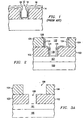
- an overhang 18 of liner/barrier 14 and/or seed 16 material occurs at the top of a trench or via 12 as illustrated in FIG. 1.
- the overhang causes a severe problem during the subsequent copper ECD. Specifically, a seam occurs in the copper fill material.
- One proposed solution for overcoming the above problem uses a pre-sputter etch after the trench and via or contact etch, but before liner/barrier deposition.
- the sputter etch step can deposit copper onto the sidewalls. Copper can then diffuse through the dielectric and cause reliability problems.
- the invention uses a two layer barrier for a via or contact.
- a thin CVD barrier is deposited over a structure including within a via or contact hole.
- a sputter etch is then performed to remove the CVD barrier at the bottom of the via/contact.
- a second barrier is deposited after the sputter etch.
- a metal fill process can then be performed.
- the invention provides an improved interconnect process having low via/contact resistance and improved reliability.
- a via structure 120 formed according to a first embodiment of the invention is shown in FIG. 2.
- Via structure 120 extends through an interlevel dielectric (ILD) 102 and connects between a lower copper interconnect 101 and an upper copper interconnect (trench structure 122).
- Via structure 120 comprises a first barrier/liner 124 located on the sidewalls of the via.
- First barrier/liner 124 does not extend along the bottom surface of the via.
- the thickness of first barrier/liner 124 may be in the range of 25-200 ⁇ .
- first barrier/liner 124 does not extend along the bottom surface of the via, the resistivity of the material used for first barrier/liner 124 is not critical. Accordingly, a wider choice of materials is available.
- a material having good adhesion properties and good barrier properties against copper diffusion should be selected.
- amorphous ternary transition metal-silicon nitrides such as TaSiN, TiSiN, MoSiN or WSiN may be used even though they typically have higher resistivity.
- Dielectrics, such as SiN may also be used.
- the preferred embodiment uses TiSiN deposited by CVD. CVD TiSiN offers excellent adhesion and barrier properties. Copper doesn't diffuse through TiSiN and the silicon bonds easily with the copper at the interface, resulting in good adhesion property.
- Second barrier/liner 126 is located adjacent the first barrier liner 124 on the sidewalls of the via. Second barrier liner 126 does extend along the bottom surface of the via. Accordingly, the resistivity of the second barrier/liner 126 is important. In a preferred embodiment, second barrier liner 126 comprises a lower resistivity material than first barrier/liner 124. For example, PVD transition metals (such as Ta, Ti, Mo and W) or their nitrides such as TaN, TiN, WN, and MoN may be used. The thickness of second barrier/liner 126 is less than the thickness of prior art PVD barrier/liners. For example, the thickness may be in the range of 25-150 ⁇ . This layer is needed to make sure Cu has good adhesion on the upper surface (the first barrier/liner is removed from the upper surface, as will be discussed below).
- PVD transition metals such as Ta, Ti, Mo and W
- the thickness of second barrier/liner 126 is less than the thickness of prior art PVD barrier/liners. For example,
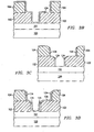
- a method for forming the via structure 120 of FIG. 2 will now be discussed with reference to FIGs. 3A-3F.
- a semiconductor body 100 is processed through formation of trench and vias in a metal interconnect level, as shown in FIG. 3A.
- Semiconductor body 100 typically comprises a silicon substrate with transistors and other devices formed therein.
- Semiconductor body 100 also includes the pre-metal dielectric (PMD) and may include one or more metal interconnect layers. Only copper interconnect 101 is shown.
- PMD pre-metal dielectric
- ILD interlevel dielectric
- IMD intrametal dielectric
- An etchstop layer (not shown) may optionally be placed between ILD 102 and IMD 104.
- Suitable dielectrics for ILD 102 and IMD 104 such as silicon dioxides, fluorine-doped silicate glass (FSG), organo-silicate glass (OSG), hydrogen silesquioxane (HSQ), and combinations thereof, are known in the art.
- ILD 102 and IMD 104 are thick dielectric layers having a thickness in the range of 0.1 um - 1 um.
- both the vias and trenches are etched in the dielectric.
- Via 106 is etched in ILD 102 and trench 108 is etched in IMD 104.
- Via 106 is used to connect to underlying metal interconnect layer 101.
- Trench 108 is used to form the metal interconnect lines.
- First barrier/liner layer 124 is deposited using a CVD process over IMD 104 including in trench 108 and via 106, as shown in FIG. 3B.
- CVD allows a thin conformal layer to be deposited.
- the thickness of first barrier/liner 124 may be in the range of 25 -200 ⁇ .
- a sputter etch is then performed.
- Argon sputtering is used in the preferred embodiment.
- Sputter etching uses a line-of-sight that removes more material on the horizontal surfaces than on the vertical surfaces. Accordingly, the portions of first barrier/liner 124 on the upper surface of IMD 104, the bottom of trench 108, and the bottom of via 106 are removed. The upper corners of via 106 and trench 108 are both also pulled back.
- Sputter-etching at the via bottom functions to breakthrough the barrier 124 and clean the via bottom. Because this exposes the copper from the underlying copper interconnect 101, some copper is sputtered onto the sidewalls of the via. However, the first barrier/liner 124 prevents this copper from diffusing into the dielectric and causing reliability problems.
- first barrier/liner 124 is removed at the bottom of the via, the resistivity of the material used for first barrier/liner 124 is not critical.
- a material having good adhesion properties and good barrier properties against copper diffusion should be selected.
- amorphous ternary transition metal-silicon-nitrides such as TaSiN, TiSiN or WSiN may be used even though they typically have higher resistivity.
- Dielectrics, such as SiN may also be used.
- the preferred embodiment uses TiSiN.
- CVD TiSiN offers excellent adhesion and barrier properties. Copper doesn't diffuse through TiSiN and the silicon bonds easily with the copper at the Cu-barrier interface.
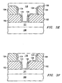
- the second barrier/liner layer 126 is deposited, as shown in FIG. 3D. Either PVD or CVD may be used. The thickness of second barrier/liner layer 126 may be in the range of 25 -150 ⁇ . Because a thin layer is deposited and the top corners of the via and trench are both pulled back during the sputter etch, the overhang of the PVD barrier is not an issue. However, since the second barrier/liner 126 remains at the bottom of the via (i.e., in the electrical path), the resistivity of the second barrier/liner 126 is important. Accordingly, a PVD or CVD process with transition metal or its nitride such as Ta, Ti, Mo, W, TaN, TiN, WN, and MoN may be used.
- transition metal or its nitride such as Ta, Ti, Mo, W, TaN, TiN, WN, and MoN may be used.
- a copper seed layer is deposited over the second barrier/liner layer 126.
- the seed layer is typically deposited using a PVD process.
- Copper ECD is then performed as shown in FIG. 3E to form copper layer 118.
- Various copper ECD processes are known in the art. In one example, a 3-step process is used. After placing the wafer in the plating solution, a current of approximately 0.75 Amps is passed through the seed layer for a time on the order of 15 secs. The current is then increased to around 3 Amps for approximately 60 seconds. Final plating occurs at a current of about 7.5Amps with the duration determined by the final desired thickness.
- a quick spin-rinse dry (SRD) is performed in the plating cell above the plating solution. The wafer is then transferred to the SRD cell and a post-ECD SRD is used to clean the plating residue.
- SRD quick spin-rinse dry
- CMP chemically-mechanically polish
- a semiconductor body 100 is processed through formation of trench 108 and vias 106 in a metal interconnect level. Then, as shown in FIG. 4A a PVD barrier layer 224 is first deposited over the structure including within the trench 108 and via 106. A thickness on the order of 250 ⁇ is used. Since the PVD deposited barrier will remain at the bottom of the via, a low resistivity material is used. For example, ternary transition metal nitride may be used.
- a CVD barrier layer 226 is deposited over the PVD barrier 224.
- the CVD barrier layer 226 has a thickness in the range of 25-100 ⁇ . Because the CVD barrier 226 will be removed at the bottom of the via, resistivity of the material is not critical. A material having good adhesion properties and good barrier properties against copper diffusion should be selected. For example, amorphous ternary transition metal-silicon-nitrides such as TaSiN, TiSiN or WSiN may be used even though the typically have higher resistivity. Dielectrics, such as SiN may also be used. The preferred embodiment uses TiSiN deposited by CVD.
- a sputter etch is performed, as shown in FIG. 4B.
- An inert gas such as argon, may be used.
- the sputter-etch is tuned to remove portions of CVD barrier layer 226 at the bottom of via 106 as well as on the other horizontal surfaces. During this step, the top corners of the trenches and vias are also pulled back to eliminate the overhang that is created during the PVD barrier process (layer 224).
- the second embodiment is less preferred than the first embodiment.
- the sputter etch of the second embodiment is difficult to control.
- Another alternative embodiment of the method of the present invention might comprise: forming a dielectric layer over a semiconductor body; forming a hole in said dielectric layer; depositing a first barrier layer over said dielectric layer including in said hole using physical vapour deposition; depositing a second barrier layer over said first barrier layer using chemical vapour deposition; performing a sputter etch to remove said second barrier layer from a bottom of said hole; and filling said hole with a metal.
- the second barrier layer may comprise silicon nitride or a transition metal-silicon-nitride
- the first barrier layer may comprise a transition metal-nitride.
Landscapes
- Internal Circuitry In Semiconductor Integrated Circuit Devices (AREA)
- Drying Of Semiconductors (AREA)
Applications Claiming Priority (2)
| Application Number | Priority Date | Filing Date | Title |
|---|---|---|---|
| US783157 | 2001-02-14 | ||
| US09/783,157 US6624066B2 (en) | 2001-02-14 | 2001-02-14 | Reliable interconnects with low via/contact resistance |
Publications (3)
| Publication Number | Publication Date |
|---|---|
| EP1233448A2 true EP1233448A2 (fr) | 2002-08-21 |
| EP1233448A3 EP1233448A3 (fr) | 2003-04-23 |
| EP1233448B1 EP1233448B1 (fr) | 2012-05-30 |
Family
ID=25128352
Family Applications (1)
| Application Number | Title | Priority Date | Filing Date |
|---|---|---|---|
| EP02100138A Expired - Lifetime EP1233448B1 (fr) | 2001-02-14 | 2002-02-14 | Interconnexions fiables avec résistance de traversée/contact basse |
Country Status (3)
| Country | Link |
|---|---|
| US (1) | US6624066B2 (fr) |
| EP (1) | EP1233448B1 (fr) |
| JP (1) | JP2002289690A (fr) |
Cited By (5)
| Publication number | Priority date | Publication date | Assignee | Title |
|---|---|---|---|---|
| EP1263035A1 (fr) * | 2001-05-23 | 2002-12-04 | Texas Instruments Incorporated | Procédé de scellement des parois laterales d'une couche diélectrique à faible constante diélectrique |
| GB2394831A (en) * | 2002-09-30 | 2004-05-05 | Agere Systems Inc | A method for preventing contamination of a dielectric |
| WO2005048342A1 (fr) * | 2003-11-08 | 2005-05-26 | Advanced Micro Devices, Inc. | Procede pour empecher l'augmentation de la largeur d'un trou de contact lors de la formation d'un contact |
| WO2005053019A1 (fr) * | 2003-11-28 | 2005-06-09 | International Business Machines Corporation | Procede pour former une interconnexion electroconductrice |
| CN102820255A (zh) * | 2011-06-08 | 2012-12-12 | 无锡华润上华半导体有限公司 | 一种pvd沉积薄膜的方法 |
Families Citing this family (65)
| Publication number | Priority date | Publication date | Assignee | Title |
|---|---|---|---|---|
| US6686280B1 (en) * | 1999-07-22 | 2004-02-03 | Taiwan Semiconductor Manufacturing Company | Sidewall coverage for copper damascene filling |
| US8696875B2 (en) | 1999-10-08 | 2014-04-15 | Applied Materials, Inc. | Self-ionized and inductively-coupled plasma for sputtering and resputtering |
| US10047430B2 (en) | 1999-10-08 | 2018-08-14 | Applied Materials, Inc. | Self-ionized and inductively-coupled plasma for sputtering and resputtering |
| US6764940B1 (en) | 2001-03-13 | 2004-07-20 | Novellus Systems, Inc. | Method for depositing a diffusion barrier for copper interconnect applications |
| US7781327B1 (en) | 2001-03-13 | 2010-08-24 | Novellus Systems, Inc. | Resputtering process for eliminating dielectric damage |
| US7186648B1 (en) | 2001-03-13 | 2007-03-06 | Novellus Systems, Inc. | Barrier first method for single damascene trench applications |
| US8043484B1 (en) | 2001-03-13 | 2011-10-25 | Novellus Systems, Inc. | Methods and apparatus for resputtering process that improves barrier coverage |
| JP3540302B2 (ja) * | 2001-10-19 | 2004-07-07 | Necエレクトロニクス株式会社 | 半導体装置およびその製造方法 |
| US7504006B2 (en) | 2002-08-01 | 2009-03-17 | Applied Materials, Inc. | Self-ionized and capacitively-coupled plasma for sputtering and resputtering |
| US6784096B2 (en) | 2002-09-11 | 2004-08-31 | Applied Materials, Inc. | Methods and apparatus for forming barrier layers in high aspect ratio vias |
| US6949461B2 (en) * | 2002-12-11 | 2005-09-27 | International Business Machines Corporation | Method for depositing a metal layer on a semiconductor interconnect structure |
| KR100523618B1 (ko) * | 2002-12-30 | 2005-10-24 | 동부아남반도체 주식회사 | 반도체 장치의 콘택트 홀 형성 방법 |
| US20040127014A1 (en) * | 2002-12-30 | 2004-07-01 | Cheng-Lin Huang | Method of improving a barrier layer in a via or contact opening |
| US7842605B1 (en) * | 2003-04-11 | 2010-11-30 | Novellus Systems, Inc. | Atomic layer profiling of diffusion barrier and metal seed layers |
| US8298933B2 (en) | 2003-04-11 | 2012-10-30 | Novellus Systems, Inc. | Conformal films on semiconductor substrates |
| US7101785B2 (en) * | 2003-07-22 | 2006-09-05 | Infineon Technologies Ag | Formation of a contact in a device, and the device including the contact |
| US7098537B2 (en) * | 2003-11-21 | 2006-08-29 | International Business Machines Corporation | Interconnect structure diffusion barrier with high nitrogen content |
| US20050146048A1 (en) * | 2003-12-30 | 2005-07-07 | Dubin Valery M. | Damascene interconnect structures |
| US20050266679A1 (en) * | 2004-05-26 | 2005-12-01 | Jing-Cheng Lin | Barrier structure for semiconductor devices |
| US20050263891A1 (en) * | 2004-05-28 | 2005-12-01 | Bih-Huey Lee | Diffusion barrier for damascene structures |
| JP2006120672A (ja) * | 2004-10-19 | 2006-05-11 | Matsushita Electric Ind Co Ltd | 半導体装置及びその製造方法 |
| US20060099802A1 (en) * | 2004-11-10 | 2006-05-11 | Jing-Cheng Lin | Diffusion barrier for damascene structures |
| KR100641362B1 (ko) * | 2005-01-13 | 2006-10-31 | 삼성전자주식회사 | 이중 확산방지막을 갖는 배선구조 및 그 제조방법 |
| US7193327B2 (en) * | 2005-01-25 | 2007-03-20 | Taiwan Semiconductor Manufacturing Company, Ltd. | Barrier structure for semiconductor devices |
| US7135402B2 (en) * | 2005-02-01 | 2006-11-14 | Taiwan Semiconductor Manufacturing Company, Ltd. | Sealing pores of low-k dielectrics using CxHy |
| US7365026B2 (en) * | 2005-02-01 | 2008-04-29 | Taiwan Semiconductor Manufacturing Company, Ltd. | CxHy sacrificial layer for cu/low-k interconnects |
| US7335588B2 (en) * | 2005-04-15 | 2008-02-26 | International Business Machines Corporation | Interconnect structure and method of fabrication of same |
| JP2006324414A (ja) * | 2005-05-18 | 2006-11-30 | Toshiba Corp | 半導体装置及びその製造方法 |
| US8264086B2 (en) | 2005-12-05 | 2012-09-11 | Taiwan Semiconductor Manufacturing Company, Ltd. | Via structure with improved reliability |
| US7781892B2 (en) * | 2005-12-22 | 2010-08-24 | Taiwan Semiconductor Manufacturing Company, Ltd. | Interconnect structure and method of fabricating same |
| US20070259519A1 (en) * | 2006-05-02 | 2007-11-08 | International Business Machines Corporation | Interconnect metallization process with 100% or greater step coverage |
| US20070257366A1 (en) * | 2006-05-03 | 2007-11-08 | Taiwan Semiconductor Manufacturing Company, Ltd. | Barrier layer for semiconductor interconnect structure |
| US7645696B1 (en) | 2006-06-22 | 2010-01-12 | Novellus Systems, Inc. | Deposition of thin continuous PVD seed layers having improved adhesion to the barrier layer |
| US7855147B1 (en) | 2006-06-22 | 2010-12-21 | Novellus Systems, Inc. | Methods and apparatus for engineering an interface between a diffusion barrier layer and a seed layer |
| JP5162869B2 (ja) * | 2006-09-20 | 2013-03-13 | 富士通セミコンダクター株式会社 | 半導体装置およびその製造方法 |
| US7902066B2 (en) * | 2006-09-26 | 2011-03-08 | Chartered Semiconductor Manufacturing, Ltd. | Damascene contact structure for integrated circuits |
| JP4740083B2 (ja) * | 2006-10-05 | 2011-08-03 | 株式会社東芝 | 半導体装置、およびその製造方法 |
| US7510634B1 (en) | 2006-11-10 | 2009-03-31 | Novellus Systems, Inc. | Apparatus and methods for deposition and/or etch selectivity |
| KR100853098B1 (ko) * | 2006-12-27 | 2008-08-19 | 동부일렉트로닉스 주식회사 | 반도체 소자의 금속 배선 및 이의 제조 방법 |
| US7682966B1 (en) | 2007-02-01 | 2010-03-23 | Novellus Systems, Inc. | Multistep method of depositing metal seed layers |
| US7897516B1 (en) | 2007-05-24 | 2011-03-01 | Novellus Systems, Inc. | Use of ultra-high magnetic fields in resputter and plasma etching |
| US7922880B1 (en) | 2007-05-24 | 2011-04-12 | Novellus Systems, Inc. | Method and apparatus for increasing local plasma density in magnetically confined plasma |
| US20080311711A1 (en) * | 2007-06-13 | 2008-12-18 | Roland Hampp | Gapfill for metal contacts |
| US7659197B1 (en) * | 2007-09-21 | 2010-02-09 | Novellus Systems, Inc. | Selective resputtering of metal seed layers |
| DE102007046846A1 (de) * | 2007-09-29 | 2009-04-09 | Advanced Micro Devices, Inc., Sunnyvale | Seitenwandschutzschicht |
| US8017523B1 (en) | 2008-05-16 | 2011-09-13 | Novellus Systems, Inc. | Deposition of doped copper seed layers having improved reliability |
| JP5596919B2 (ja) * | 2008-11-26 | 2014-09-24 | キヤノン株式会社 | 半導体装置の製造方法 |
| DE102009023251B4 (de) * | 2009-05-29 | 2011-02-24 | Globalfoundries Dresden Module One Limited Liability Company & Co. Kg | Verfahren zur Herstellung eines Kontaktelements mit großem Aspektverhältnis und mit einer günstigeren Form in einem Halbleiterbauelement zur Verbesserung der Abscheidung einer Beschichtung |
| JP2010287831A (ja) * | 2009-06-15 | 2010-12-24 | Renesas Electronics Corp | 半導体装置およびその製造方法 |
| US20110217832A1 (en) * | 2009-09-30 | 2011-09-08 | Digvijay Raorane | Method of filling a deep trench in a substrate |
| US8580687B2 (en) * | 2010-09-30 | 2013-11-12 | Infineon Technologies Ag | Semiconductor structure and method for making same |
| US8765546B1 (en) | 2013-06-24 | 2014-07-01 | United Microelectronics Corp. | Method for fabricating fin-shaped field-effect transistor |
| US9536826B1 (en) * | 2015-06-15 | 2017-01-03 | Taiwan Semiconductor Manufacturing Co., Ltd. | Fin field effect transistor (finFET) device structure with interconnect structure |
| US10332790B2 (en) | 2015-06-15 | 2019-06-25 | Taiwan Semiconductor Manufacturing Co., Ltd. | Fin field effect transistor (FinFET) device structure with interconnect structure |
| US9859156B2 (en) * | 2015-12-30 | 2018-01-02 | Taiwan Semiconductor Manufacturing Co., Ltd. | Interconnection structure with sidewall dielectric protection layer |
| US10002789B2 (en) | 2016-03-24 | 2018-06-19 | International Business Machines Corporation | High performance middle of line interconnects |
| US9935051B2 (en) | 2016-08-18 | 2018-04-03 | International Business Machines Corporation | Multi-level metallization interconnect structure |
| US9953864B2 (en) | 2016-08-30 | 2018-04-24 | International Business Machines Corporation | Interconnect structure |
| US10361120B2 (en) | 2017-11-30 | 2019-07-23 | Taiwan Semiconductor Manufacturing Co., Ltd. | Conductive feature formation and structure |
| DE102018102448B4 (de) | 2017-11-30 | 2023-06-15 | Taiwan Semiconductor Manufacturing Co., Ltd. | Bildung und Struktur leitfähiger Merkmale |
| US10867943B2 (en) * | 2018-06-15 | 2020-12-15 | Taiwan Semiconductor Manufacturing Company, Ltd. | Die structure, die stack structure and method of fabricating the same |
| CN108831859A (zh) * | 2018-06-15 | 2018-11-16 | 武汉新芯集成电路制造有限公司 | 通孔的制造方法 |
| US10832946B1 (en) | 2019-04-24 | 2020-11-10 | International Business Machines Corporation | Recessed interconnet line having a low-oxygen cap for facilitating a robust planarization process and protecting the interconnect line from downstream etch operations |
| JP7574558B2 (ja) | 2020-07-13 | 2024-10-29 | 富士電機株式会社 | 半導体装置 |
| JP7307038B2 (ja) | 2020-09-23 | 2023-07-11 | 株式会社Kokusai Electric | 半導体装置の製造方法、プログラム、基板処理装置および基板処理方法 |
Family Cites Families (12)
| Publication number | Priority date | Publication date | Assignee | Title |
|---|---|---|---|---|
| US5933753A (en) | 1996-12-16 | 1999-08-03 | International Business Machines Corporation | Open-bottomed via liner structure and method for fabricating same |
| US5985762A (en) | 1997-05-19 | 1999-11-16 | International Business Machines Corporation | Method of forming a self-aligned copper diffusion barrier in vias |
| JPH11317446A (ja) * | 1998-05-01 | 1999-11-16 | Mitsubishi Electric Corp | 半導体装置およびその製造方法 |
| US6287977B1 (en) * | 1998-07-31 | 2001-09-11 | Applied Materials, Inc. | Method and apparatus for forming improved metal interconnects |
| JP2000150647A (ja) * | 1998-11-11 | 2000-05-30 | Sony Corp | 配線構造およびその製造方法 |
| TW404007B (en) * | 1998-12-16 | 2000-09-01 | United Microelectronics Corp | The manufacture method of interconnects |
| US6156648A (en) * | 1999-03-10 | 2000-12-05 | United Microelectronics Corp. | Method for fabricating dual damascene |
| JP2000323571A (ja) * | 1999-05-14 | 2000-11-24 | Sony Corp | 半導体装置の製造方法 |
| US6211069B1 (en) * | 1999-05-17 | 2001-04-03 | Taiwan Semiconductor Manufacturing Company | Dual damascene process flow for a deep sub-micron technology |
| US6177347B1 (en) | 1999-07-02 | 2001-01-23 | Taiwan Semiconductor Manufacturing Company | In-situ cleaning process for Cu metallization |
| US6284657B1 (en) * | 2000-02-25 | 2001-09-04 | Chartered Semiconductor Manufacturing Ltd. | Non-metallic barrier formation for copper damascene type interconnects |
| US6498091B1 (en) * | 2000-11-01 | 2002-12-24 | Applied Materials, Inc. | Method of using a barrier sputter reactor to remove an underlying barrier layer |
-
2001
- 2001-02-14 US US09/783,157 patent/US6624066B2/en not_active Expired - Lifetime
-
2002
- 2002-01-18 JP JP2002009630A patent/JP2002289690A/ja active Pending
- 2002-02-14 EP EP02100138A patent/EP1233448B1/fr not_active Expired - Lifetime
Cited By (10)
| Publication number | Priority date | Publication date | Assignee | Title |
|---|---|---|---|---|
| EP1263035A1 (fr) * | 2001-05-23 | 2002-12-04 | Texas Instruments Incorporated | Procédé de scellement des parois laterales d'une couche diélectrique à faible constante diélectrique |
| GB2394831A (en) * | 2002-09-30 | 2004-05-05 | Agere Systems Inc | A method for preventing contamination of a dielectric |
| GB2394831B (en) * | 2002-09-30 | 2006-01-18 | Agere Systems Inc | Method to avoid copper contamination of a via or dual damascene structure |
| US7005375B2 (en) | 2002-09-30 | 2006-02-28 | Agere Systems Inc. | Method to avoid copper contamination of a via or dual damascene structure |
| WO2005048342A1 (fr) * | 2003-11-08 | 2005-05-26 | Advanced Micro Devices, Inc. | Procede pour empecher l'augmentation de la largeur d'un trou de contact lors de la formation d'un contact |
| US7005387B2 (en) | 2003-11-08 | 2006-02-28 | Advanced Micro Devices, Inc. | Method for preventing an increase in contact hole width during contact formation |
| GB2423635A (en) * | 2003-11-08 | 2006-08-30 | Advanced Micro Devices Inc | Method for preventing an increase in contact hole width during contact formation |
| GB2423635B (en) * | 2003-11-08 | 2007-05-30 | Advanced Micro Devices Inc | Method for preventing an increase in contact hole width during contact formation |
| WO2005053019A1 (fr) * | 2003-11-28 | 2005-06-09 | International Business Machines Corporation | Procede pour former une interconnexion electroconductrice |
| CN102820255A (zh) * | 2011-06-08 | 2012-12-12 | 无锡华润上华半导体有限公司 | 一种pvd沉积薄膜的方法 |
Also Published As
| Publication number | Publication date |
|---|---|
| EP1233448B1 (fr) | 2012-05-30 |
| JP2002289690A (ja) | 2002-10-04 |
| US6624066B2 (en) | 2003-09-23 |
| US20020110999A1 (en) | 2002-08-15 |
| EP1233448A3 (fr) | 2003-04-23 |
Similar Documents
| Publication | Publication Date | Title |
|---|---|---|
| EP1233448B1 (fr) | Interconnexions fiables avec résistance de traversée/contact basse | |
| US7365001B2 (en) | Interconnect structures and methods of making thereof | |
| US6566258B1 (en) | Bi-layer etch stop for inter-level via | |
| US6417094B1 (en) | Dual-damascene interconnect structures and methods of fabricating same | |
| US7041595B2 (en) | Method of forming a barrier seed layer with graded nitrogen composition | |
| US6174811B1 (en) | Integrated deposition process for copper metallization | |
| US20020058409A1 (en) | Elimination of overhang in liner/barrier/seed layers using post-deposition sputter etch | |
| US6740580B1 (en) | Method to form copper interconnects by adding an aluminum layer to the copper diffusion barrier | |
| US6265313B1 (en) | Method of manufacturing copper interconnect | |
| US20060024953A1 (en) | Dual damascene diffusion barrier/liner process with selective via-to-trench-bottom recess | |
| US20020055256A1 (en) | Reducing copper line resistivity by smoothing trench and via sidewalls | |
| US7037835B2 (en) | Interconnections having double capping layer and method for forming the same | |
| US6583053B2 (en) | Use of a sacrificial layer to facilitate metallization for small features | |
| US7037837B2 (en) | Method of fabricating robust nucleation/seed layers for subsequent deposition/fill of metallization layers | |
| US20090096103A1 (en) | Semiconductor device and method for forming barrier metal layer thereof | |
| CN116130411B (zh) | 一种具备防止铜扩散结构的半导体制造方法 | |
| US7589021B2 (en) | Copper metal interconnection with a local barrier metal layer | |
| US6531780B1 (en) | Via formation in integrated circuit interconnects | |
| US7309651B2 (en) | Method for improving reliability of copper interconnects | |
| US20020001944A1 (en) | In-situ co-deposition of Si iN diffusion barrier material depositions with improved wettability, barrier efficiency, and device reliability | |
| US6724087B1 (en) | Laminated conductive lines and methods of forming the same | |
| US7538024B2 (en) | Method of fabricating a dual-damascene copper structure | |
| KR100462762B1 (ko) | 반도체 소자의 구리 배선 형성 방법 | |
| US20040118692A1 (en) | Plating-rinse-plating process for fabricating copper interconnects | |
| JP2000340565A (ja) | 半導体集積回路装置およびその製造方法 |
Legal Events
| Date | Code | Title | Description |
|---|---|---|---|
| PUAI | Public reference made under article 153(3) epc to a published international application that has entered the european phase |
Free format text: ORIGINAL CODE: 0009012 |
|
| AK | Designated contracting states |
Kind code of ref document: A2 Designated state(s): AT BE CH CY DE DK ES FI FR GB GR IE IT LI LU MC NL PT SE TR |
|
| AX | Request for extension of the european patent |
Free format text: AL;LT;LV;MK;RO;SI |
|
| PUAL | Search report despatched |
Free format text: ORIGINAL CODE: 0009013 |
|
| AK | Designated contracting states |
Designated state(s): AT BE CH CY DE DK ES FI FR GB GR IE IT LI LU MC NL PT SE TR |
|
| AX | Request for extension of the european patent |
Extension state: AL LT LV MK RO SI |
|
| 17P | Request for examination filed |
Effective date: 20031023 |
|
| AKX | Designation fees paid |
Designated state(s): DE FR GB |
|
| 17Q | First examination report despatched |
Effective date: 20040105 |
|
| GRAP | Despatch of communication of intention to grant a patent |
Free format text: ORIGINAL CODE: EPIDOSNIGR1 |
|
| GRAS | Grant fee paid |
Free format text: ORIGINAL CODE: EPIDOSNIGR3 |
|
| GRAA | (expected) grant |
Free format text: ORIGINAL CODE: 0009210 |
|
| AK | Designated contracting states |
Kind code of ref document: B1 Designated state(s): DE FR GB |
|
| REG | Reference to a national code |
Ref country code: GB Ref legal event code: FG4D |
|
| REG | Reference to a national code |
Ref country code: DE Ref legal event code: R096 Ref document number: 60243022 Country of ref document: DE Effective date: 20120802 |
|
| PLBE | No opposition filed within time limit |
Free format text: ORIGINAL CODE: 0009261 |
|
| STAA | Information on the status of an ep patent application or granted ep patent |
Free format text: STATUS: NO OPPOSITION FILED WITHIN TIME LIMIT |
|
| 26N | No opposition filed |
Effective date: 20130301 |
|
| REG | Reference to a national code |
Ref country code: DE Ref legal event code: R097 Ref document number: 60243022 Country of ref document: DE Effective date: 20130301 |
|
| REG | Reference to a national code |
Ref country code: FR Ref legal event code: PLFP Year of fee payment: 15 |
|
| REG | Reference to a national code |
Ref country code: FR Ref legal event code: PLFP Year of fee payment: 16 |
|
| PGFP | Annual fee paid to national office [announced via postgrant information from national office to epo] |
Ref country code: DE Payment date: 20170227 Year of fee payment: 16 Ref country code: FR Payment date: 20170118 Year of fee payment: 16 |
|
| PGFP | Annual fee paid to national office [announced via postgrant information from national office to epo] |
Ref country code: GB Payment date: 20170126 Year of fee payment: 16 |
|
| REG | Reference to a national code |
Ref country code: DE Ref legal event code: R119 Ref document number: 60243022 Country of ref document: DE |
|
| GBPC | Gb: european patent ceased through non-payment of renewal fee |
Effective date: 20180214 |
|
| REG | Reference to a national code |
Ref country code: FR Ref legal event code: ST Effective date: 20181031 |
|
| PG25 | Lapsed in a contracting state [announced via postgrant information from national office to epo] |
Ref country code: DE Free format text: LAPSE BECAUSE OF NON-PAYMENT OF DUE FEES Effective date: 20180901 |
|
| PG25 | Lapsed in a contracting state [announced via postgrant information from national office to epo] |
Ref country code: GB Free format text: LAPSE BECAUSE OF NON-PAYMENT OF DUE FEES Effective date: 20180214 Ref country code: FR Free format text: LAPSE BECAUSE OF NON-PAYMENT OF DUE FEES Effective date: 20180228 |