EP1233455B1 - Cellule de mémoire non-volatile, procédé de fabrication et programmation - Google Patents
Cellule de mémoire non-volatile, procédé de fabrication et programmation Download PDFInfo
- Publication number
- EP1233455B1 EP1233455B1 EP02002386A EP02002386A EP1233455B1 EP 1233455 B1 EP1233455 B1 EP 1233455B1 EP 02002386 A EP02002386 A EP 02002386A EP 02002386 A EP02002386 A EP 02002386A EP 1233455 B1 EP1233455 B1 EP 1233455B1
- Authority
- EP
- European Patent Office
- Prior art keywords
- layer
- charge
- semiconductor memory
- memory cell
- insulating layer
- Prior art date
- Legal status (The legal status is an assumption and is not a legal conclusion. Google has not performed a legal analysis and makes no representation as to the accuracy of the status listed.)
- Expired - Lifetime
Links
- 239000004065 semiconductor Substances 0.000 title claims description 96
- 238000004519 manufacturing process Methods 0.000 title description 10
- 238000000034 method Methods 0.000 claims description 32
- 229910052771 Terbium Inorganic materials 0.000 claims description 31
- 229910052715 tantalum Inorganic materials 0.000 claims description 31
- 239000000758 substrate Substances 0.000 claims description 14
- 239000002800 charge carrier Substances 0.000 claims description 12
- 230000036961 partial effect Effects 0.000 claims description 9
- 238000000059 patterning Methods 0.000 claims description 6
- 238000002347 injection Methods 0.000 claims description 4
- 239000007924 injection Substances 0.000 claims description 4
- 239000000463 material Substances 0.000 claims description 4
- 238000005468 ion implantation Methods 0.000 claims description 2
- 239000007769 metal material Substances 0.000 claims description 2
- FGUUSXIOTUKUDN-IBGZPJMESA-N C1(=CC=CC=C1)N1C2=C(NC([C@H](C1)NC=1OC(=NN=1)C1=CC=CC=C1)=O)C=CC=C2 Chemical compound C1(=CC=CC=C1)N1C2=C(NC([C@H](C1)NC=1OC(=NN=1)C1=CC=CC=C1)=O)C=CC=C2 FGUUSXIOTUKUDN-IBGZPJMESA-N 0.000 claims 1
- 238000002161 passivation Methods 0.000 claims 1
- 238000007667 floating Methods 0.000 description 7
- 238000011156 evaluation Methods 0.000 description 6
- 238000002955 isolation Methods 0.000 description 6
- 238000003860 storage Methods 0.000 description 6
- 230000000670 limiting effect Effects 0.000 description 5
- 230000008878 coupling Effects 0.000 description 4
- 238000010168 coupling process Methods 0.000 description 4
- 238000005859 coupling reaction Methods 0.000 description 4
- 238000010586 diagram Methods 0.000 description 4
- 239000011159 matrix material Substances 0.000 description 4
- 238000005516 engineering process Methods 0.000 description 3
- 238000005530 etching Methods 0.000 description 3
- 229910021420 polycrystalline silicon Inorganic materials 0.000 description 3
- 229920005591 polysilicon Polymers 0.000 description 3
- VYPSYNLAJGMNEJ-UHFFFAOYSA-N Silicium dioxide Chemical compound O=[Si]=O VYPSYNLAJGMNEJ-UHFFFAOYSA-N 0.000 description 2
- XUIMIQQOPSSXEZ-UHFFFAOYSA-N Silicon Chemical compound [Si] XUIMIQQOPSSXEZ-UHFFFAOYSA-N 0.000 description 2
- 230000015572 biosynthetic process Effects 0.000 description 2
- 230000005669 field effect Effects 0.000 description 2
- 238000002513 implantation Methods 0.000 description 2
- 238000005457 optimization Methods 0.000 description 2
- 238000001020 plasma etching Methods 0.000 description 2
- 239000005368 silicate glass Substances 0.000 description 2
- 229910052710 silicon Inorganic materials 0.000 description 2
- 239000010703 silicon Substances 0.000 description 2
- 125000006850 spacer group Chemical group 0.000 description 2
- RYGMFSIKBFXOCR-UHFFFAOYSA-N Copper Chemical compound [Cu] RYGMFSIKBFXOCR-UHFFFAOYSA-N 0.000 description 1
- ATJFFYVFTNAWJD-UHFFFAOYSA-N Tin Chemical compound [Sn] ATJFFYVFTNAWJD-UHFFFAOYSA-N 0.000 description 1
- 230000004913 activation Effects 0.000 description 1
- 230000002411 adverse Effects 0.000 description 1
- 229910052782 aluminium Inorganic materials 0.000 description 1
- XAGFODPZIPBFFR-UHFFFAOYSA-N aluminium Chemical compound [Al] XAGFODPZIPBFFR-UHFFFAOYSA-N 0.000 description 1
- 229910021417 amorphous silicon Inorganic materials 0.000 description 1
- 239000000969 carrier Substances 0.000 description 1
- 238000005234 chemical deposition Methods 0.000 description 1
- 229910052802 copper Inorganic materials 0.000 description 1
- 239000010949 copper Substances 0.000 description 1
- 230000003247 decreasing effect Effects 0.000 description 1
- 230000000694 effects Effects 0.000 description 1
- 239000011521 glass Substances 0.000 description 1
- 239000002784 hot electron Substances 0.000 description 1
- 238000009413 insulation Methods 0.000 description 1
- 229910052751 metal Inorganic materials 0.000 description 1
- 239000002184 metal Substances 0.000 description 1
- 239000000203 mixture Substances 0.000 description 1
- 150000004767 nitrides Chemical class 0.000 description 1
- 238000005498 polishing Methods 0.000 description 1
- 230000000171 quenching effect Effects 0.000 description 1
- 230000002829 reductive effect Effects 0.000 description 1
- 235000012239 silicon dioxide Nutrition 0.000 description 1
- 239000000377 silicon dioxide Substances 0.000 description 1
- 239000000126 substance Substances 0.000 description 1
- WQJQOUPTWCFRMM-UHFFFAOYSA-N tungsten disilicide Chemical compound [Si]#[W]#[Si] WQJQOUPTWCFRMM-UHFFFAOYSA-N 0.000 description 1
- 229910021342 tungsten silicide Inorganic materials 0.000 description 1
- 230000005641 tunneling Effects 0.000 description 1
- 238000001039 wet etching Methods 0.000 description 1
Images



Classifications
-
- G—PHYSICS
- G11—INFORMATION STORAGE
- G11C—STATIC STORES
- G11C16/00—Erasable programmable read-only memories
- G11C16/02—Erasable programmable read-only memories electrically programmable
- G11C16/04—Erasable programmable read-only memories electrically programmable using variable threshold transistors, e.g. FAMOS
- G11C16/0408—Erasable programmable read-only memories electrically programmable using variable threshold transistors, e.g. FAMOS comprising cells containing floating gate transistors
- G11C16/0441—Erasable programmable read-only memories electrically programmable using variable threshold transistors, e.g. FAMOS comprising cells containing floating gate transistors comprising cells containing multiple floating gate devices, e.g. separate read-and-write FAMOS transistors with connected floating gates
-
- H—ELECTRICITY
- H10—SEMICONDUCTOR DEVICES; ELECTRIC SOLID-STATE DEVICES NOT OTHERWISE PROVIDED FOR
- H10B—ELECTRONIC MEMORY DEVICES
- H10B41/00—Electrically erasable-and-programmable ROM [EEPROM] devices comprising floating gates
- H10B41/30—Electrically erasable-and-programmable ROM [EEPROM] devices comprising floating gates characterised by the memory core region
-
- H—ELECTRICITY
- H10—SEMICONDUCTOR DEVICES; ELECTRIC SOLID-STATE DEVICES NOT OTHERWISE PROVIDED FOR
- H10B—ELECTRONIC MEMORY DEVICES
- H10B43/00—EEPROM devices comprising charge-trapping gate insulators
- H10B43/30—EEPROM devices comprising charge-trapping gate insulators characterised by the memory core region
-
- H—ELECTRICITY
- H10—SEMICONDUCTOR DEVICES; ELECTRIC SOLID-STATE DEVICES NOT OTHERWISE PROVIDED FOR
- H10B—ELECTRONIC MEMORY DEVICES
- H10B69/00—Erasable-and-programmable ROM [EPROM] devices not provided for in groups H10B41/00 - H10B63/00, e.g. ultraviolet erasable-and-programmable ROM [UVEPROM] devices
-
- H—ELECTRICITY
- H10—SEMICONDUCTOR DEVICES; ELECTRIC SOLID-STATE DEVICES NOT OTHERWISE PROVIDED FOR
- H10D—INORGANIC ELECTRIC SEMICONDUCTOR DEVICES
- H10D30/00—Field-effect transistors [FET]
- H10D30/60—Insulated-gate field-effect transistors [IGFET]
- H10D30/68—Floating-gate IGFETs
- H10D30/6891—Floating-gate IGFETs characterised by the shapes, relative sizes or dispositions of the floating gate electrode
Definitions
- the present invention relates to an information-redundant nonvolatile semiconductor memory cell, and a method of manufacturing and programming the same, and more particularly, to a nonvolatile semiconductor memory cell having two memory elements.
- Rewritable nonvolatile semiconductor memory cells are becoming increasingly important in highly integrated circuits, since they can store, for example, data that can be changed into smart cards over a long period of time and without the use of a power supply.
- FIG. 1 shows a conventional FLASH single-transistor cell, after which in an active region of a semiconductor substrate 10, source and drain regions (S / D) are formed for defining a channel region.
- source and drain regions S / D
- an erased state is a state in which, for example, many electrons are present in the floating gate layer 30.
- the threshold voltage of the cell transistor is shifted to high values.
- memory cells are referred to as programmed if, for example, there is a lack of electrons in the floating gate layer 30 and consequently the threshold voltage of the transistor is lowered.
- the erased (high threshold voltage) or programmed (low threshold voltage) state is checked by evaluating a current I between source and drain against a fixed limit. Specifically, this means that for an erased memory cell, an upper current limit I erase exists, and a memory cell is considered erased only when that cell provides a lower current when reading. In contrast, there is a lower current limit I prog for programmed memory cells, the memory cell being considered programmed only if it supplies more current than this limiting current during reading.
- the limiting current I erase is greater than the limiting current I prog , wherein a difference between these limiting currents can be the smaller, the more sensitive an evaluation circuit or sense amplifier is the more time is available for reading.
- a fundamental feature of conventional nonvolatile semiconductor memory cells is that as the number of program / erase cycles increases, the threshold voltages of the erased and programmed states approximate each other as "holes" are partially built into the tunnel oxide layer 20 during the erase and program. The achieved shifts of the threshold voltage are decreasing more and more, so that the threshold voltage of the erased and the programmed state converge with increasing number of cycles, ie number of program / erase cycles, to the UV-erased state, which is characterized no charge is stored in the floating gate layer 30.
- the number of program / erase cycles or so-called endurance of conventional non-volatile semiconductor memory cells is consequently limited by the fact that either the erased or the programmed state no longer meets the evaluation criteria for the limiting current.
- a multibit semiconductor memory cell which has two separate and adjacent memory layers along a channel.
- the storage layers are separated from each other by a spacer and a tunnel layer. This allows for three different levels of output by varying the effective channel length, depending on whether one or both of the memory layers are programmed or erased.
- the publication US-A-5 757 044 discloses another conventional semiconductor memory cell wherein, to avoid an over-erase effect, a plurality of charge-trapping layers are disposed along a channel of the memory element and isolated from each other.
- EP-A-0 443 515 For example, a conventional nonvolatile flash memory device is known wherein a plurality of nonvolatile semiconductor memory cells are arranged in a matrix. To improve the quenching properties with simultaneously improved electrical properties of the gate oxide, an erase electrode is flanged laterally over a tunnel oxide to the charge-storing layer.
- the invention is based on the object to provide an information-redundant non-volatile semiconductor memory cell, as well as methods for their production and programming, which has an increased data security and improved Endurance or cycle life.
- first and second non-volatile memory element with respective source / drain regions and with a respective charge-storing layer, wherein the charge-storing layers are coupled together via a tunnel insulating layer such that a charge exchange between the memory elements is made possible
- a relative evaluation of the channel currents of the memory elements to each other a much higher program / erase number of cycles.
- absolute evaluation moreover, increased data security can be realized since the stored information is in each case redundantly present in the two nonvolatile memory elements and if one memory element still fails, the information of the other memory element is still available for evaluation.
- the tunnel insulating layer preferably has a tunnel oxide and is arranged either perpendicular and / or parallel to the substrate surface.
- an OTP layer is preferably used for the one-time programming of the nonvolatile memory elements, whereby an introduction of charge carriers or a precharging can be carried out, for example by an electrical control or else process technology, for example by setting a respective plasma density in the etching process.
- charge-storing layers preferably electrically conductive semiconductor layers and in particular highly doped amorphous semiconductor layers are used, resulting in a particularly simple production of these layers and the tunnel insulating layer.
- a second insulating layer preferably consists of an ONO layer sequence, whereby the production is greatly simplified and the costs are reduced.
- a preferred method for precharging the information redundant nonvolatile semiconductor memory cell first applying a first positive precharge voltage to the control layers of the nonvolatile semiconductor memory cell and then applying a second precharge voltage smaller than the first precharge voltage to the source / drain regions of the memory elements are applied in that charge carriers are introduced into the charge-storing layers by means of Fowler-Nordheim tunnels.
- precharging may also be performed by applying a first positive precharge voltage to the control layers of the nonvolatile semiconductor memory cell, applying a second precharge voltage smaller than the first precharge voltage to the source regions, and applying a third Precharge voltage, which is smaller than the first precharge voltage but greater than the second precharge voltage, to the drain regions of the memory elements carried out such that charge carriers are introduced by channel injection or injection of hot electrons in the charge storage layers.
- the nonvolatile semiconductor memory cell For reading the nonvolatile semiconductor memory cell is preferably a first negative read voltage to the control layers of the memory elements for selecting a semiconductor memory cell, further, a second read voltage which is greater than the first read voltage to the source regions of the first and second memory element, a third read voltage, the larger as the second read voltage is applied to the drain regions of the first and second memory elements and then comparing the channel currents of the first and second memory elements. Accordingly, even with a high charge loss, for example due to leakage currents or a strong shift of the threshold voltage due to holes in the tunnel oxide layer, an informational state of the semiconductor memory cell can be unambiguously evaluated for a very long time.
- FIG. 2 shows a simplified sectional view of an information-redundant non-volatile semiconductor memory cell according to a first embodiment, wherein in a semiconductor substrate 1 such as a silicon semiconductor substrate active areas AA, for example, by shallow trench isolation STI (shallow trench isolation) are formed. In the active areas AA also not shown source and drain areas for the realization of a field effect transistor, for example, by implantation or other doping are formed.
- the information-redundant nonvolatile semiconductor memory cell essentially consists of a first nonvolatile memory element Ta and a second nonvolatile memory element Tb, for example, the structure of the FLASH single transistor memory cell according to FIG. 1 can have. However, they are not limited thereto and may include other memory elements with, for example, a separate tunnel window and the like.
- the first non-volatile memory element Ta consists of a layer sequence of a first insulating layer 2, a charge-storing layer 3a, a second insulating layer 4a and a control layer 5a, which are located above a channel region formed in the active region AA.
- the second nonvolatile memory element Tb consists of a first insulating layer 2, a charge storing layer 3b, a second insulating layer 4b and a control layer 5b.
- the basic mode of operation of this semiconductor memory cell in this case requires a precharge process in which initially a certain number of charge carriers in one or both charge-storing layers 3a and 3b is introduced via the first insulating layer 2.
- This defined precharging of the charge-storing layers 3a and 3b can take place, for example, via electrical activation of the respective source and drain regions as well as the control layers of the memory elements.
- it can also be realized in terms of process technology already during a production process, wherein, for example, a plasma density is varied in an etching process and thus a charge or a number of charge carriers in the charge-storing layer 3a and 3b can be set.
- An endurance or number of program / erase cycles can thus be substantially increased because, on the one hand, a quality of the first insulating layer is not adversely affected by the program / erase operations and, further, only one charge shift across the tunnel insulating layer between the charge-storing layers 3a and 3b takes place.
- such an information redundant nonvolatile semiconductor memory cell offers a further advantage in that it enables a particularly high data security. More specifically, using the same type of semiconductor memory cell and using an alternative evaluation circuit, data security as required particularly in smart cards as well as in the automotive and avionics field can be realized.
- the information units stored in the respective storage elements Ta and Tb which are symmetrical to each other are not compared with each other, but evaluated against a fixed reference value as in the prior art. If one of the memory elements Ta or Tb is damaged due to damage, e.g. fails in the insulating layers or conductive layers, the information content of the memory cell can continue to be determined via the redundant memory element. Due to the double field of use of such information-redundant semiconductor memory cell, consequently, the production costs decrease considerably due to the higher market volume.
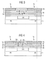
- FIG. 3 shows a simplified sectional view of an information redundant nonvolatile semiconductor memory cell according to a second embodiment, wherein like reference numerals designate the same or similar layers and a repeated description is omitted below.
- the first and second memory elements Ta and Tb again consist of a layer sequence of a first insulating layer 2, a charge-storing layer 3a and 3b, a second insulating layer 4 and a control layer 5a and 5b.
- the tunnel insulating layer is formed over the entire surface and then the charge-storing layer 3b of the second memory element Tb is overlapped over it.
- the second insulating layer 4 consists of a single full-surface dielectric coupling layer. It can, however, like in FIG. 2 also consist of separate layers.
- FIG. 4 shows a simplified sectional view of an information redundant nonvolatile semiconductor memory cell according to a third embodiment, wherein like reference numerals the same or similar layers as in Figures 2 and 3 denote and a repeated description is omitted below.
- the tunnel insulating layer 2 ' may be formed only in a region substantially parallel to the substrate surface between the first and second charge-trapping layers 3a and 3b, in which case after formation and patterning of the charge-trapping layer 3a of the first storage element Ta, sidewall isolation is provided Sia is trained. Subsequently the tunnel insulating layer 2 'is formed on the surface of the charge-storing layer 3a with a subsequent structuring. Finally, the charge-storing layer 3b is partially overlapped and formed over the tunnel insulating layer 2 'or the charge-storing layer 3a and also provided with a sidewall insulation Sib. In this way, a semiconductor memory cell having improved leakage characteristics is obtained.
- the second insulating layer consist of a respective insulating layer 4a and 4b for the first and second memory elements Ta and Tb, but different first insulating layers 2a and 2b for the respective memory elements can also be used for the first insulating layer.
- a particularly high-quality tunnel oxide can be used in this way only on one side or for a memory element for the one-time programming or pre-charging of the semiconductor memory cell.
- FIG. 5 Here, a simplified plan view of an information redundant non-volatile semiconductor memory cell according to the fourth embodiment and FIG. 6 a simplified sectional view of this semiconductor memory cell along a section I-I '.
- the same reference numerals here again designate the same or similar layers or elements, for which reason a repeated description is omitted below.
- active regions AA are preferably formed in a semiconductor substrate 1 by means of shallow trench isolation STI (shallow trench isolation). However, the active areas AA can also be used with other isolation methods be formed in the semiconductor substrate 1.
- a first insulating layer 2 is formed over the entire surface, wherein preferably an OTP layer is used for the one-time programming of the nonvolatile memory elements.
- This OTP layer consists for example of a thermally formed silicon dioxide, which is why it assumes a relevant thickness only above the active areas AA.
- other insulating layers and in particular high-quality gate oxides may be formed as first insulating layers.
- a charge-storing layer 3a is formed over the entire surface and structured such that it represents a charge-storing layer 3a for a first storage element Ta.
- an electrically conductive amorphous silicon layer is deposited for this charge-storing layer.
- the above-described pre-charging of the semiconductor memory cell can be performed by adjusting a respective plasma density.
- a tunnel insulating layer 2 ' is preferably thermally formed using a conventional furnace process or a rapid thermal process (RTP). According to FIG. 6 the thus formed tunnel insulating layer 2 ', which represents, for example, a thermally formed tunnel oxide, recessed substantially perpendicular to the substrate surface, but also in the FIGS. 2 to 4 possible basic arrangements are conceivable.
- charge-storing layer for realizing the charge-storing layer 3b is formed and patterned, wherein in turn, for example, electrically conductive amorphous semiconductor material (Si) or insitu-doped polysilicon is deposited.
- Si electrically conductive amorphous semiconductor material
- insitu-doped polysilicon is deposited.
- CMP chemical mechanical polishing
- a second insulating layer 4 is formed over the entire surface, wherein, for example, an ONO layer sequence (oxide / nitride / oxide) is formed as a coupling dielectric.
- ONO layer sequence oxide / nitride / oxide
- dielectric layers of high relative dielectric constant may also be used, e.g. TiN, ..., whereby a coupling factor for reducing the programming voltages can be improved.
- an electrically conductive layer is formed and patterned, the respective control layers 5a and 5b or the word lines WLa and WLb of the first and second memory elements Ta and Tb being realized.
- highly doped semiconductor material and / or metallic material can be used as the material for the electrically conductive control layers.
- highly doped polysilicon, tungsten silicide or a metal is preferably used for the control layers 5a and 5b.
- first and second insulating layers 2 and 4 and the first and second charge-storing layer 3a and 3b are used by using the patterned control layers 5a and 5b, the second insulating layer 4, the charge-storing layer 3a and 3b, and the first insulating layer 2 are self-aligned as a mask by means of ion implantation.
- LDD region as well as spacers can be formed on the respective word line stacks.
- a third insulating layer 6 for example, BPSG (boron-phosphorous-silicate glass), PSG (phosphorous-silicate glass) or APUSG (atmoshperic pressure undoped silicon glass) is formed by means of, for example, HDP, PE, or LP-chemical deposition.
- contact holes are then etched free to the respective source regions Sa, Sb and drain regions Da, Db of the memory elements Ta and Tb and filled to form contacts K, for example with W, poly, aluminum, copper and so on.
- bit line layer 7 is formed and structured to realize bit lines BLDa, BLSa, BLSb and BLDb for the first and second memory elements Ta and Tb.
- the bit lines lie substantially above the active areas AA and cross the word lines WL to realize a matrix-shaped memory device.
- FIG. 7 shows an electrical equivalent circuit diagram of the inventive information redundant nonvolatile semiconductor memory cell SZ wherein the same reference numerals again denote the same or similar elements and is omitted a repeated description below.
- the non-volatile semiconductor memory cell SZ consists of two nonvolatile memory elements Ta and Tb, whose charge-storing layers are coupled to each other via the tunnel insulating layer 2 '. Respective channel currents Ia and Ib can be compared to each other to improve Endurance. Alternatively, however, to improve data security, a respective channel current Ia and Ib of the memory elements Ta and Tb in each case opposite be evaluated a fixed reference value, wherein even if information is lost in a memory element, the information of the semiconductor memory cell via the other memory element can be reliably determined. In particular, the required in smart cards and in the automotive and aircraft high demands for data security can be reliably met with this type of semiconductor memory cell.
- FIG. 8 shows a simplified block diagram of a matrix arrangement of the non-volatile semiconductor memory cells described above, wherein like reference numerals again denote the same or similar elements and is omitted a repeated description below.
- the information redundant nonvolatile semiconductor memory cells SZ are arranged in the form of a matrix and are driven in rows or columns via word lines WL1 to WL3 and bit lines BL1 to BL3.
- the bit lines in this case each consist of four partial bit lines BLSa, BLDa, BLSb and BLDb for driving the respective source and drain regions.
- the word lines consist of partial word lines CGa and CGb for driving the respective control layers 5a and 5b of the nonvolatile memory elements Ta and Tb.
- a predetermined number of charge carriers are initially stored on the common floating gate or the common charge-storing layers. More specifically, let the sum of the number of carriers on the charge-trapping layer 3a and the charge-trapping layer 3b of the first and second memory element for all semiconductor memory cells SZ be constant.
- essentially two methods for electrically driving the semiconductor memory cells are available for this initialization.
- a voltage of +20 V is applied to the control layers 5a and 5b and the partial word lines CGa and CGb, respectively.
- the partial bit lines BLSa, BLDa, BLSb and BLDb and the associated source and drain regions Sa, Da, Sb, Db in this case have a potential of 0 V.
- such precharging or introduction of a predetermined number of charge carriers into the charge-storing layers can also take place by means of injection of hot channel electrons via the first insulating layer 2.
- the partial word line CGa and CGb and the associated control layers 5a and 5b are set to +12 V, while the voltages of the source regions Sa and Sb are 0 V and the voltages of the associated drain regions Da and Db have 7V.
- the charge-storing layer 3a and 3b can each be charged with charge carriers or electrons.
- the partial word line CGa is at a potential of 20 V
- the drain and source regions Da and Sa of the first memory element Ta are at a potential of +7 V
- the divisional word line CGb are set to a potential of -20 V
- the source and drain regions Db and Sb of the second memory element Tb have a voltage of 0 V and a well and the semiconductor substrate, respectively 1 also has a voltage of 0V.
- the potentials at the memory elements Ta and Tb are correspondingly reversed. It should be noted that in this context writing may mean both programming and erasing depending on a particular definition.
- all partial word lines CGa and CGb of selected or selected semiconductor memory cells are set to a potential of 0 V to -5 V, whereby all channels are opened or switched through.
- the associated partial word lines CGa and CGb are set to a potential of, for example, +5 V, whereby all channels in these semiconductor memory cells or memory elements are closed and thus form no interference signal.
- the source regions of the memory elements Ta and Tb are then set to 0 V and the drain regions Da and Db of the memory elements are set to 2.5 V.
- the channel currents Ia and Ib of the first and second memory elements are compared with each other, wherein the information content of the semiconductor memory cell is "1" or "high” when Ia> Ib. Otherwise, the information content is the bit "0" or "low”.
- the invention has been described above with reference to single-transistor FLASH cells as memory elements. However, it is not limited thereto and equally includes other non-volatile memory elements whose charge-storing layers are coupled together via a tunnel insulating layer.
Landscapes
- Engineering & Computer Science (AREA)
- Microelectronics & Electronic Packaging (AREA)
- Semiconductor Memories (AREA)
- Non-Volatile Memory (AREA)
Claims (21)
- Cellule de mémoire à semiconducteur rémanente à information redondante, comprenant
un premier et un deuxième éléments (Ta, Tb) de mémoire rémanente, qui ont respectivement une succession de couches composée d'une première couche (2) isolante, d'une couche (3a, 3b) d'emmagasinage d'une charge, d'une deuxième couche (4a, 4b) isolante et d'une couche (5a, 5b) de commande sur une zone (AA) active respectivement d'un substrat (1) à semiconducteur et respectivement des régions (S/D) de source/drain, les couches (3a, 3b) emmagasinant une charge étant couplées entre elles par une couche (2') isolante tunnel, de manière à rendre possible un échange de charge entre les éléments (Ta, Tb) de mémoire. - Cellule de mémoire à semiconducteur rémanente à information redondante, suivant la revendication 1,
caractérisée en ce que la couche (2') isolante tunnel comporte un oxyde de tunnel. - Cellule de mémoire à semiconducteur rémanente à information redondante, suivant la revendication 1 ou 2,
caractérisée en ce que la couche (2') isolante tunnel est formée entre les couches (3a, 3b) emmagasinant une charge en étant sensiblement perpendiculaire à la surface du substrat. - Cellule de mémoire à semiconducteur rémanente à information redondante, suivant l'une des revendications 1 à 3,
caractérisée en ce que la couche (2') isolante tunnel est formée entre les couches (3a, 3b) emmagasinant une charge en étant sensiblement parallèle à la surface du substrat. - Cellule de mémoire à semiconducteur rémanente à information redondante, suivant l'une des revendications 1 à 4,
caractérisée en ce que la première couche (2) isolante comporte une couche OTP pour programmer une fois les éléments (Ta, Tb) de mémoire rémanente. - Cellule de mémoire à semiconducteur rémanente à information redondante, suivant l'une des revendications 1 à 5,
caractérisée en ce que la couche (3) emmagasinant une charge du premier élément (Ta) de mémoire comporte une première couche à semiconducteur conductrice de l'électricité et la couche (3b) emmagasinant une charge du deuxième élément (Tb) de mémoire comporte une deuxième couche à semiconducteur conductrice de l'électricité. - Cellule de mémoire à semiconducteur rémanente à information redondante, suivant l'une des revendications 1 à 6,
caractérisée en ce que la deuxième couche (4) isolante comporte une succession de couches ONO. - Cellule de mémoire à semiconducteur rémanente à information redondante, suivant l'une des revendications 1 à 7,
caractérisée en ce que la couche (5a, 5b) de commande comporte un matériau semiconducteur conducteur de l'électricité et/ou un matériau métallique. - Cellule de mémoire à semiconducteur rémanente à information redondante, suivant l'une des revendications 1 à 8,
caractérisée en ce que la première et/ou la deuxième couche isolante comporte des couches (2a, 2b, 4a, 4b) isolantes différentes pour le premier et deuxième éléments (Ta, Tb) de mémoire. - Cellule de mémoire à semiconducteur rémanente à information redondante, suivant l'une des revendications 1 à 9,
caractérisée en ce que les éléments (Ta, Tb) de mémoire rémanente constituent des cellules à un transistor FLASH. - Procédé de production d'une cellule de mémoire à semiconducteur rémanente à information redondante, comprenant les stades dans lesquels :a) on forme des zones (AA) actives dans un substrat (1) semiconducteur ;b) on forme une première couche (2) isolante ;c) on forme et on structure une couche (3a) emmagasinant une charge pour un premier élément (Ta) de mémoire ;d) on forme une couche (2') isolante tunnel au moins sur une zone partielle de la couche (3a) structurée emmagasinant une charge ;e) on forme et on structure une couche (3b) emmagasinant une charge pour un deuxième élément (Tb) de mémoire, de manière à rendre possible un échange de charge entre les couches (3a, 3b) emmagasinant une charge par l'intermédiaire de la couche (2') isolante tunnel ;f) on forme une deuxième couche (4) isolante ;g) on forme et on structure une couche (5a, 5b) de commande respective pour la réalisation de lignes (WLa, WLb) de mot pour le premier et le deuxième éléments (Ta, Tb) de mémoire ;h) on structure davantage la première et la deuxième couches (2, 4) isolantes ainsi que la première et la deuxième couches (3a, 3b) emmagasinant une charge pour former des îlots isolés emmagasinant une charge ;i) on forme des régions (S/D) de source/drain respectives pour le premier et le deuxième éléments (Ta, Tb) de mémoire dans des zones (AA) actives respectives ;j) on forme une troisième couche (6) isolante ayant des trous de contact menant aux régions (S/D) de source/drain respectives ;k) on forme des contacts (K) dans les trous de contact ; etl) on forme et on structure une couche (7) de lignes de bit pour la réalisation de première et deuxième lignes (BLSa, BLDa, BLSb, BLDb) de bit pour le premier et le deuxième éléments (Ta, Tb) de mémoire.
- Procédé suivant la revendication 11,
caractérisé en ce que, dans le stade b), on forme comme première couche (2) isolante une couche OTP pour programmer une fois les éléments (Ta, Tb) de mémoire rémanente. - Procédé suivant la revendication 11 ou 12,
caractérisé en ce que, aux stades c) et e), on forme une couche conductrice de l'électricité comme couche (3a, 3b) d'emmagasinage d'une charge. - Procédé suivant l'une des revendications 11 à 13,
caractérisé en ce que, au stade d), on forme thermiquement une couche d'oxyde tunnel comme couche (2') isolante tunnel. - Procédé suivant l'une des revendications 11 à 14,
caractérisé en ce que, au stade f), on forme une succession de couches ONO comme deuxième couche (4) isolante. - Procédé suivant l'une des revendications 11 à 15,
caractérisé en ce que, au stade i), on forme à auto-alignement, au moyen d'une implantation d'ions, les régions (S/D) de source/drain en utilisant la couche (5a, 5b) structurée de commande, la deuxième couche (4) isolante, la couche (3a, 3b) emmagasinant une charge et la première couche (2) isolante comme masque. - Procédé de préchargement d'une cellule de mémoire à semiconducteur rémanente à information redondante suivant l'une des revendications 1 à 10, comprenant les stades dans lesquels :a) on applique une première tension positive de précharge aux couches (CGa, CGb) de commande de la cellule (SZ) de mémoire à semiconducteur rémanente ; etb) on applique une deuxième tension de précharge, qui est plus basse que la première tension de précharge, aux régions (Sa, Da, Sb, Db) de source/drain des éléments (Ta, Tb) de mémoire rémanente, de manière à introduire des porteurs de charge dans les couches (3a, 3b) emmagasinant une charge au moyen de tunnels Fowler-Nordheim.
- Procédé de précharge d'une cellule de mémoire à semiconducteur rémanente à information redondante suivant l'une des revendications 1 à 10, comprenant les stades dans lesquels :a) on applique une première tension positive de précharge aux couches (CGa, CGb) de commande de la cellule (SZ) de mémoire à semiconducteur rémanente ;b) on applique une deuxième tension de précharge, qui est plus basse que la première tension de précharge, aux régions (Sa, Sb) de source ; etc) on applique une troisième tension de précharge, qui plus basse que la première tension de précharge, mais plus haute que la deuxième tension de précharge, aux régions (Da, Db) de drain des éléments (Ta, Tb) de mémoire rémanente, de manière à introduire des porteurs de charge dans les couches (3a, 3b) emmagasinant une charge au moyen d'un injection de canal.
- Procédé pour écrire/effacer dans des cellules (SZ) de mémoire à semiconducteur rémanente à information redondante suivant l'une des revendications 1 à 10, comprenant les stades dans lesquels :a) on applique une première tension positive d'écriture à la couche (CGa) de commande du premier élément (Ta) de mémoire ;b) on applique une deuxième tension négative d'écriture à la couche (CGb) de commande du deuxième élément (Tb) de mémoire ;c) on applique une troisième tension d'écriture, qui est plus basse que la première tension d'écriture, aux régions (Sa, Da) de source/drain du premier élément (Ta) de mémoire ; etd) on applique une quatrième tension d'écriture, qui est plus basse que la troisième tension d'écriture, mais qui est plus haute que la deuxième tension d'écriture, aux régions (Sb, Db) de source/drain du deuxième élément (Tb) de mémoire.
- Procédé de lecture de cellules (SZ) de mémoire à semiconducteur rémanente à information redondante suivant l'une des revendications 1 à 10, comprenant les stades dans lesquels :a) on applique une première tension négative de lecture aux couches (CGa, CGb) de commande des éléments (Ta, Tb) de mémoire pour sélectionner une cellule de mémoire à semiconducteur rémanente ;b) on applique une deuxième tension de lecture, qui est plus haute que la première tension de lecture, aux régions (Sa, Sb) de source du premier et du deuxième éléments (Ta, Tb) de mémoire de la cellule (SZ) à semiconducteur sélectionnée ;c) on applique une troisième tension de lecture, qui est plus haute que la deuxième tension de lecture, aux régions (Da, Db) de drain du premier et du deuxième éléments (Ta, Tb) de mémoire de la cellule (SZ) de mémoire à semiconducteur sélectionnée ; etd) on compare les courants (Ia, Ib) de canal du premier et du deuxième éléments (Ta, Tb) de mémoire, en ayant un contenu informatif "1", lorsque le courant (Ia) de canal du premier élément (Ta) de mémoire est plus grand que le courant (Ib) de canal du deuxième élément (Tb) de mémoire.
- procédé suivant la revendication 20, comprenant le stade supplémentaire dans lequel :on applique une tension positive de passivation aux couches (CGa, CGb) de commande des éléments (Ta, Tb) de mémoire des cellules (SZ) de mémoire à semiconducteur, qui ne sont pas sélectionnées.
Applications Claiming Priority (2)
| Application Number | Priority Date | Filing Date | Title |
|---|---|---|---|
| DE10106804 | 2001-02-14 | ||
| DE10106804A DE10106804A1 (de) | 2001-02-14 | 2001-02-14 | Informationsredundante nichtflüchtige Halbleiterspeicherzelle sowie Verfahren zu deren Herstellung und Programmierung |
Publications (3)
| Publication Number | Publication Date |
|---|---|
| EP1233455A2 EP1233455A2 (fr) | 2002-08-21 |
| EP1233455A3 EP1233455A3 (fr) | 2005-11-09 |
| EP1233455B1 true EP1233455B1 (fr) | 2011-06-22 |
Family
ID=7673989
Family Applications (1)
| Application Number | Title | Priority Date | Filing Date |
|---|---|---|---|
| EP02002386A Expired - Lifetime EP1233455B1 (fr) | 2001-02-14 | 2002-01-31 | Cellule de mémoire non-volatile, procédé de fabrication et programmation |
Country Status (2)
| Country | Link |
|---|---|
| EP (1) | EP1233455B1 (fr) |
| DE (1) | DE10106804A1 (fr) |
Family Cites Families (10)
| Publication number | Priority date | Publication date | Assignee | Title |
|---|---|---|---|---|
| JP2807304B2 (ja) * | 1990-02-19 | 1998-10-08 | 株式会社東芝 | 不揮発性半導体装置 |
| US5357134A (en) * | 1991-10-31 | 1994-10-18 | Rohm Co., Ltd. | Nonvolatile semiconductor device having charge trap film containing silicon crystal grains |
| JPH07226449A (ja) * | 1994-02-10 | 1995-08-22 | Mitsubishi Electric Corp | 電気的に情報の書込および消去が可能な半導体記憶装置およびその製造方法ならびにその記憶認識方法 |
| JP2658910B2 (ja) * | 1994-10-28 | 1997-09-30 | 日本電気株式会社 | フラッシュメモリ装置およびその製造方法 |
| KR0142604B1 (ko) * | 1995-03-22 | 1998-07-01 | 김주용 | 플래쉬 이이피롬 셀 및 그 제조방법 |
| KR100187656B1 (ko) * | 1995-05-16 | 1999-06-01 | 김주용 | 플래쉬 이이피롬 셀의 제조방법 및 그 프로그램 방법 |
| JP2980012B2 (ja) * | 1995-10-16 | 1999-11-22 | 日本電気株式会社 | 不揮発性半導体記憶装置 |
| JP2910647B2 (ja) * | 1995-12-18 | 1999-06-23 | 日本電気株式会社 | 不揮発性半導体記憶装置の製造方法 |
| JP2870478B2 (ja) * | 1996-04-25 | 1999-03-17 | 日本電気株式会社 | 不揮発性半導体記憶装置及びその動作方法 |
| DE19643185C2 (de) * | 1996-10-18 | 1998-09-10 | Siemens Ag | Dual-Gate-Speicherzelle und Verfahren zur Herstellung einer nichtflüchtigen Speicherzelle |
-
2001
- 2001-02-14 DE DE10106804A patent/DE10106804A1/de not_active Withdrawn
-
2002
- 2002-01-31 EP EP02002386A patent/EP1233455B1/fr not_active Expired - Lifetime
Also Published As
| Publication number | Publication date |
|---|---|
| EP1233455A3 (fr) | 2005-11-09 |
| DE10106804A1 (de) | 2002-09-05 |
| EP1233455A2 (fr) | 2002-08-21 |
Similar Documents
| Publication | Publication Date | Title |
|---|---|---|
| DE60219666T2 (de) | Nichtflüchtige integrierte Mehrzustandsspeichersysteme, die dielektrische Speicherelemente verwenden | |
| DE68929225T2 (de) | Nichtflüchtiger Halbleiterspeicher | |
| DE4233790C2 (de) | EEPROM, Verfahren zu dessen Herstellung und Verfahren zu dessen Betreiben | |
| DE4028575C2 (de) | Speicheranordnung mit einer Vielzahl elektrisch programmier- und löschbarer Speicherzellen | |
| DE4404270C2 (de) | Halbleiterspeichervorrichtungen, die Information elektrisch schreiben und löschen können und Verfahren zur Herstellung derselben | |
| DE69527388T2 (de) | EEPROM-Zelle mit Isolationstransistor und Betriebs- und Herstellungsverfahren | |
| US5319593A (en) | Memory array with field oxide islands eliminated and method | |
| DE69631938T2 (de) | Halbleiter-Speicherbauteil und Verfahren zu seiner Herstellung | |
| DE10241170A1 (de) | Hochdichter NROM-FINFET | |
| DE69618302T2 (de) | Halbleiterspeicheranordnung und Verfahren zur Steuerung | |
| US5969383A (en) | Split-gate memory device and method for accessing the same | |
| DE102005029493A1 (de) | Integrierte Speicherschaltungsanordnung und Verfahren | |
| DE10392492T5 (de) | Durch Algorithmus dynamisierte Referenzprogrammierung | |
| US7341911B2 (en) | Method of making EEPROM transistor pairs for block alterable memory | |
| DE102008032551B4 (de) | Speicherbauelement-Chip und Verfahren zur Herstellung integrierter Speicherbauelemente | |
| DE19807010B4 (de) | Verfahren zur Herstellung einer nichtflüchtigen Speichereinrichtung | |
| DE19748495C2 (de) | EEPROM-Zellstruktur und Verfahren zum Programmieren bzw. Löschen ausgewählter EEPROM-Zellstrukturen sowie EEPROM-Zellenfeld | |
| DE19807009B4 (de) | Verfahren zur Herstellung einer nichtflüchtigen Speichereinrichtung mit Programmierleitungen | |
| DE102004060697A1 (de) | Halbleiterschaltungsanordung und Verfahren zum Herstellen einer Halbleiterschaltungsanordnung | |
| KR100264929B1 (ko) | 고밀도 eeprom 셀의 제조방법 | |
| KR100241523B1 (ko) | 플래쉬 메모리 소자 및 이를 이용한 프로그램, 소거 및 독출방법 | |
| EP1571674B1 (fr) | Procédé de commande d'une cellule de mémoire effaçable et programmable électriquement et dispositif de mémoire correspondant | |
| DE10117037A1 (de) | Speicherzellenarray mit einzeln adressierbaren Speicherzellen und Verfahren zur Herstellung desselben | |
| DE102004063583B4 (de) | Nichtflüchtige Speichervorrichtung | |
| DE102009011875A1 (de) | Speicherzellenanordnungen und Verfahren zum Herstellen einer Speicherzellenanordnung |
Legal Events
| Date | Code | Title | Description |
|---|---|---|---|
| PUAI | Public reference made under article 153(3) epc to a published international application that has entered the european phase |
Free format text: ORIGINAL CODE: 0009012 |
|
| AK | Designated contracting states |
Kind code of ref document: A2 Designated state(s): AT BE CH CY DE DK ES FI FR GB GR IE IT LI LU MC NL PT SE TR |
|
| AX | Request for extension of the european patent |
Free format text: AL;LT;LV;MK;RO;SI |
|
| PUAL | Search report despatched |
Free format text: ORIGINAL CODE: 0009013 |
|
| RIC1 | Information provided on ipc code assigned before grant |
Ipc: 7H 01L 27/115 A Ipc: 7H 01L 29/788 B Ipc: 7H 01L 21/28 B Ipc: 7G 11C 16/04 B Ipc: 7H 01L 21/8247 B |
|
| AK | Designated contracting states |
Kind code of ref document: A3 Designated state(s): AT BE CH CY DE DK ES FI FR GB GR IE IT LI LU MC NL PT SE TR |
|
| AX | Request for extension of the european patent |
Extension state: AL LT LV MK RO SI |
|
| 17P | Request for examination filed |
Effective date: 20051129 |
|
| AKX | Designation fees paid |
Designated state(s): DE FR GB |
|
| 17Q | First examination report despatched |
Effective date: 20071115 |
|
| RAP1 | Party data changed (applicant data changed or rights of an application transferred) |
Owner name: INFINEON TECHNOLOGIES AG |
|
| GRAP | Despatch of communication of intention to grant a patent |
Free format text: ORIGINAL CODE: EPIDOSNIGR1 |
|
| GRAS | Grant fee paid |
Free format text: ORIGINAL CODE: EPIDOSNIGR3 |
|
| GRAA | (expected) grant |
Free format text: ORIGINAL CODE: 0009210 |
|
| AK | Designated contracting states |
Kind code of ref document: B1 Designated state(s): DE FR GB |
|
| REG | Reference to a national code |
Ref country code: GB Ref legal event code: FG4D Free format text: NOT ENGLISH |
|
| REG | Reference to a national code |
Ref country code: DE Ref legal event code: R096 Ref document number: 50215099 Country of ref document: DE Effective date: 20110728 |
|
| PLBE | No opposition filed within time limit |
Free format text: ORIGINAL CODE: 0009261 |
|
| STAA | Information on the status of an ep patent application or granted ep patent |
Free format text: STATUS: NO OPPOSITION FILED WITHIN TIME LIMIT |
|
| 26N | No opposition filed |
Effective date: 20120323 |
|
| REG | Reference to a national code |
Ref country code: DE Ref legal event code: R097 Ref document number: 50215099 Country of ref document: DE Effective date: 20120323 |
|
| REG | Reference to a national code |
Ref country code: FR Ref legal event code: PLFP Year of fee payment: 15 |
|
| REG | Reference to a national code |
Ref country code: FR Ref legal event code: PLFP Year of fee payment: 16 |
|
| PGFP | Annual fee paid to national office [announced via postgrant information from national office to epo] |
Ref country code: DE Payment date: 20170316 Year of fee payment: 16 Ref country code: FR Payment date: 20170120 Year of fee payment: 16 |
|
| PGFP | Annual fee paid to national office [announced via postgrant information from national office to epo] |
Ref country code: GB Payment date: 20170119 Year of fee payment: 16 |
|
| REG | Reference to a national code |
Ref country code: DE Ref legal event code: R119 Ref document number: 50215099 Country of ref document: DE |
|
| GBPC | Gb: european patent ceased through non-payment of renewal fee |
Effective date: 20180131 |
|
| PG25 | Lapsed in a contracting state [announced via postgrant information from national office to epo] |
Ref country code: FR Free format text: LAPSE BECAUSE OF NON-PAYMENT OF DUE FEES Effective date: 20180131 Ref country code: DE Free format text: LAPSE BECAUSE OF NON-PAYMENT OF DUE FEES Effective date: 20180801 |
|
| REG | Reference to a national code |
Ref country code: FR Ref legal event code: ST Effective date: 20180928 |
|
| PG25 | Lapsed in a contracting state [announced via postgrant information from national office to epo] |
Ref country code: GB Free format text: LAPSE BECAUSE OF NON-PAYMENT OF DUE FEES Effective date: 20180131 |