EP1235110A3 - Optisches Strahlführungssystem und Verfahren zur Kontaminationsverhinderung optischer Komponenten hiervon - Google Patents
Optisches Strahlführungssystem und Verfahren zur Kontaminationsverhinderung optischer Komponenten hiervon Download PDFInfo
- Publication number
- EP1235110A3 EP1235110A3 EP20020000932 EP02000932A EP1235110A3 EP 1235110 A3 EP1235110 A3 EP 1235110A3 EP 20020000932 EP20020000932 EP 20020000932 EP 02000932 A EP02000932 A EP 02000932A EP 1235110 A3 EP1235110 A3 EP 1235110A3
- Authority
- EP
- European Patent Office
- Prior art keywords
- beam guiding
- strahlführungsraum
- die
- guiding space
- optical
- Prior art date
- Legal status (The legal status is an assumption and is not a legal conclusion. Google has not performed a legal analysis and makes no representation as to the accuracy of the status listed.)
- Withdrawn
Links
- 230000003287 optical effect Effects 0.000 title abstract 4
- 238000011109 contamination Methods 0.000 title abstract 2
- 238000000034 method Methods 0.000 title abstract 2
- 230000004888 barrier function Effects 0.000 abstract 1
- 238000001459 lithography Methods 0.000 abstract 1
- 238000010943 off-gassing Methods 0.000 abstract 1
- 230000001603 reducing effect Effects 0.000 abstract 1
Classifications
-
- G—PHYSICS
- G02—OPTICS
- G02B—OPTICAL ELEMENTS, SYSTEMS OR APPARATUS
- G02B7/00—Mountings, adjusting means, or light-tight connections, for optical elements
- G02B7/02—Mountings, adjusting means, or light-tight connections, for optical elements for lenses
-
- G—PHYSICS
- G02—OPTICS
- G02B—OPTICAL ELEMENTS, SYSTEMS OR APPARATUS
- G02B27/00—Optical systems or apparatus not provided for by any of the groups G02B1/00 - G02B26/00, G02B30/00
- G02B27/0006—Optical systems or apparatus not provided for by any of the groups G02B1/00 - G02B26/00, G02B30/00 with means to keep optical surfaces clean, e.g. by preventing or removing dirt, stains, contamination, condensation
-
- G—PHYSICS
- G03—PHOTOGRAPHY; CINEMATOGRAPHY; ANALOGOUS TECHNIQUES USING WAVES OTHER THAN OPTICAL WAVES; ELECTROGRAPHY; HOLOGRAPHY
- G03F—PHOTOMECHANICAL PRODUCTION OF TEXTURED OR PATTERNED SURFACES, e.g. FOR PRINTING, FOR PROCESSING OF SEMICONDUCTOR DEVICES; MATERIALS THEREFOR; ORIGINALS THEREFOR; APPARATUS SPECIALLY ADAPTED THEREFOR
- G03F7/00—Photomechanical, e.g. photolithographic, production of textured or patterned surfaces, e.g. printing surfaces; Materials therefor, e.g. comprising photoresists; Apparatus specially adapted therefor
- G03F7/70—Microphotolithographic exposure; Apparatus therefor
- G03F7/708—Construction of apparatus, e.g. environment aspects, hygiene aspects or materials
- G03F7/70808—Construction details, e.g. housing, load-lock, seals or windows for passing light in or out of apparatus
-
- G—PHYSICS
- G03—PHOTOGRAPHY; CINEMATOGRAPHY; ANALOGOUS TECHNIQUES USING WAVES OTHER THAN OPTICAL WAVES; ELECTROGRAPHY; HOLOGRAPHY
- G03F—PHOTOMECHANICAL PRODUCTION OF TEXTURED OR PATTERNED SURFACES, e.g. FOR PRINTING, FOR PROCESSING OF SEMICONDUCTOR DEVICES; MATERIALS THEREFOR; ORIGINALS THEREFOR; APPARATUS SPECIALLY ADAPTED THEREFOR
- G03F7/00—Photomechanical, e.g. photolithographic, production of textured or patterned surfaces, e.g. printing surfaces; Materials therefor, e.g. comprising photoresists; Apparatus specially adapted therefor
- G03F7/70—Microphotolithographic exposure; Apparatus therefor
- G03F7/708—Construction of apparatus, e.g. environment aspects, hygiene aspects or materials
- G03F7/70808—Construction details, e.g. housing, load-lock, seals or windows for passing light in or out of apparatus
- G03F7/70825—Mounting of individual elements, e.g. mounts, holders or supports
-
- G—PHYSICS
- G03—PHOTOGRAPHY; CINEMATOGRAPHY; ANALOGOUS TECHNIQUES USING WAVES OTHER THAN OPTICAL WAVES; ELECTROGRAPHY; HOLOGRAPHY
- G03F—PHOTOMECHANICAL PRODUCTION OF TEXTURED OR PATTERNED SURFACES, e.g. FOR PRINTING, FOR PROCESSING OF SEMICONDUCTOR DEVICES; MATERIALS THEREFOR; ORIGINALS THEREFOR; APPARATUS SPECIALLY ADAPTED THEREFOR
- G03F7/00—Photomechanical, e.g. photolithographic, production of textured or patterned surfaces, e.g. printing surfaces; Materials therefor, e.g. comprising photoresists; Apparatus specially adapted therefor
- G03F7/70—Microphotolithographic exposure; Apparatus therefor
- G03F7/708—Construction of apparatus, e.g. environment aspects, hygiene aspects or materials
- G03F7/70858—Environment aspects, e.g. pressure of beam-path gas, temperature
- G03F7/70883—Environment aspects, e.g. pressure of beam-path gas, temperature of optical system
-
- G—PHYSICS
- G03—PHOTOGRAPHY; CINEMATOGRAPHY; ANALOGOUS TECHNIQUES USING WAVES OTHER THAN OPTICAL WAVES; ELECTROGRAPHY; HOLOGRAPHY
- G03F—PHOTOMECHANICAL PRODUCTION OF TEXTURED OR PATTERNED SURFACES, e.g. FOR PRINTING, FOR PROCESSING OF SEMICONDUCTOR DEVICES; MATERIALS THEREFOR; ORIGINALS THEREFOR; APPARATUS SPECIALLY ADAPTED THEREFOR
- G03F7/00—Photomechanical, e.g. photolithographic, production of textured or patterned surfaces, e.g. printing surfaces; Materials therefor, e.g. comprising photoresists; Apparatus specially adapted therefor
- G03F7/70—Microphotolithographic exposure; Apparatus therefor
- G03F7/708—Construction of apparatus, e.g. environment aspects, hygiene aspects or materials
- G03F7/70908—Hygiene, e.g. preventing apparatus pollution, mitigating effect of pollution or removing pollutants from apparatus
- G03F7/70916—Pollution mitigation, i.e. mitigating effect of contamination or debris, e.g. foil traps
-
- G—PHYSICS
- G03—PHOTOGRAPHY; CINEMATOGRAPHY; ANALOGOUS TECHNIQUES USING WAVES OTHER THAN OPTICAL WAVES; ELECTROGRAPHY; HOLOGRAPHY
- G03F—PHOTOMECHANICAL PRODUCTION OF TEXTURED OR PATTERNED SURFACES, e.g. FOR PRINTING, FOR PROCESSING OF SEMICONDUCTOR DEVICES; MATERIALS THEREFOR; ORIGINALS THEREFOR; APPARATUS SPECIALLY ADAPTED THEREFOR
- G03F7/00—Photomechanical, e.g. photolithographic, production of textured or patterned surfaces, e.g. printing surfaces; Materials therefor, e.g. comprising photoresists; Apparatus specially adapted therefor
- G03F7/70—Microphotolithographic exposure; Apparatus therefor
- G03F7/708—Construction of apparatus, e.g. environment aspects, hygiene aspects or materials
- G03F7/70983—Optical system protection, e.g. pellicles or removable covers for protection of mask
-
- Y—GENERAL TAGGING OF NEW TECHNOLOGICAL DEVELOPMENTS; GENERAL TAGGING OF CROSS-SECTIONAL TECHNOLOGIES SPANNING OVER SEVERAL SECTIONS OF THE IPC; TECHNICAL SUBJECTS COVERED BY FORMER USPC CROSS-REFERENCE ART COLLECTIONS [XRACs] AND DIGESTS
- Y10—TECHNICAL SUBJECTS COVERED BY FORMER USPC
- Y10S—TECHNICAL SUBJECTS COVERED BY FORMER USPC CROSS-REFERENCE ART COLLECTIONS [XRACs] AND DIGESTS
- Y10S359/00—Optical: systems and elements
- Y10S359/90—Methods
-
- Y—GENERAL TAGGING OF NEW TECHNOLOGICAL DEVELOPMENTS; GENERAL TAGGING OF CROSS-SECTIONAL TECHNOLOGIES SPANNING OVER SEVERAL SECTIONS OF THE IPC; TECHNICAL SUBJECTS COVERED BY FORMER USPC CROSS-REFERENCE ART COLLECTIONS [XRACs] AND DIGESTS
- Y10—TECHNICAL SUBJECTS COVERED BY FORMER USPC
- Y10T—TECHNICAL SUBJECTS COVERED BY FORMER US CLASSIFICATION
- Y10T428/00—Stock material or miscellaneous articles
- Y10T428/31504—Composite [nonstructural laminate]
- Y10T428/31678—Of metal
Landscapes
- Physics & Mathematics (AREA)
- Health & Medical Sciences (AREA)
- General Physics & Mathematics (AREA)
- Epidemiology (AREA)
- Public Health (AREA)
- Engineering & Computer Science (AREA)
- Environmental & Geological Engineering (AREA)
- Life Sciences & Earth Sciences (AREA)
- Atmospheric Sciences (AREA)
- Optics & Photonics (AREA)
- Toxicology (AREA)
- Exposure And Positioning Against Photoresist Photosensitive Materials (AREA)
- Lenses (AREA)
- Exposure Of Semiconductors, Excluding Electron Or Ion Beam Exposure (AREA)
Abstract
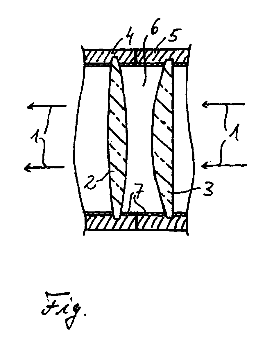
Applications Claiming Priority (2)
| Application Number | Priority Date | Filing Date | Title |
|---|---|---|---|
| DE10109031 | 2001-02-24 | ||
| DE2001109031 DE10109031A1 (de) | 2001-02-24 | 2001-02-24 | Optisches Strahlführungssystem und Verfahren zur Kontaminationsverhinderung optischer Komponenten hiervon |
Publications (2)
| Publication Number | Publication Date |
|---|---|
| EP1235110A2 EP1235110A2 (de) | 2002-08-28 |
| EP1235110A3 true EP1235110A3 (de) | 2004-02-18 |
Family
ID=7675413
Family Applications (1)
| Application Number | Title | Priority Date | Filing Date |
|---|---|---|---|
| EP20020000932 Withdrawn EP1235110A3 (de) | 2001-02-24 | 2002-01-16 | Optisches Strahlführungssystem und Verfahren zur Kontaminationsverhinderung optischer Komponenten hiervon |
Country Status (4)
| Country | Link |
|---|---|
| US (1) | US6824277B2 (de) |
| EP (1) | EP1235110A3 (de) |
| JP (1) | JP2002270502A (de) |
| DE (1) | DE10109031A1 (de) |
Families Citing this family (8)
| Publication number | Priority date | Publication date | Assignee | Title |
|---|---|---|---|---|
| DE10030495A1 (de) | 2000-06-21 | 2002-01-03 | Zeiss Carl | Verfahren zum Verbinden einer Vielzahl von optischen Elementen mit einem Grundkörper |
| JP4689058B2 (ja) * | 2001-02-16 | 2011-05-25 | キヤノン株式会社 | リニアモータ、ステージ装置および露光装置ならびにデバイス製造方法 |
| SG115621A1 (en) * | 2003-02-24 | 2005-10-28 | Asml Netherlands Bv | Method and device for measuring contamination of a surface of a component of a lithographic apparatus |
| EP1452851A1 (de) * | 2003-02-24 | 2004-09-01 | ASML Netherlands B.V. | Verfahren und Vorrichtung zur Messung der Oberflächenkontamination eines Teils eines Lithographischen Apparatus |
| EP1475668A1 (de) * | 2003-05-09 | 2004-11-10 | ASML Netherlands B.V. | Verfahren zur Herstellung von Komponenten für einen lithographischen Apparat |
| JP4386807B2 (ja) * | 2004-07-29 | 2009-12-16 | 富士通コンポーネント株式会社 | 触覚パネル |
| CA2755661C (en) * | 2009-03-27 | 2017-09-26 | Dh Technologies Development Pte. Ltd. | Heated time of flight source |
| CN109116682A (zh) * | 2017-06-23 | 2019-01-01 | 中国科学院长春光学精密机械与物理研究所 | 一种用于调整光学元件位姿的装置及调整方法 |
Citations (3)
| Publication number | Priority date | Publication date | Assignee | Title |
|---|---|---|---|---|
| US5508528A (en) * | 1993-12-03 | 1996-04-16 | Asm Lithography B.V. | Illumination unit having a facility for preventing contamination of optical components, and photolithographic apparatus including such an illumination unit |
| JPH1114876A (ja) * | 1997-06-19 | 1999-01-22 | Nikon Corp | 光学構造体、その光学構造体を組み込んだ投影露光用光学系及び投影露光装置 |
| JP2000315645A (ja) * | 1999-04-30 | 2000-11-14 | Nikon Corp | 光学部材およびその製造方法、光学装置およびこれを用いた露光装置 |
Family Cites Families (24)
| Publication number | Priority date | Publication date | Assignee | Title |
|---|---|---|---|---|
| US3969151A (en) * | 1974-01-25 | 1976-07-13 | Varian Associates | Treatment of stainless steel and similar alloys to reduce hydrogen outgassing |
| US3904277A (en) * | 1974-03-20 | 1975-09-09 | Pitney Bowes Inc | Optical hand scanner optical assembly |
| US4111762A (en) * | 1975-01-31 | 1978-09-05 | Martin Marietta Corporation | Optically black coating and process for forming it |
| DE3534366A1 (de) * | 1985-09-26 | 1987-04-02 | Siemens Ag | Verfahren zur unloesbaren befestigung von optischen elementen in einem metallischen traeger sowie haltevorrichtung fuer kugellinsen oder lichtwellenleiter |
| JPH01114876A (ja) | 1987-10-28 | 1989-05-08 | Canon Inc | 画像形成装置 |
| US5906688A (en) * | 1989-01-11 | 1999-05-25 | Ohmi; Tadahiro | Method of forming a passivation film |
| JPH01221750A (ja) * | 1988-02-29 | 1989-09-05 | Hoya Corp | パターン形成又は修正方法 |
| JPH0222612A (ja) | 1988-07-11 | 1990-01-25 | Fujitsu Ltd | レンズアセンブリ |
| US5137767A (en) * | 1990-08-29 | 1992-08-11 | Kyocera America, Inc. | Partially coated assembly structure and method for making a ceramic lid for hermetic sealing of an eprom circuit |
| JP3218802B2 (ja) * | 1993-05-07 | 2001-10-15 | 株式会社神戸製鋼所 | 半導体製造装置用ステンレス鋼材の表面処理法 |
| US5696623A (en) * | 1993-08-05 | 1997-12-09 | Fujitsu Limited | UV exposure with elongated service lifetime |
| BE1007907A3 (nl) * | 1993-12-24 | 1995-11-14 | Asm Lithography Bv | Lenzenstelsel met in gasgevulde houder aangebrachte lenselementen en fotolithografisch apparaat voorzien van een dergelijk stelsel. |
| US5685895A (en) * | 1994-08-10 | 1997-11-11 | Nikon Corporation | Air cleaning apparatus used for an exposure apparatus |
| JPH10340748A (ja) * | 1997-06-06 | 1998-12-22 | Hitachi Chem Co Ltd | 回路電極の接続方法 |
| US6014263A (en) * | 1998-05-04 | 2000-01-11 | General Electric Company | Optical lens and method of preventing clouding thereof at high temperatures |
| DE19830438A1 (de) * | 1998-07-08 | 2000-01-13 | Zeiss Carl Fa | Verfahren zur Dekontamination von Mikrolithographie-Projektionsbelichtungsanlagen |
| WO2000042639A1 (en) * | 1999-01-13 | 2000-07-20 | Nikon Corporation | Method and apparatus for projection exposure |
| US6520650B2 (en) * | 1999-02-08 | 2003-02-18 | Valeo Sylvania L.C.C. | Lamp reflector with a barrier coating of a plasma polymer |
| JP2000277413A (ja) * | 1999-03-24 | 2000-10-06 | Canon Inc | 露光量制御方法、露光装置およびデバイス製造方法 |
| JP2001110710A (ja) * | 1999-10-08 | 2001-04-20 | Nikon Corp | 露光装置、露光方法、および半導体デバイスの製造方法 |
| KR100345320B1 (ko) * | 1999-12-23 | 2002-07-24 | 학교법인 포항공과대학교 | 스테인레스 스틸 표면상에 크롬산화막을 형성하는 방법 |
| JP2001345263A (ja) * | 2000-03-31 | 2001-12-14 | Nikon Corp | 露光装置及び露光方法、並びにデバイス製造方法 |
| US6496248B2 (en) * | 2000-12-15 | 2002-12-17 | Nikon Corporation | Stage device and exposure apparatus and method |
| US6555234B1 (en) * | 2001-02-01 | 2003-04-29 | Advanced Micro Devices, Inc. | Barrier for and a method of reducing outgassing from a photoresist material |
-
2001
- 2001-02-24 DE DE2001109031 patent/DE10109031A1/de not_active Withdrawn
-
2002
- 2002-01-16 EP EP20020000932 patent/EP1235110A3/de not_active Withdrawn
- 2002-02-06 JP JP2002028953A patent/JP2002270502A/ja active Pending
- 2002-02-22 US US10/079,580 patent/US6824277B2/en not_active Expired - Lifetime
Patent Citations (3)
| Publication number | Priority date | Publication date | Assignee | Title |
|---|---|---|---|---|
| US5508528A (en) * | 1993-12-03 | 1996-04-16 | Asm Lithography B.V. | Illumination unit having a facility for preventing contamination of optical components, and photolithographic apparatus including such an illumination unit |
| JPH1114876A (ja) * | 1997-06-19 | 1999-01-22 | Nikon Corp | 光学構造体、その光学構造体を組み込んだ投影露光用光学系及び投影露光装置 |
| JP2000315645A (ja) * | 1999-04-30 | 2000-11-14 | Nikon Corp | 光学部材およびその製造方法、光学装置およびこれを用いた露光装置 |
Non-Patent Citations (2)
| Title |
|---|
| PATENT ABSTRACTS OF JAPAN vol. 1999, no. 04 30 April 1999 (1999-04-30) * |
| PATENT ABSTRACTS OF JAPAN vol. 2000, no. 14 5 March 2001 (2001-03-05) * |
Also Published As
| Publication number | Publication date |
|---|---|
| EP1235110A2 (de) | 2002-08-28 |
| US20020145808A1 (en) | 2002-10-10 |
| JP2002270502A (ja) | 2002-09-20 |
| US6824277B2 (en) | 2004-11-30 |
| DE10109031A1 (de) | 2002-09-05 |
Similar Documents
| Publication | Publication Date | Title |
|---|---|---|
| ATE327211T1 (de) | Verfahren zur uv-aushärtung einer beschichteten faser | |
| EP1235110A3 (de) | Optisches Strahlführungssystem und Verfahren zur Kontaminationsverhinderung optischer Komponenten hiervon | |
| ATE505239T1 (de) | Flammenhemmendes system und verfahren zur durchführung mindestens eines kabels, rohres oder dergleichen durch eine öffnung in einer wand | |
| DE69636282D1 (de) | Verfahren zur zuteilung der stockwerkrufe bei einer aufzugsgruppe | |
| EP0987801A3 (de) | Verfahren zur Herstellung eines optoelektronischen Bauelements | |
| EP1282011A3 (de) | Reflektives Projektionsobjektiv für EUV-Photolithographie | |
| EP0874283A3 (de) | Optischer Belichtungsapparat und optisches Reinigungsverfahren | |
| EP1128219A3 (de) | Belichtungsverfahren und -apparat | |
| ATE553402T1 (de) | Filmbeschichtete optische lithographieelemente und verfahren zur herstellung | |
| DE69832106D1 (de) | Optische Übertragungsröhre, Verfahren zu deren Herstellung und lineares Beleuchtungssystem | |
| TW200519410A (en) | Light beam converter, optical illuminating apparatus, exposure device, and exposure method | |
| DE50308894D1 (de) | Verfahren zur einstellung einer gewünschten optischen eigenschaft eines projektionsobjektivs sowie mikrolithografische projektionsbelichtungsanlage | |
| EP1906225A3 (de) | Miniaturisiertes optisch abbildendes System mit hoher lateraler und axialer Auflösung | |
| EP1258780A3 (de) | Optisches Abbildungssystem mit Polarisationsmitteln und Quarzkristallplatte hierfür | |
| DE60208628D1 (de) | Verfahren zur Herstellung optischer Lichtwellenleiter aus einer Silsesquioxanzusammensetzung | |
| EP0895113A2 (de) | Optik-Fassung mit UV-Kleber und Schutzschicht | |
| DE60236637D1 (de) | Belichtungsapparat, Belichtungsverfahren, Verwendung eines solchen Belichtungsapparats und Verfahren zur Herstellung von Vorrichtungen | |
| EP1586949A3 (de) | Belichtungsapparat und Belichtungsverfahren unter Verwendung von EUV-Licht | |
| DE60304066D1 (de) | Verfahren zur Normalisierung einer Diskursrepräsentationsstruktur und normalisierte Datenstruktur | |
| EP1202100A3 (de) | Beleuchtungssystem mit reduzierter Wärmebelastung | |
| DE102017216458A1 (de) | Verfahren zur Herstellung eines Spiegels als optischer Komponente für ein optisches System einer Projektionsbelichtungsanlage für die Projektionslithographie | |
| EP1117001A3 (de) | Lithographieverfahren und Maske zu dessen Durchführung | |
| DE69512354D1 (de) | Verfahren zur optischen Projektionsbelichtung | |
| TW200715372A (en) | Exposure method | |
| EP1666948A3 (de) | Verfahren zur Steuerung der Betriebsarten eines Stereo-Operationsmikroskops |
Legal Events
| Date | Code | Title | Description |
|---|---|---|---|
| PUAI | Public reference made under article 153(3) epc to a published international application that has entered the european phase |
Free format text: ORIGINAL CODE: 0009012 |
|
| AK | Designated contracting states |
Kind code of ref document: A2 Designated state(s): AT BE CH CY DE DK ES FI FR GB GR IE IT LI LU MC NL PT SE TR |
|
| AX | Request for extension of the european patent |
Free format text: AL;LT;LV;MK;RO;SI |
|
| PUAL | Search report despatched |
Free format text: ORIGINAL CODE: 0009013 |
|
| AK | Designated contracting states |
Kind code of ref document: A3 Designated state(s): AT BE CH CY DE DK ES FI FR GB GR IE IT LI LU MC NL PT SE TR |
|
| AX | Request for extension of the european patent |
Extension state: AL LT LV MK RO SI |
|
| 17P | Request for examination filed |
Effective date: 20040429 |
|
| 17Q | First examination report despatched |
Effective date: 20040625 |
|
| RAP1 | Party data changed (applicant data changed or rights of an application transferred) |
Owner name: CARL ZEISS SMT AG |
|
| AKX | Designation fees paid |
Designated state(s): DE FR GB NL |
|
| RAP1 | Party data changed (applicant data changed or rights of an application transferred) |
Owner name: CARL ZEISS SMT AG |
|
| RAP1 | Party data changed (applicant data changed or rights of an application transferred) |
Owner name: CARL ZEISS SMT GMBH |
|
| STAA | Information on the status of an ep patent application or granted ep patent |
Free format text: STATUS: THE APPLICATION IS DEEMED TO BE WITHDRAWN |
|
| 18D | Application deemed to be withdrawn |
Effective date: 20120306 |