EP1235200A2 - Anordnung zur Ansteuerung von Anzeigeeinheiten mit adaptiver Startsequenz - Google Patents
Anordnung zur Ansteuerung von Anzeigeeinheiten mit adaptiver Startsequenz Download PDFInfo
- Publication number
- EP1235200A2 EP1235200A2 EP02100176A EP02100176A EP1235200A2 EP 1235200 A2 EP1235200 A2 EP 1235200A2 EP 02100176 A EP02100176 A EP 02100176A EP 02100176 A EP02100176 A EP 02100176A EP 1235200 A2 EP1235200 A2 EP 1235200A2
- Authority
- EP
- European Patent Office
- Prior art keywords
- voltage
- voltage multiplier
- multiplier
- partial
- unit
- Prior art date
- Legal status (The legal status is an assumption and is not a legal conclusion. Google has not performed a legal analysis and makes no representation as to the accuracy of the status listed.)
- Withdrawn
Links
Images


Classifications
-
- G—PHYSICS
- G09—EDUCATION; CRYPTOGRAPHY; DISPLAY; ADVERTISING; SEALS
- G09G—ARRANGEMENTS OR CIRCUITS FOR CONTROL OF INDICATING DEVICES USING STATIC MEANS TO PRESENT VARIABLE INFORMATION
- G09G3/00—Control arrangements or circuits, of interest only in connection with visual indicators other than cathode-ray tubes
- G09G3/20—Control arrangements or circuits, of interest only in connection with visual indicators other than cathode-ray tubes for presentation of an assembly of a number of characters, e.g. a page, by composing the assembly by combination of individual elements arranged in a matrix no fixed position being assigned to or needed to be assigned to the individual characters or partial characters
- G09G3/34—Control arrangements or circuits, of interest only in connection with visual indicators other than cathode-ray tubes for presentation of an assembly of a number of characters, e.g. a page, by composing the assembly by combination of individual elements arranged in a matrix no fixed position being assigned to or needed to be assigned to the individual characters or partial characters by control of light from an independent source
- G09G3/36—Control arrangements or circuits, of interest only in connection with visual indicators other than cathode-ray tubes for presentation of an assembly of a number of characters, e.g. a page, by composing the assembly by combination of individual elements arranged in a matrix no fixed position being assigned to or needed to be assigned to the individual characters or partial characters by control of light from an independent source using liquid crystals
-
- H—ELECTRICITY
- H02—GENERATION; CONVERSION OR DISTRIBUTION OF ELECTRIC POWER
- H02M—APPARATUS FOR CONVERSION BETWEEN AC AND AC, BETWEEN AC AND DC, OR BETWEEN DC AND DC, AND FOR USE WITH MAINS OR SIMILAR POWER SUPPLY SYSTEMS; CONVERSION OF DC OR AC INPUT POWER INTO SURGE OUTPUT POWER; CONTROL OR REGULATION THEREOF
- H02M3/00—Conversion of DC power input into DC power output
- H02M3/02—Conversion of DC power input into DC power output without intermediate conversion into AC
- H02M3/04—Conversion of DC power input into DC power output without intermediate conversion into AC by static converters
- H02M3/06—Conversion of DC power input into DC power output without intermediate conversion into AC by static converters using resistors or capacitors, e.g. potential divider
- H02M3/07—Conversion of DC power input into DC power output without intermediate conversion into AC by static converters using resistors or capacitors, e.g. potential divider using capacitors charged and discharged alternately by semiconductor devices with control electrode, e.g. charge pumps
-
- G—PHYSICS
- G09—EDUCATION; CRYPTOGRAPHY; DISPLAY; ADVERTISING; SEALS
- G09G—ARRANGEMENTS OR CIRCUITS FOR CONTROL OF INDICATING DEVICES USING STATIC MEANS TO PRESENT VARIABLE INFORMATION
- G09G3/00—Control arrangements or circuits, of interest only in connection with visual indicators other than cathode-ray tubes
- G09G3/20—Control arrangements or circuits, of interest only in connection with visual indicators other than cathode-ray tubes for presentation of an assembly of a number of characters, e.g. a page, by composing the assembly by combination of individual elements arranged in a matrix no fixed position being assigned to or needed to be assigned to the individual characters or partial characters
- G09G3/34—Control arrangements or circuits, of interest only in connection with visual indicators other than cathode-ray tubes for presentation of an assembly of a number of characters, e.g. a page, by composing the assembly by combination of individual elements arranged in a matrix no fixed position being assigned to or needed to be assigned to the individual characters or partial characters by control of light from an independent source
- G09G3/36—Control arrangements or circuits, of interest only in connection with visual indicators other than cathode-ray tubes for presentation of an assembly of a number of characters, e.g. a page, by composing the assembly by combination of individual elements arranged in a matrix no fixed position being assigned to or needed to be assigned to the individual characters or partial characters by control of light from an independent source using liquid crystals
- G09G3/3611—Control of matrices with row and column drivers
-
- G—PHYSICS
- G09—EDUCATION; CRYPTOGRAPHY; DISPLAY; ADVERTISING; SEALS
- G09G—ARRANGEMENTS OR CIRCUITS FOR CONTROL OF INDICATING DEVICES USING STATIC MEANS TO PRESENT VARIABLE INFORMATION
- G09G2330/00—Aspects of power supply; Aspects of display protection and defect management
- G09G2330/02—Details of power systems and of start or stop of display operation
- G09G2330/026—Arrangements or methods related to booting a display
-
- G—PHYSICS
- G09—EDUCATION; CRYPTOGRAPHY; DISPLAY; ADVERTISING; SEALS
- G09G—ARRANGEMENTS OR CIRCUITS FOR CONTROL OF INDICATING DEVICES USING STATIC MEANS TO PRESENT VARIABLE INFORMATION
- G09G3/00—Control arrangements or circuits, of interest only in connection with visual indicators other than cathode-ray tubes
- G09G3/20—Control arrangements or circuits, of interest only in connection with visual indicators other than cathode-ray tubes for presentation of an assembly of a number of characters, e.g. a page, by composing the assembly by combination of individual elements arranged in a matrix no fixed position being assigned to or needed to be assigned to the individual characters or partial characters
- G09G3/34—Control arrangements or circuits, of interest only in connection with visual indicators other than cathode-ray tubes for presentation of an assembly of a number of characters, e.g. a page, by composing the assembly by combination of individual elements arranged in a matrix no fixed position being assigned to or needed to be assigned to the individual characters or partial characters by control of light from an independent source
- G09G3/36—Control arrangements or circuits, of interest only in connection with visual indicators other than cathode-ray tubes for presentation of an assembly of a number of characters, e.g. a page, by composing the assembly by combination of individual elements arranged in a matrix no fixed position being assigned to or needed to be assigned to the individual characters or partial characters by control of light from an independent source using liquid crystals
- G09G3/3611—Control of matrices with row and column drivers
- G09G3/3696—Generation of voltages supplied to electrode drivers
Definitions
- the invention relates to a circuit arrangement with a partial voltage generation unit and a voltage multiplier for generating at least one voltage. Furthermore, the invention relates to a voltage multiplier and an arrangement for Control of a display device and a display device with such Arrangement and an electronic device with a display unit for displaying Image data with an arrangement for controlling this display unit.
- Voltage multipliers are required in devices that have a higher voltage is required than the available supply voltage. In particular these become voltage multipliers for driver circuits for display devices used. In order to drive modern liquid crystal displays, it is necessary to use voltages Provide the supply voltage to the driver circuit by one Exceed many times. Voltage multiplier circuits are usually called Charge pumps run with the available system supply voltage are operated, the system supply voltage through the series circuit of pump stages, which in principle each consist of a switch or a diode and a capacitor exist, is pumped up to the required output voltage.
- the display technology will play an increasingly important role in the next few years Information and communication technology too.
- the display device As an interface between people and In the digital world, the display device is of central importance for acceptance modern information systems.
- portable devices such as notebooks, Phones, digital cameras and personal digital assistants are without the use of Displays cannot be realized.
- driver circuits or arrangements for driving these display devices used For the control of such display devices or Displays become driver circuits or arrangements for driving these display devices used. These driver circuits convert the image signals onto one Display should be shown.
- the image information is stored in storage media as digital signals stored. These digital signals must be converted into analog signals be converted so that a corresponding one by means of an analog voltage Contrast can be achieved on the display.
- the above display devices are mainly used in battery operated Devices used, so that low power consumption and corresponding power efficiency become more and more important. Furthermore, the space required in such Equipment is playing a critical role, so any space savings and Weight loss brings a crucial benefit. Not or only for a short time The required components or components are additional electricity consumers that too Show a corresponding power consumption during their inactive time.
- DE 19639701 specifies a control circuit for voltage multipliers which monitors the output voltage. A dependent on the output voltage The control signal is fed to the drivers of a charge pump via a comparator. This turns the charge pump on or off depending on the output voltage allows. Undefined states at the start of this circuit can malfunction of the circuit. The unsafe conditions do not work defined voltages in the initial state of the charge pump and its control circuit back. For example, the partial voltage generation can be undefined and the Partial voltage, which is compared with a reference voltage supplied from outside, be greater than the reference voltage, whereby the charge pump is not started, so that the output voltage of the charge pump cannot rise, which ultimately increases malfunction of the overall arrangement.
- the voltage value at the output of the charge pump is zero volts or is undefined, so that the individual partial voltage values are also undefined and the charge pump may be that due to the comparison in the comparator Gets signal that no voltage multiplication is necessary.
- the object of the invention is therefore to provide a circuit arrangement which is automatic and safe starting sequence with low power consumption and takes up little space on a circuit.
- This object is achieved with a circuit arrangement for generating at least one voltage value solved that a partial voltage generation unit and a voltage multiplier contains, provided for controlling the voltage multiplier in a start time (ts) is to switch the voltage multiplier into a direct mode.
- the arrangement according to the invention is for providing an increased voltage Vmult and dependent on it several different partial voltage values. These voltage values are required, for example, to control a display must have a high accuracy in the corresponding voltage value.
- a voltage multiplier is used. This voltage multiplier is programmable in its multiplication factor, For example, by not activating all the existing stages of the voltage multiplier. Due to the programmability of the voltage multiplier, there are only ever so many Levels of the voltage multiplier operated as necessary for the respective application are. Thus, the voltage multiplier with regard to the power consumption is in each case the Application adaptable. With which multiplication factor the voltage multiplier is operated depends on the required partial voltage values, which are determined by the Supply voltage, display properties and image information to be displayed be determined.
- Displays can be operated in different operating modes, for example in differentiate the resolution. For low resolutions there are lower partial voltage values required as if the display is operated at its maximum resolution.
- the multiplication factor of the voltage multiplier can be programmed advantageous.
- an activation signal is provided to the voltage multiplier and supply an initial start signal.
- the initial start signal is in a Start time supplied to the voltage multiplier and switches it into a direct mode.
- the supply voltage Vdd is directly on the output of the voltage multiplier switched through so that there is a defined output voltage of the voltage multiplier and defined partial voltage values in the partial voltage generation unit can adjust.
- the activation signal is made from a Partial voltage and a reference signal are formed.
- the partial tension is in the Partial voltage generation unit generated, the reference signal is supplied from the outside.
- the initial start signal is generated by monitoring the activation signal. Doing so the voltage multiplier fed the initial start signal until the Activation signal has a safe logic state.
- the start start signal and the activation signal are in a start control unit generated. This is for the control of the voltage multiplier in the start time and in normal or regular operation. After being at the output of the voltage multiplier, which is operated in direct mode, a defined output voltage has defined, also set partial voltage values, so that the start control unit generates a defined activation signal and the voltage multiplier in its can change regular operation.
- the voltage multiplier is controlled by the activation signal.
- the activation signal controls whether the voltage multiplier for multiplying Tension is required or not.
- the circuit arrangement according to the invention contains a voltage multiplier and a partial voltage generating unit, wherein the partial voltage generating unit generated partial voltage values from the voltage generated by the voltage multiplier Vmult can be derived.
- the voltage multiplier On or off or in influencing its multiplication factor becomes a definable partial voltage value of derived from the partial voltage generation unit and fed to a start control unit.
- the Partial voltage value that can be determined is converted into a partial voltage generating unit associated switching unit connected to the start control unit.
- the switching unit preferably implemented as a transistor array, so that depending on the application, each available Partial voltage of the start control unit can be supplied.
- the start control unit advantageously has at least one comparator, which is implemented, for example, by a differential amplifier.
- a partial voltage value from the partial voltage generation unit is fed to this comparator.
- a reference voltage Vref applied from the outside is applied to the comparator as a comparison signal.
- the comparison of these two values leads to an activation signal.
- an initial control signal is generated in the start control unit, which is fed to the voltage multiplier.
- the activation signal is fed to a logic circuit which generates a self-adjusting start sequence which is fed to the voltage multiplier in the form of the start signal. To ensure that the time during which the voltage multiplier is operated in direct mode is as short as possible, it is necessary to observe the activation signal from the comparator.
- This condition monitoring of the activation signal makes it possible to keep the time for the initial start sequence as short as possible.
- the arrangement for controlling display units can be adapted to many different applications.
- this condition monitoring enables a safe and quick start of the arrangement, and, in addition, complex additional circuit components to ensure a safe start are not required.
- the reference signal that is fed to the comparator can be a temperature function, for example describe. Since display units are temperature dependent, among other things voltage values may be necessary at lower temperatures adjust this temperature.
- the start time is the voltage multiplier in which direct mode is operated, adaptively adjustable. This will ensures that the time in which the voltage multiplier is operated in direct mode is always as short as possible.
- the voltage multiplier is in the To operate direct mode, i.e. the available supply voltage Vdd is switched directly to the output of the voltage multiplier, without the steps the charge pump can be activated.
- the partial voltage generation unit connected to the output voltage Vmult provided by the voltage multiplier be, i.e. the partial voltage generation unit becomes the supply voltage in the start time Vdd supplied.
- the reference voltage Vref is fed to the comparator, however, the reference voltage Vref with the lowest temperature coefficient should be here can be selected to be as temperature-independent as possible during this time.
- the control voltages Vop for the switching unit for generating the Partial voltage value for supply to the comparator to the maximum possible voltage be switched.
- the maximum possible voltage is Supply voltage Vdd available
- the control voltages Vop for controlling the switching unit are determined by the output voltage derived from the voltage multiplier and voltage values between Take mass or Vss and Vmult.
- the partial voltage that is fed to the comparator depends on the available partial voltage values of the voltage divider - the The highest voltage can be at most Vdd in the start time.
- a low load at the output of the device is advantageous for a quick start of the arrangement Charge pump, causing capacities of the assembly to be loaded as quickly as possible can be. So if the height of the load is adjustable, it should be as low as This is possible, for example, by having all connected to the circuit arrangement connected driver circuits, for example for controlling a display unit, be switched off.
- the charge pump is provided in to switch the direct mode.
- the supply voltage Vdd is directly on the Output of the voltage multiplier or the charge pump switched through.
- a Charge pump consists of a series connection of several pump stages, each pump stage has at least one switch or a diode and a charge storage element. The switches are opened and closed after a periodic signal. To the charge storage elements are correspondingly charged by means of driver circuits. The charge present in each stage is thus passed on from stage to stage.
- the charge storage elements represent a capacitive load that must be charged before the supply voltage at the output of the voltage multiplier is applied.
- the charge pump can connect have, which bridges the stages of the charge pump in direct mode and thus one direct connection from the input of the voltage multiplier to its output realized.
- the voltage multiplier starts is a test to be carried out during the manufacture of a such a circuit less expensive, since, for example, only one comparator has been tested must become.
- Such an arrangement can be further developed in that a further comparator a different partial voltage value with a reference voltage is introduced compares so that the two partial voltage values fed to the two comparators will have a different voltage in each case, so that when switched on the charge pump can be started safely.
- the task is also generated by a voltage multiplier at least a voltage value with a series connection of stages with switching devices, Switching devices and capacities solved, during which the switching devices during a start time are closed and therefore at the input of the voltage multiplier applied supply voltage is switched through to the output of the voltage multiplier is and the capacities can be switched off by means of the switching devices.
- This starting procedure also known as direct mode, becomes faster Voltage value reached.
- the direct mode can be used with voltage multipliers fixed multiplication, as well as with voltage multipliers with programmable Multiplication can be used.
- the object is also achieved by a circuit arrangement for controlling a display device with a partial voltage generator unit and a voltage multiplier solved, which is provided for controlling the voltage multiplier, the voltage multiplier by means of an initial start signal in a start time (ts) in a direct mode to switch.
- the partial voltage generation unit to provide different partial voltage values at the same time Control of the lines of a display and to provide a partial voltage value used to control the voltage multiplier.
- the task is also performed by a display unit for displaying image data with a Arrangement for controlling the display unit with a partial voltage generator unit and solved a voltage multiplier, which is provided, the voltage multiplier to switch to a direct mode by means of at least one signal in a start time.
- the task is also performed by an electronic device with a display unit for display of image data and with an arrangement for controlling the display unit with solved a partial voltage generator unit and a voltage multiplier, in which at least one signal is provided for controlling the voltage multiplier and the Voltage multiplier can be switched to a direct mode in a start time (ts).
- the task is also accomplished using a method for starting a circuit arrangement solved a partial voltage generator unit and a voltage multiplier, in which by comparing a partial voltage value and a reference voltage Activation signal is generated and in which the voltage multiplier during a Start time (ts) is switched to a direct mode and the start time (ts) by monitoring an activation signal is adjusted adaptively.
- An arrangement 15 for controlling the display unit contains a voltage multiplier 20, a partial voltage generation unit 40 and a start control unit 30.
- the supply voltage Vdd 21 is supplied to the voltage multiplier 20.
- the Voltage multiplier 20 generates from this supply voltage 21 by means of several Pump stages a higher voltage Vmult 22.
- the start control unit 30 is provided.
- the start control unit 30 contains a comparator 31 and a logic unit 35.
- the start control unit 30 becomes a partial voltage value Vdac 34 and a reference voltage Vref 33 are supplied. This reference voltage is generated in a bandgap circuit.
- a bandgap circuit is a circuit with which a voltage can be generated the value of which is given by semiconductor physics. Such circuits are used for Generation of reference voltages used. The voltage generated is different from that used Semiconductor material (Si, Ge, GaAs, InPh, etc.) hardly determines and varies in mass production. This can also result in a targeted temperature dependence of the generated Voltage can be realized.
- Semiconductor material Si, Ge, GaAs, InPh, etc.
- the comparator 31 compares these supplied voltage values 31 and 34 before and generates the activation signal 32.
- the activation signal 32 is the Voltage multiplier 20 and the logic unit 35 supplied.
- the logic unit 35 generates the start signal 36.
- the logic unit 35 is also capable of power supply for the voltage multiplier 20. off.
- Vmult 22 generated by the voltage multiplier 20 are over one voltage divider chain 42, which is implemented, for example, as a resistance chain, several Partial voltage values Vpart generated.
- the switching device 41 which, for example, as Transistor array is realized, one of the partial voltages Vteil becomes the start control unit 30 passed as signal 34.
- the different partial voltage values Vteil are both the Switching device 41, as well as via the connections A1-An shown in Figure 3
- Amplifier circuit 10 for driving the lines Z of a display 2 is supplied.
- the Switching control device 41 is by means of a transistor array 41 shown in more detail in FIG realized and is controlled via voltages Vop. These voltages are from Vop the voltage Vmult 22 derived.
- Vop can have the following voltage values: either Mass (Vss) or Vmult.
- Vmult is determined by the regulation, but can be a maximum M * Vdd, where M is the selected multiplication factor of the voltage multiplier.
- the activation signal 32 as a result of the comparator 31 is sent by the logic unit 35 supervised. In this logic unit 35, the self-adjusting start sequence is used for generation of the start signal 36 is generated.
- the voltage multiplier becomes in the start time ts 20 operated in a direct mode.
- the supply voltage Vdd 21 connected directly to the output of the voltage multiplier 20, so that the Output voltage 22 Vmult of the voltage multiplier 20 of the supply voltage Vdd 21 corresponds.
- FIG. 2 shows a diagram in which the course of the start signal 36 is shown is.
- the initial start signal 36 is generated by the logic unit 35.
- Start time ts which is composed of a portion of a fixed time tf, a monitoring time tc and a delay time td, the initial start signal 36 to the Voltage multiplier directed.
- the activation signal 32 is checked or monitored by the logic unit. If the activation signal 32 changes to logic state 1 or during this time tc remains in this state and an additional delay time td has elapsed, the Voltage multiplier 20 switched from direct mode to normal operation.
- the voltage multiplier From this moment on, the activation signal 32 controls 20.
- the time tf and also the time td can also be 0, depending on the application. Thereby the time in which the voltage multiplier is operated in direct mode can be very short being held.
- the driver circuit 1 contains a memory 9 in which the image data are stored Furthermore, the driver circuit 1 contains an arrangement 15 for controlling a Display unit.
- a switching and amplifier device 10 carries out the arrangement 15 generated partial voltages to a switch 7.
- a function generator 6 generates sets of orthogonal functions. These sets of orthogonal functions are used on the Switch 7 led. There are the provided partial voltages and the orthogonal Functions linked and brought up to the respective lines Z of the display 2.
- the generated partial voltage values and the supply voltages Vmult, Vdd and Vss are also fed to the switch 8.
- the switch 8 is also the orthogonal Functions of the function generator 6 provided. In the switch 8 is the set of the orthogonal functions and the image data read out from the memory 9 calculated a column tension. This column tension is then from the set of Available partial voltages are selected and sent to columns S of display 2 created.
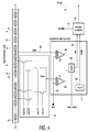
- FIG. 4 shows an arrangement for controlling, for example, a display device an additional start comparator 37.
- This arrangement contains, like FIG a resistor chain 42 for generating partial voltage values, a voltage multiplier 20, a start control unit 30, a switching device designed as a transistor array 41, a logic block 48, a comparator 31 and a further logic block 38.
- a partial voltage value 39 is supplied to the start comparator 37.
- This start comparator 37 generates an output signal 44 which is supplied to logic block 38.
- the comparison signal 43 of the comparator 31 is also supplied to the logic block 38.
- This logic block 38 is ORed, which in turn is a Activation signal 32 leads to voltage multiplier 20.
- the contains two comparators 31 and 37 it is possible to generate a start signal which enables safe starting of the voltage multiplier 20.
- the start control unit 30 generates a safe activation signal 32.
- the control signals Vop are derived from Vmult. Vop can voltage values between Vss (mass) and Vmult. For low voltage values of Vmult (startup) Vdac 34 is not defined. Only when the voltage Vmult high enough Vdac is defined and the comparator 31 can use the signal 43 to control the Take over voltage multiplier 20.
- the relationship between signal 39 and voltage 29 Vmult is selected such that the start comparator 37 has at least the voltage multiplier 20 activated until Vmult is high enough to define Vdac.
- the function of the logic unit 48 in FIG. 4 is different from that of the logic unit 35 in FIG. 1. In the Logic unit 48 becomes, for example, the multiplication factor M of the voltage multiplier 20 set. Logic unit 48 is also capable of power supply for the voltage multiplier 20 on or off.
- FIG. 5 shows an arrangement of a voltage multiplier with devices for the Direct fashion shown.
- the voltage multiplier 20 is shown in a very simplified manner. He contains several stages S1 to Sn, each a switching device SWn, a switching device SCn and a capacitor CSn included.
- the supply voltage Vdd switched directly to the Vmult output.
- the switching devices SWn closed. It is advantageous to keep the capacitive load low to switch off the capacitors of the stages from direct connection Vdd to Vmult.
- the switching devices SCn are provided for this purpose. These are in direct mode open. In normal mode, these switching devices SCn are closed or conductive.
- a direct connection is provided between the input Vdd of the voltage multiplier and the output Vmult turn.
- at least one switching device SA1 is provided, which if necessary can be supplemented by a further switching device SA2.
- the embodiment to choose is application-dependent, the space available on the circuit and the respective additional power consumption must be taken into account.
- An arrangement 15 according to the invention can also be used for the power supply of Flashmemories or similar applications are used that have a higher voltage need than the one provided by the system supply voltage becomes.
Landscapes
- Engineering & Computer Science (AREA)
- Chemical & Material Sciences (AREA)
- Crystallography & Structural Chemistry (AREA)
- Physics & Mathematics (AREA)
- Computer Hardware Design (AREA)
- General Physics & Mathematics (AREA)
- Theoretical Computer Science (AREA)
- Power Engineering (AREA)
- Control Of Indicators Other Than Cathode Ray Tubes (AREA)
- Liquid Crystal Display Device Control (AREA)
- Dc-Dc Converters (AREA)
- Liquid Crystal (AREA)
Abstract
Description
Dadurch lässt sich die Anordnung zur Ansteuerung von Anzeigeeinheiten an viele unterschiedliche Anwendungen anpassen. Gleichzeitig wird durch diese Zustandsüberwachung ein sicherer und schneller Start der Anordnung ermöglicht, wobei außerdem aufwendige zusätzliche Schaltungskomponenten zur Sicherstellung eines sicheren Starts nicht benötigt werden.
- Fig.1
- Anordnung zur Ansteuerung einer Anzeigeeinheit ohne zusätzlichen Startkomparator
- Fig.2
- Startsequenz
- Fig.3
- Anzeigeeinheit
- Fig.4
- Anordnung zur Ansteuerung einer Anzeigeeinheit mit einem Startkomparator
- Fig 5
- Anordnung eines Spannungsvervielfachers mit Vorrichtungen für den Direktmode
Claims (10)
- Schaltungsanordnung (15) zur Erzeugung wenigstens eines Spannungswertes (Vmult) mit einer Teilspannungserzeugereinheit (40) und einem Spannungsvervielfacher (20), bei der zur Steuerung des Spannungsvervielfachers in einer Startzeit (ts) vorgesehen ist, den Spannungsvervielfacher in einen Direktmode zu schalten.
- Schaltungsanordnung nach Anspruch 1,
dadurch gekennzeichnet, dass vorgesehen ist, dem Spannungsvervielfacher ein Aktivierungssignal (32) zuzuführen, das aus einer von der Teilspannungserzeugungseinheit erzeugten Teilspannung (Vdac) und einem Referenzsignal (Vref) gebildet ist und dass vorgesehen ist, dem Spannungsvervielfacher während der Startzeit (ts) ein aus dem Aktivierungssignal (32) gebildetes Anfangsstartsignal (36) zuzuführen. - Schaltungsanordnung nach Anspruch 1,
dadurch gekennzeichnet, dass eine Startsteuereinheit zur Steuerung des Spannungsvervielfachers vorgesehen ist, die zumindest einen Vergleicher (31) und eine Logikeinheit (35) enthält, wobei der Vergleicher zum Vergleich einer von der Teilspannungserzeugungseinheit erzeugten Teilspannung (Vdac) und einer Referenzspannung (Vref) und zur Erzeugung des Aktivierungssignals (32)vorgesehen ist, und eine Logikeinheit 35 ein Anfangsstartsignal (36) erzeugt, um den Spannungsvervielfacher in einen Direktmode zu schalten. - Schaltungsanordnung nach Anspruch 1,
dadurch gekennzeichnet, dass die Startzeit (ts), in der der Spannungsvervielfacher (20) in einem Direktmode betrieben wird, adaptiv einstellbar ist. - Schaltungsanordnung nach Anspruch 1,
dadurch gekennzeichnet, dass eine Serienschaltung von Schalteinrichtungen (SWn) der Stufen (Sn) im Spannungsvervielfacher (20) im Direktmode geschlossen sind und die den Stufen zugeordneten Kapazitäten (CSn) abschaltbar sind. - Schaltungsanordnung zur Ansteuerung einer Anzeigevorrichtung mit einer Teilspannungserzeugereinheit (40) und einem Spannungsvervielfacher (20), bei der zur Steuerung des Spannungsvervielfachers (20) vorgesehen ist, den Spannungsvervielfacher mittels eines Anfangsstartsignals (36) in einer Startzeit (ts) in einen Direktmode zu schalten.
- Spannungsvervielfacher zur Erzeugung wenigstens eines Spannungswertes (Vmult) mit einer Serienschaltung von Stufen (Sn) mit Schalteinrichtungen (SWn), Schalteinrichtungen (SCn) und Kapazitäten (CSn),
dadurch gekennzeichnet dass,
während einer Startzeit (ts) die Schalteinrichtungen (SWn) geschlossen sind und dadurch am Eingang des Spannungsvervielfachers anliegende Versorgungsspannung (Vdd) auf den Ausgang des Spannungsvervielfachers durchgeschaltet ist. - Anzeigeeinheit (2) zur Darstellung von Bilddaten mit einer Anordnung (15) zur Ansteuerung der Anzeigeeinheit mit einer Teilspannungserzeugereinheit (40) und einem Spannungsvervielfacher (20), bei der vorgesehen ist, den Spannungsvervielfacher in einer Startzeit (ts) mittels wenigstens einem Signal (36) in einen Direktmode zu schalten.
- Elektronisches Gerät mit einer Anzeigeeinheit (2) zur Darstellung von Bilddaten und mit einer Anordnung (15) zur Ansteuerung der Anzeigeeinheit mit einer Teilspannungserzeugereinheit (40) und einem Spannungsvervielfacher (20), bei der wenigstens ein Signal (36) zur Steuerung des Spannungsvervielfachers vorgesehen ist und der Spannungsvervielfacher in einer Startzeit (ts) in einen Direktmode schaltbar ist.
- Verfahren zum Starten einer Schaltungsanordnung (15) mit einer Teilspannungserzeugereinheit (40), einem Spannungsvervielfacher (20), bei dem mittels eines Vergleichs eines Teilspannungswertes (Vteil) und einer Referenzspannung (Vref) ein Aktivierungssignal (32) erzeugt wird und bei dem der Spannungsvervielfacher (20) während einer Startzeit (ts) in einen Direktmode geschaltet wird und die Startzeit (ts) durch Überwachen eines Aktivierungssignals (32) adaptiv eingestellt wird.
Applications Claiming Priority (2)
| Application Number | Priority Date | Filing Date | Title |
|---|---|---|---|
| DE10108980 | 2001-02-23 | ||
| DE10108980A DE10108980A1 (de) | 2001-02-23 | 2001-02-23 | Anordnung zur Ansteuerung von Anzeigeeinheiten mit adaptiver Startsequenz |
Publications (2)
| Publication Number | Publication Date |
|---|---|
| EP1235200A2 true EP1235200A2 (de) | 2002-08-28 |
| EP1235200A3 EP1235200A3 (de) | 2009-08-05 |
Family
ID=7675383
Family Applications (1)
| Application Number | Title | Priority Date | Filing Date |
|---|---|---|---|
| EP02100176A Withdrawn EP1235200A3 (de) | 2001-02-23 | 2002-02-22 | Anordnung zur Ansteuerung von Anzeigeeinheiten mit adaptiver Startsequenz |
Country Status (6)
| Country | Link |
|---|---|
| US (1) | US6914473B2 (de) |
| EP (1) | EP1235200A3 (de) |
| JP (1) | JP4298206B2 (de) |
| KR (1) | KR100847995B1 (de) |
| CN (1) | CN1320739C (de) |
| DE (1) | DE10108980A1 (de) |
Families Citing this family (7)
| Publication number | Priority date | Publication date | Assignee | Title |
|---|---|---|---|---|
| KR100605575B1 (ko) * | 2004-06-30 | 2006-07-31 | 주식회사 하이닉스반도체 | 테스트 모드시 전하 펌프에서의 토글링 주기를 변경할 수있는 내부 전압 발생 회로 및 방법 |
| CN100382418C (zh) * | 2005-04-05 | 2008-04-16 | 矽创电子股份有限公司 | 一种可程控调整输出电压的倍增电路 |
| US7307468B1 (en) * | 2006-01-31 | 2007-12-11 | Xilinx, Inc. | Bandgap system with tunable temperature coefficient of the output voltage |
| JP4843472B2 (ja) * | 2006-03-13 | 2011-12-21 | 株式会社東芝 | 電圧発生回路 |
| KR101022106B1 (ko) * | 2008-08-06 | 2011-03-17 | 삼성모바일디스플레이주식회사 | 유기전계발광표시장치 |
| DE102009014509B4 (de) * | 2009-03-24 | 2015-05-07 | Texas Instruments Deutschland Gmbh | Elektronische Vorrichtung und Verfahren zur Ansteuerung einer Anzeige |
| DE102018218785A1 (de) * | 2018-11-05 | 2020-05-07 | Volkswagen Aktiengesellschaft | Schaltungseinheit und Verfahren zur Steuerung von Lastströmen |
Family Cites Families (22)
| Publication number | Priority date | Publication date | Assignee | Title |
|---|---|---|---|---|
| JP2831914B2 (ja) * | 1992-09-30 | 1998-12-02 | 株式会社東芝 | 半導体集積回路装置 |
| JP3267756B2 (ja) * | 1993-07-02 | 2002-03-25 | 株式会社日立製作所 | 半導体集積回路装置 |
| JP2639325B2 (ja) * | 1993-11-30 | 1997-08-13 | 日本電気株式会社 | 定電圧発生回路 |
| EP0772283B1 (de) * | 1995-10-31 | 2000-01-12 | STMicroelectronics S.r.l. | Spannungsvervielfacher mit linearen Regelung |
| US5708387A (en) * | 1995-11-17 | 1998-01-13 | Advanced Micro Devices, Inc. | Fast 3-state booster-circuit |
| US5680300A (en) * | 1995-12-22 | 1997-10-21 | Analog Devices, Inc. | Regulated charge pump DC/DC converter |
| DE19639701C2 (de) * | 1996-09-26 | 1998-12-03 | Siemens Ag | Regelschaltung für Ladungspumpen |
| AU5165798A (en) * | 1996-11-05 | 1998-05-29 | Aplus Flash Technology, Inc. | Positive/negative high voltage charge pump system |
| TW404063B (en) * | 1997-02-27 | 2000-09-01 | Toshiba Corp | Semiconductor integrated circuit apparatus and semiconductor memory apparatus |
| KR100273208B1 (ko) * | 1997-04-02 | 2000-12-15 | 김영환 | 반도체메모리장치의고효율전하펌프회로 |
| KR100264959B1 (ko) * | 1997-04-30 | 2000-10-02 | 윤종용 | 반도체 장치의 고전압발생회로 |
| JPH1166855A (ja) * | 1997-06-10 | 1999-03-09 | Fujitsu Ltd | 電位検出回路、半導体装置、及び半導体記憶装置 |
| JP3347036B2 (ja) * | 1997-10-29 | 2002-11-20 | 東芝情報システム株式会社 | アナログpll回路、半導体装置、および電圧制御発振器の発振制御方法 |
| DE19928309C2 (de) * | 1999-06-21 | 2002-03-28 | Texas Instruments Deutschland | Gleichspannungswandler |
| US6255896B1 (en) * | 1999-09-27 | 2001-07-03 | Intel Corporation | Method and apparatus for rapid initialization of charge pump circuits |
| JP2001126478A (ja) * | 1999-10-29 | 2001-05-11 | Mitsubishi Electric Corp | 半導体装置 |
| JP3372923B2 (ja) * | 2000-02-25 | 2003-02-04 | エヌイーシーマイクロシステム株式会社 | 半導体集積回路 |
| JP4149637B2 (ja) * | 2000-05-25 | 2008-09-10 | 株式会社東芝 | 半導体装置 |
| KR100383769B1 (ko) * | 2000-12-18 | 2003-05-14 | 주식회사 하이닉스반도체 | 펌핑 전압 레귤레이션 회로 |
| US6522193B2 (en) * | 2000-12-19 | 2003-02-18 | Hynix Semiconductor Inc. | Internal voltage generator for semiconductor memory device |
| US6366158B1 (en) * | 2000-12-27 | 2002-04-02 | Intel Corporation | Self initialization for charge pumps |
| JP2002208290A (ja) * | 2001-01-09 | 2002-07-26 | Mitsubishi Electric Corp | チャージポンプ回路およびこれを用いた不揮発性メモリの動作方法 |
-
2001
- 2001-02-23 DE DE10108980A patent/DE10108980A1/de not_active Ceased
-
2002
- 2002-02-19 CN CNB021077304A patent/CN1320739C/zh not_active Expired - Fee Related
- 2002-02-21 US US10/081,891 patent/US6914473B2/en not_active Expired - Fee Related
- 2002-02-21 KR KR1020020009224A patent/KR100847995B1/ko not_active Expired - Fee Related
- 2002-02-22 EP EP02100176A patent/EP1235200A3/de not_active Withdrawn
- 2002-02-25 JP JP2002047918A patent/JP4298206B2/ja not_active Expired - Fee Related
Also Published As
| Publication number | Publication date |
|---|---|
| US6914473B2 (en) | 2005-07-05 |
| CN1320739C (zh) | 2007-06-06 |
| DE10108980A1 (de) | 2002-09-12 |
| JP4298206B2 (ja) | 2009-07-15 |
| US20020130708A1 (en) | 2002-09-19 |
| KR100847995B1 (ko) | 2008-07-23 |
| JP2002372959A (ja) | 2002-12-26 |
| KR20020069136A (ko) | 2002-08-29 |
| CN1372372A (zh) | 2002-10-02 |
| EP1235200A3 (de) | 2009-08-05 |
Similar Documents
| Publication | Publication Date | Title |
|---|---|---|
| DE60315332T2 (de) | Variable ladungspumpschaltung mit dynamischer last | |
| DE60304311T2 (de) | Verbrauchsarmer Regler für eine Spannungserzeugung mittels Ladungspumpe | |
| DE69514523T2 (de) | Spannungsvervielfacher mit linearen Regelung | |
| DE602004004597T2 (de) | Spannungs-Abwärts-Wandler mit reduzierter Welligkeit | |
| DE60129969T2 (de) | Abwärtsregler mit doppelantrieb | |
| DE69711980T2 (de) | Spannungserhöhungsreglerschaltung | |
| DE102009024159A1 (de) | Elektronische Vorrichtung und Verfahren zur DC-DC-Umwandlung mit variablem Arbeitsstrom | |
| DE60023775T2 (de) | Spannungserhöhungsschaltung, Spannungserhöhungsverfahren, und elektronisches Gerät | |
| DE60204850T2 (de) | Programmierbares ladungspumpenbauelement | |
| DE102008016532A1 (de) | Dynamisch angepasster Mehrphasen-Regulator | |
| EP1980012A1 (de) | Schaltungsanordnung zur spannungsversorgung und verfahren | |
| DE10337541A1 (de) | Integrierter Schaltungsbaustein und zugehöriges Optimierungsverfahren | |
| DE102004031393A1 (de) | Gleichspannungswandler und Verfahren zur Umsetzung einer Gleichspannung | |
| DE102014119097B4 (de) | Spannungsregler mit schneller übergangsreaktion | |
| EP1235200A2 (de) | Anordnung zur Ansteuerung von Anzeigeeinheiten mit adaptiver Startsequenz | |
| DE102009049615B4 (de) | Elektronische Vorrichtung zur Ansteuerung eines Leistungsschalters | |
| DE102011052010A1 (de) | Oszillatorschaltung mit Komparator | |
| DE102004031394A1 (de) | Gleichspannungswandler und Verfahren zur Umsetzung einer Gleichspannung | |
| DE60027706T2 (de) | Ladungspumpenschaltung und Spannungserhöhungsanordnung mit Übertragung und Gewinnung der Ladung | |
| EP1332468B1 (de) | Verfahren zur steuerung der lade- und entladephasen eines stützkondensators | |
| DE112017002278B4 (de) | Schaltregler, integrierte Halbleiterschaltung und elektronisches Gerät | |
| EP0734009A2 (de) | Schaltung zur Erzeugung einer einstellbaren Ausgangsgleichspannung mit einem über einer Eingangsspannung liegenden Wert, insbesondere zur Verwendung bei der Bereitstellung von Kontrastspannungen für Flüssigkristallanzeigen | |
| EP1649587B1 (de) | Schaltungsanordnung zur spannungsregelung und verfahren zum betreiben einer schaltungsanordnung zur spannungsregelung | |
| DE112010003843T5 (de) | Lastansteuervorrichtung | |
| DE10223772A1 (de) | Schaltungsanordnung und Verfahren zur Bereitstellung einer Ausgangsspannung aus einer Eingangsspannung |
Legal Events
| Date | Code | Title | Description |
|---|---|---|---|
| PUAI | Public reference made under article 153(3) epc to a published international application that has entered the european phase |
Free format text: ORIGINAL CODE: 0009012 |
|
| AK | Designated contracting states |
Kind code of ref document: A2 Designated state(s): AT BE CH CY DE DK ES FI FR GB GR IE IT LI LU MC NL PT SE TR |
|
| AX | Request for extension of the european patent |
Free format text: AL;LT;LV;MK;RO;SI |
|
| RAP1 | Party data changed (applicant data changed or rights of an application transferred) |
Owner name: NXP B.V. |
|
| PUAL | Search report despatched |
Free format text: ORIGINAL CODE: 0009013 |
|
| AK | Designated contracting states |
Kind code of ref document: A3 Designated state(s): AT BE CH CY DE DK ES FI FR GB GR IE IT LI LU MC NL PT SE TR |
|
| AX | Request for extension of the european patent |
Extension state: AL LT LV MK RO SI |
|
| 17P | Request for examination filed |
Effective date: 20100205 |
|
| AKX | Designation fees paid |
Designated state(s): DE FR GB |
|
| 17Q | First examination report despatched |
Effective date: 20100614 |
|
| RAP1 | Party data changed (applicant data changed or rights of an application transferred) |
Owner name: TRIDENT MICROSYSTEMS (FAR EAST) LTD. |
|
| RAP1 | Party data changed (applicant data changed or rights of an application transferred) |
Owner name: ENTROPIC COMMUNICATIONS, INC. |
|
| STAA | Information on the status of an ep patent application or granted ep patent |
Free format text: STATUS: THE APPLICATION IS DEEMED TO BE WITHDRAWN |
|
| 18D | Application deemed to be withdrawn |
Effective date: 20130903 |