EP1235403B1 - Modulation combinée en fréquence et en amplitude - Google Patents
Modulation combinée en fréquence et en amplitude Download PDFInfo
- Publication number
- EP1235403B1 EP1235403B1 EP02003833A EP02003833A EP1235403B1 EP 1235403 B1 EP1235403 B1 EP 1235403B1 EP 02003833 A EP02003833 A EP 02003833A EP 02003833 A EP02003833 A EP 02003833A EP 1235403 B1 EP1235403 B1 EP 1235403B1
- Authority
- EP
- European Patent Office
- Prior art keywords
- frequency
- signal
- modulator
- output
- converter
- Prior art date
- Legal status (The legal status is an assumption and is not a legal conclusion. Google has not performed a legal analysis and makes no representation as to the accuracy of the status listed.)
- Expired - Lifetime
Links
- 230000003287 optical effect Effects 0.000 claims description 33
- 239000013307 optical fiber Substances 0.000 claims description 19
- 230000008859 change Effects 0.000 claims description 5
- 238000006243 chemical reaction Methods 0.000 claims description 4
- 230000010355 oscillation Effects 0.000 claims description 2
- 230000002194 synthesizing effect Effects 0.000 claims description 2
- 238000010586 diagram Methods 0.000 description 21
- 238000013139 quantization Methods 0.000 description 11
- 230000005540 biological transmission Effects 0.000 description 9
- 230000010354 integration Effects 0.000 description 7
- 239000010752 BS 2869 Class D Substances 0.000 description 3
- 230000009977 dual effect Effects 0.000 description 3
- 238000000034 method Methods 0.000 description 3
- 230000003321 amplification Effects 0.000 description 2
- 230000015556 catabolic process Effects 0.000 description 2
- 238000004891 communication Methods 0.000 description 2
- 238000012937 correction Methods 0.000 description 2
- 238000006731 degradation reaction Methods 0.000 description 2
- 230000000694 effects Effects 0.000 description 2
- 238000003199 nucleic acid amplification method Methods 0.000 description 2
- 238000012545 processing Methods 0.000 description 2
- 208000035657 Abasia Diseases 0.000 description 1
- 230000003247 decreasing effect Effects 0.000 description 1
- 230000003111 delayed effect Effects 0.000 description 1
- 230000001419 dependent effect Effects 0.000 description 1
- 230000006870 function Effects 0.000 description 1
- 230000006872 improvement Effects 0.000 description 1
- 238000010295 mobile communication Methods 0.000 description 1
- 230000008569 process Effects 0.000 description 1
- 230000009467 reduction Effects 0.000 description 1
- 230000004044 response Effects 0.000 description 1
- 230000001629 suppression Effects 0.000 description 1
- 238000012546 transfer Methods 0.000 description 1
Images




Classifications
-
- H—ELECTRICITY
- H04—ELECTRIC COMMUNICATION TECHNIQUE
- H04L—TRANSMISSION OF DIGITAL INFORMATION, e.g. TELEGRAPHIC COMMUNICATION
- H04L27/00—Modulated-carrier systems
- H04L27/32—Carrier systems characterised by combinations of two or more of the types covered by groups H04L27/02, H04L27/10, H04L27/18 or H04L27/26
- H04L27/34—Amplitude- and phase-modulated carrier systems, e.g. quadrature-amplitude modulated carrier systems
- H04L27/36—Modulator circuits; Transmitter circuits
- H04L27/361—Modulation using a single or unspecified number of carriers, e.g. with separate stages of phase and amplitude modulation
-
- H—ELECTRICITY
- H03—ELECTRONIC CIRCUITRY
- H03F—AMPLIFIERS
- H03F3/00—Amplifiers with only discharge tubes or only semiconductor devices as amplifying elements
- H03F3/20—Power amplifiers, e.g. Class B amplifiers, Class C amplifiers
- H03F3/24—Power amplifiers, e.g. Class B amplifiers, Class C amplifiers of transmitter output stages
-
- H—ELECTRICITY
- H03—ELECTRONIC CIRCUITRY
- H03F—AMPLIFIERS
- H03F2200/00—Indexing scheme relating to amplifiers
- H03F2200/331—Sigma delta modulation being used in an amplifying circuit
Definitions
- the present invention relates to a transmitting circuit apparatus used in radio communications etc.
- Figure 14 shows an orthogonal modulator 403, a band pass filter 404, an IQ signal generator 405, a local oscillator 406, a phase shifter 407, mixers 408 and 409, a synthesizer 410, and a power amplifier 411.
- the IQ signal generator 405 inputs digital data to divide it into two lines, and generates a baseband I signal and a baseband Q signal, which are analog signals, from respective lines to output the signals to an orthogonal modulator 403 respectively.
- the orthogonal modulator 403 comprises the phase shifter 407, mixers 408 and 409, and synthesizer 410.
- the local oscillator 406 outputs a sinusoidal wave signal at a carrier frequency, and a limiting signal at the carrier frequency that is outputted is divided into two signals , whose phases are different by 90 degrees from each other, by the phase shifter 407, the two signals which are inputted into the mixer 408 and mixer 409 respectively.
- the mixers 408 and 409 perform the amplitude modulation of the signals at the carrier frequency, whose phases differ by 90 degrees from each other, with the baseband I signal and Q signal respectively, the signals that are synthesized by the synthesizer 410 and become an output of the orthogonal modulator 403.
- the output of the orthogonal modulator 403 is amplified by the power amplifier 411, and a residual component after reduction of its unnecessary frequency component by the band pass filter is outputted.
- FIG. 15 an example of a transmitting circuit apparatus used for an optical base station used in mobile communications etc. is shown in Figure 15 as another conventional example.
- the optical base station has the configuration of connecting a master station, which has all the control functions of the base station, to a slave station, which is used as a front end to a radio signal, via an optical fiber. Since Figure 15 shows the similar configuration to that in Figure 14 except the connection between the orthogonal modulator 403 and power amplifier 411 via an optical fiber, the same reference numerals are given to the same parts and detailed explanation will be omitted.
- Figure 15 shows a master station 421, a slave station 422, an E/O converter 423, an O/E converter 424, and an antenna 420.
- the E/O converter 423 comprising a laser diode converts an output of the orthogonal modulator 421 into an optical signal from an electric signal, and the optical signal is transmitted to the slave station 422 through the optical fiber 425.
- the slave station 422 converts into an electric signal the optical signal received by the O/E converter 424 comprising a photo diode, amplifies the electric signal by the power amplifier 411, removes an unnecessary frequency component by the band pass filter 404, and transmits the electric signal from an antenna 420.
- a conventional transmitting circuit apparatus has an issue that power consumption cannot be made small.
- Document WO 00/70746 discloses a power modulation system that includes a waveform generator for generating an amplitude wave form and a phase waveform from a plurality of data symbols, a phase modulator for phase modulating the phase waveform to produce a phase modulated waveform, and a Class-C power amplifier having a power supply input, a signal input and a power output.
- the power modulation system further includes a delta sigma modulator for converting the amplitude waveform to a digital signal that is applied to a Class-D amplifier.
- the output of the Class-D amplifier is filtered by a low-pass filter.
- the amplified amplitude waveform is applied to the power supply input of the Class-C power amplifier and the phase modulated waveform is applied to the signal input of the Class-C power amplifier to produce a power modulated waveform of the data symbols at the power output.
- This prior art document further describes an embodiment that aims to extend the frequency response of the power modulation system with little loss in overall efficiency. To achieve this, this embodiment separately amplifies a low and a high frequency portion of the amplitude waveform.
- the low frequency portion generally containing most of the modulation energy, is amplified at high efficiency with a Class-D amplifier, while the high frequency portion is amplified at lower efficiency with a Class A or AB amplifier.
- the amplified low frequency portion and the amplified high frequency portion are combined to a combined amplified amplitude waveform that is applied to the power supply input of the Class-C power amplifier.
- Document WO 00/30245 discloses an RF amplifier comprising: a phase modulator developing a phase modulated RF input signal to be transmitted; a power amplifier receiving the RF input signal and amplifying the RF input signal to develop an RF output signal; an amplifier control operatively associated with the phase modulator and the power amplifier, the amplifier control including means for developing a control signal representing a desired amplitude of the RF output signal, memory means storing correction information correlating actual amplitude of the RF output signal relative to the control signal and control means for varying the power amplifier supply voltage using the control signal modified responsive to the correction information for the desired amplitude.
- the memory means stores a transfer curve of the power amplifier RF output signal relative to the control signal.
- the control means comprises a delta-sigma modulator, a class D stage and a low pass filter developing the power amplifier supply voltage.
- the present invention aims to provide a transmitting circuit apparatus having good linearity, high transmission output power efficiency, and small power consumption.
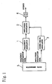
- Figure 1 shows a frequency modulator 1, an amplitude modulator 2, a sigma-delta modulator 3, a band pass filter 4, and a data generator 5.
- the data generator 5 is means of outputting vector modulation data constituted by frequency modulation data that is a digital signal, i.e., that has discrete values, and amplitude modulation data that is a digital signal, i.e., that has discrete values.
- the frequency modulator 1 is means of performing the frequency modulation of a signal at the carrier frequency with the frequency modulation data.
- the sigma-delta modulator 3 is a high-order sigma-delta modulator, and is means of performing the sigma-delta modulation of the amplitude modulation data, and outputting the digital amplitude data with a number of bits smaller than that of the amplitude modulation data.
- the amplitude modulator 2 is means of performing the amplitude modulation of an output signal of the frequency modulator 1 with the digital amplitude data outputted from the sigma-delta modulator 3.
- the band pass filter 4 is means of reducing an unnecessary frequency component from an output of the amplitude modulator 2. Although two band pass filters are necessary in the transmitting circuit apparatus using the conventional orthogonal modulator shown in Figure 14 , only one band pass filter is used in this embodiment. Thus, in the configuration of this embodiment, the number of the used band pass filters can be reduced in comparison with the conventional configuration.
- the data generator 5 generates vector modulation data.
- the data generator 5 generates the frequency modulation data, which is a digital signal, and the amplitude modulation data, which is a digital signal as vector modulation data, and outputs these.
- the frequency modulator 1 performs the frequency modulation of a signal at the carrier frequency with the frequency modulation data outputted from the data generator 5.
- An example of the signal that is given frequency modulation in the frequency modulator 1 is shown in Figure 11A . It can be seen that the signal that is given frequency modulation becomes a signal with a constant envelope.
- the sigma-delta modulator 3 is a high-order sigma-delta modulator, performs the sigma-delta modulation of the amplitude modulation data, and outputs the digital amplitude data with a number of bits smaller than that of the amplitude modulation data.
- the amplitude modulation data in an input of the sigma-delta modulator 3 is shown in Figure 11B .
- the amplitude modulation data is transmitted via a bus line where respective bits of data are transmitted with a plurality of signal lines with synchronizing with a clock signal, and is inputted into the sigma-delta modulator 3.
- output data from the sigma-delta modulator 3 is shown in Figure 11C .
- output data from the sigma-delta modulator 3 is modulated with binary digital amplitude data.
- amplitude modulation data is transmitted via a bus line as shown in Figure 11B
- the amplitude modulation data may be transmitted as an analog signal with multiple values that has discrete voltage values.
- an AD converter corresponding to characteristics of the sigma-delta modulator 3 shall be used instead of the sigma-delta modulator 3.
- the amplitude modulator 2 performs the amplitude modulation of an output signal of the frequency modulator 1 with digital amplitude data.
- An output of the amplitude modulator 2 is outputted after its unnecessary frequency component is reduced by a band pass filter.
- the output of the frequency modulator 1 is a signal that is given frequency modulation
- the output is a signal with a constant envelope.
- the amplitude modulator 2 performs amplitude modulation with values of digital amplitude data, what is necessary is to output only some kinds of output levels proportional to numeric values of the data since the number of bits of the digital amplitude data is small. Therefore, even if an amplitude modulator with low linearity is used, it is possible to easily perform level calibration.
- an amplitude modulator may be enough so long as it operates as a switch, and then, since it becomes possible to use the amplitude modulator 2 in a state near saturation, high efficiency can be obtained.
- there are few components depending on analog characteristics it becomes possible to obtain characteristics with sufficient linearity even if devices having large distortion are used.
- a structural example of the amplitude modulator 2 is shown in Figure 2A .
- a power supply controller 22 is controlled with binary digital amplitude data, and changes a supply voltage of an amplifier 21 stepwise to make the mean amplitude of an output signal proportional to each level of digital amplitude data.
- output amplitude only several kinds of levels may be specified. Since the amplifier 21 only amplifies a carrier wave that is a sinusoidal wave, distortion except harmonics does not arise fundamentally. Therefore, even if the amplifier 21 is used under an operating condition near saturation, distortion generated near a transmitted output is small. In addition, since a current hardly flows in an OFF state, high efficiency can be attained.
- Figure 12A is the conceptual diagram showing that an amplifier with an input-output characteristic 63 amplifies an input signal 61, and outputs an output signal 62.
- the input signal 61 is an analog signal, and its input-output characteristic 63 is nonlinear.
- Figure 12B is the conceptual diagram showing that an amplifier with an input-output characteristic 66 amplifies an input signal 64, and outputs an output signal 65.
- the input signal 64 is a digital signal whose voltage changes stepwise, and its input-output characteristic 66 is nonlinear.
- a supply voltage is a digital signal that has stepwise values
- the amplifier 21 Since the amplifier 21 only amplifies a carrier wave, which is a sinusoidal wave, in each stepwise voltage state, distortion except harmonics does not arise fundamentally.
- a carrier wave 67 which the amplifier 21 amplifies is shown in Figure 13 .
- the carrier wave 67 is a signal whose sinusoidal amplitude changes stepwise. For this reason, at each step, even if the amplifier 21 had the nonlinear characteristic when amplifying the carrier wave 67, distortion except harmonics would not arise. Therefore, even if the amplifier 21 is used under an operating condition near saturation, distortion generated near a transmitted output is small. In addition, a current hardly flows in an OFF state. Therefore, high efficiency can be obtained.
- FIG. 2B Another structural example of the amplitude modulator 2 is shown in Figure 2B .
- An amplitude modulator 23 is controlled with digital amplitude data.
- a carrier wave is controlled by the amplitude modulator 23, and is inputted into the amplifier 21 to be amplified. Power consumption at the time of an input in an OFF state can be reduced by making the amplifier 23 operate under bias conditions near class B or class C operation.
- Figure 2C shows a structural example where positions of the amplitude modulator 23 and an amplifier 21 in Figure 2B are replaced mutually. Since the amplifier 23 amplifies a carrier wave with operating under conditions near saturation at the time of the maximum output, consumption current is small and a power supply of the amplifier itself is not fluctuated, and hence stable operation is possible.
- An amplifier 21 is an amplifier using a dual gate FET 25.
- a carrier wave is inputted into a first gate, and is amplified and outputted.
- Digital amplitude data is inputted into a second gate, and controls an output level of the amplifier 25 stepwise. It is possible to easily obtain a high-speed control characteristic and a high-gain amplification characteristic by using the dual gate FET.
- Figures 3A and 3B Structural examples of the frequency modulator 1 are shown in Figures 3A and 3B . That is, Figure 3A shows a voltage-controlled oscillator 31, a variable frequency divider 32, a phase comparator 33, a loop filter 34, and a sigma-delta modulator 35.
- the sigma-delta modulator 35 may have the same configuration as that of the sigma-delta modulator 3 in Figure 1 fundamentally.
- An output of the voltage-controlled oscillator 31 is divided by the variable frequency divider 32, is given phase comparison to a reference signal by the phase comparator 33, passes through the loop filter 34, and controls an output frequency of the voltage-controlled oscillator 31.
- the sigma-delta modulator 35 performs the sigma-delta modulation of the data obtained by adding frequency modulation data and frequency channel data to output the data as a number of frequency division by the variable frequency divider 32.
- the sigma-delta modulator 35 operates at the same frequency as that of the reference signal.
- the frequency channel data means data expressing a frequency of a channel used for transmission among respective channels assigned to the transmission frequency bands.
- the pass bandwidth of the loop filter 34 is larger than the frequency bandwidth of frequency modulation data, and sufficiently smaller than the frequency of the reference signal. Therefore, frequency modulation according to frequency modulation data is given to the output of the voltage-controlled oscillator 31, and an unnecessary high-frequency component generated by the sigma-delta modulator 35 is reduced by the loop filter 34. According to this configuration, since a phase-locked loop can operate with following the frequency modulation data even when the change of an output frequency to a control voltage of the voltage-controlled oscillator 31 is not linear, an accurate frequency modulation output can be obtained.
- a set of phase comparator 33, loop filter 34, voltage-controlled oscillator 31, and a variable frequency divider 32 of this embodiment is an example of a phase-locked oscillator
- the sigma-delta modulator 35 of this embodiment is an example of the second sigma-delta modulator.
- Figure 3B shows a mixer 36, a local oscillator 37, and an IF modulator 38.
- the local oscillator 37 outputs a channel selection signal according to a desired channel frequency.
- the IF modulator 38 generates a modulation signal at an IF frequency that is modulated by frequency modulation data.
- An output of the voltage-controlled oscillator 31 is given frequency modulation into the IF frequency with the channel selection signal in the mixer 36, is given phase comparison to an output signal of the IF modulator 38 by the phase comparator 33, passes through the loop filter 34, and controls an output frequency of the voltage-controlled oscillator 31.
- Figure 4 shows a secondary integrator 41, a quantizer 42, a feedback circuit 43, a multiplier 47, and an adder 48.
- the quantizer 42 quantizes an output of the secondary integrator 41 by a quantization unit L and outputs it.
- the quantized output value is multiplied by the quantization unit L in the multiplier 47 trough the feedback circuit 43, is added to an input value in the adder 48, is inputted into the secondary integrator 41, and is given second-order integration to be outputted.
- A(z) z -1 / (1 - z -1 ) 2 .
- B(z) [(1 - z -1 ) 2 1]/z -1 .
- z -1 means a one clock delay element, and can be realized with a D flip-flop.
- the quantizer 42 divides an input value by the quantization unit L, and outputs an integer part of a quotient so that a remainder may not become negative.
- FIG. 4B A structural example of the second-order integrator 41 is shown in Figure 4B .
- An adder 51 and a delay circuit 52 constitute a first-order integrator.
- An output of the delay circuit 52 is added to an input value X1 in the adder 51, and an output of the adder 51 is inputted into the delay circuit 52.
- This first-order integrator is expressed in 1/ (1 - z -1 ) by z-transform.
- an adder 53 and a delay circuit 54 constitute a first-order integrator.
- An output of the adder 51 is inputted into the adder 53, an output of the delay circuit 54 is added to it, and an output of the adder 53 is inputted into the delay circuit 54.
- An output of the delay circuit 54 becomes an output value X2 of the second-order integrator.
- the delay circuits 52 and 54 output input values with delaying them by one clock. Since an output of the delay circuit 54 is used for an output of the second-order integrator, the whole circuit of the second-order integrator is expressed in z -1 / (1 - z -1 ) 2 by z-transform.
- is expressed in
- f 3 is a clock frequency.
- quantizingnoise Q is multiplied by the frequency characteristic of
- Figure 5 Another structural example of a second-order sigma-delta modulator is shown in Figure 5 . That is, Figure 5 shows adders 141, 142, 144, and 145, delay circuits 143, 146, and 148, a multiplier 149, and a quantizer 147.
- the quantizer 147 quantizes an output of the adder 145 by the quantization unit L and outputs it.
- the adder 142 and delay circuit 143 constitute a first first-order integrator, and the adder 145 and delay circuit 146 constitute a second first-order integrator.
- An output of the quantizer 147 passes through the delay circuit 148, and is multiplied by the quantization unit L by the multiplier 149 to be inputted into the adders 141 and 144.
- An output of the multiplier 149 inputted into the adder 141 is subtracted from the input value F of a sigma-delta modulator, is added to an output of the delay circuit 143 in the adder 142, and is inputted into the adders 144 and 143.
- An output of the adder 142 inputted into the adder 144 is given the subtraction of an output of the multiplier 149, is given the addition of an output of the delay circuit 146 in the adder 145, and is inputted into the delay circuit 146 and quantizer 147.
- the same characteristics as those in Figure 4 are demonstrated.
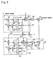
- Figure 6 shows the configuration of a sigma-delta modulator where two stages of sigma-delta modulators in Figure 4 are used. That is, Figure 6 shows a first second-order sigma-delta modulator 200, a second second-order sigma-delta modulator 220, and a second-order differential circuit 230.
- the first second-order sigma-delta modulator 200 comprises a second-order integrator 201, a quantizer 202, a feedback circuit 203, a multiplier 207, and an adder 208
- the feedback circuit 203 comprises a delay circuit 204, a doubling circuit 205, and an adder 206.
- the second-order sigma-delta modulator 220 comprises a second-order integrator 221, a quantizer 222, a feedback circuit 223, a multiplier 227, and an adder 228, and the feedback circuit 223 comprises a delay circuit 224, a doubling circuit 225, and an adder 226.
- the first second-order sigma-delta modulator 200 and second second-order sigma-delta modulator 220 have the same configuration as that in Figure 5A , and detailed description will be omitted.
- the data of a fraction part that is inputted from the external is inputted into the first second-order sigma-delta modulator 200.
- An output of the quantizer 202 of the first second-order sigma-delta modulator 200 is connected to the delay circuit 209.
- the adder 210 subtracts an output of the quantizer 202 of the first second-order sigma-delta modulator 200 from an input of the quantizer 202, and outputs its remainder to the multiplier 211.
- the multiplier 211 multiplies an output of the adder 210 by the quantization unit L, and outputs its product to the second second-order sigma-delta modulator 220.
- the second-order differential circuit 230 comprises a delay circuit 231, an adder 232, a delay circuit 233, and an adder 234.
- the delay circuit 231 and adder 232, and the delay circuit 233 and adder 234 constitute respective first-order differential circuits.
- An input of the second-order differential circuit 230 is inputted into the delay circuit 231 and adder 232.
- the adder 232 subtracts an output of the delay circuit 231 from the input of the second-order differential circuit 230, and outputs its remainder to the delay circuit 233 and adder 234 that are the following stages.
- the adder 234 subtracts an output of the delay circuit 233 from the output of the adder 232 that is the output of the preceding stage, and outputs its remainder.
- the adder 240 adds an output of the delay circuit 209 to the output of the second-order differential circuit 230, and makes its sum an output of the whole circuit.
- the operation of the sigma-delta modulator constituted as described above will be described below.
- an output of the first second-order sigma-delta modulator 200 be Y 1 and letting a quantizing error arising in the quantizer 202 be Q 1
- F 2 LQ 1
- Y 2 z -1 Q 1 + (1 - z -1 ) 2 Q 2 .
- n and m that are one or more, when combining a first n-th order sigma-delta modulator and a second m-th order sigma-delta modulator, by adjusting the delay of an output of the first n-th order sigma-delta modulator by providing an n-th order differential circuit in an output of the second m-th order sigma-delta modulator, it is possible to make them a (n+m)-th order sigma-delta modulator as a whole. It is apparent that it is also possible to combine three or more modulators similarly.
- Figure 7 shows first-order integrators 251, 252, 253, 254, and 255, adders 258, 259, and 260, coefficient multipliers 256, 257, 261, 262, 263, 264, and 265, a quantizer 267, and a multiplier 268.
- the quantizer 267 quantizes an output of the adder 266, and the quantizer 268 outputs a value obtained by the multiplication of the quantization unit L to the adder 258.
- the adder 258 subtracts an output of the quantizer 267 from an input value of the sigma-delta modulator.
- the first-order integrator 251 performs the first-order integration of an output of the adder 258.
- the adder 259 adds an output of the first-order integrator 251 to an output of the coefficient multiplier 256.
- the first-order integrator 252 performs the first-order integration of an output of the adder 259.
- An output of the first-order integrator 252 is given first-order integration by the first-order integrator 253 and is multiplied by a coefficient by the coefficient multiplier 256.
- the adder 260 adds an output of the first-order integrator 253 to an output of the coefficient multiplier 257.
- the first-order integrator 254 performs the first-order integration of an output of the adder 260.
- An output of the first-order integrator 254 is given first-order integration by the first-order integrator 255 and is multiplied by a coefficient by the coefficient multiplier 257.
- Outputs of the first-order integrators 251 to 255 are multiplied by coefficients by the coefficient multipliers 261 to 265 respectively, and are added by the adder 266 to be inputted into the quantizer 267. According to this configuration, it is possible to arbitrarily change frequency characteristics of sigma-delta modulation by arbitrarily setting a coefficient of each coefficient multiplier.
- FIG. 8 An example of frequency characteristics of quantizing noise to the order of sigma-delta modulators is shown in Figure 8 .
- the quantizing noise level in a low-frequency range is reduced. That is, it is possible to obtain an output, where the increase of quantizing noise is suppressed, in a low-frequency range even if the output has the number of bits coarser than an input value.
- an improvement factor can be enhanced by making a clock frequency high.
- Figure 9 shows another embodiment of a transmitting circuit apparatus according to the present invention.
- Figure 9 shows the configuration corresponding to the case that a frequency modulator and an amplitude modulator of the transmitting circuit apparatus in Figure 1 are connected with an optical fiber. Since the contents shown in Figures 2 to 7 are applicable similarly, detailed description will be omitted.
- Figure 9 shows a data generator 301, a frequency modulator 302, a sigma-delta modulator 303, E/O converters 304 and 305, a optical frequency synthesizer 306, a branching filter 307 , O/E converters 308 and 309 , an amplitude modulator 310, a band pass filter 311, an antenna 312, and an optical fiber 313.
- Outputs of the frequency modulator 302 and sigma-delta modulator 303 are converted into optical signals with E/O converters 304 and 305, respectively.
- the E/O converters 304 and 305 are laser diodes, and output light whose wavelengths differ from each other.
- Frequency modulation data outputted from the data generator 301 is given frequency modulation by the frequency modulator 302, and is inputted into the E/O converter 304.
- amplitude modulation data outputted from the data generator 301 is given sigma-delta modulation by the sigma-delta modulator 303 to become digital amplitude data, and is inputted into the E/O converter 305.
- Outputs of the E/O converters 304 and 305 are synthesized by the optical frequency synthesizer 306, the signal is transmitted within the optical fiber 313 and is branched by the branching filter 307 for every wave length, and the signals are inputted into O/E converters 308 and 309, respectively.
- the O/E converters 308 and 309 are photo diodes, and convert optical signals inputted into respective converters into a frequency modulation signal and digital amplitude data that are electric signals.
- the frequency modulation signal is given frequency modulation with the digital amplitude data by the amplitude modulator 310, its unnecessary frequency component is reduced by the band pass filter 311, and the frequency modulation signal is outputted from the antenna 312.
- a frequency modulation signal with a constant envelope, and a digital signal are transmitted in a transmission part of an optical signal. Therefore, it is possible to enlarge tolerance to a distorted characteristic in the optical transmission part from an E/O converter to an O/E converter. In addition, it is possible to minimize signal processing after restoring to an electric signal by performing transmission after sigma-delta modulation without transmitting amplitude modulation data in a baseband digital signal with a large number of bits as it is. Furthermore, since the power consumption of an amplitude modulator is made small like the first embodiment, it is possible to realize a small optical base station system with low power consumption.
- Figure 10 shows the configuration where a method of transmitting an optical signal differs from the configuration in Figure 9 .
- the same reference numerals are assigned to the same parts as those in Figure 9 , and detailed description will be omitted. That is, Figure 10 shows a synthesizer 321, an E/O converter 322, an O/E converter 323, and a branching filter 324.
- An output signal of the frequency modulator 302 and digital amplitude data that is an output signal of the sigma-delta modulator 303 are synthesized by the synthesizer 321, and are converted into an optical signal by the E/O converter 322.
- the converted optical signal is transmitted through the optical fiber 313, and is converted into an electric signal by the O/E converter 323.
- An output of the O/E converter 323 is divided into a frequency modulation signal and digital amplitude data by the branching filter 324.
- the frequency modulation signal is given frequency modulation with the digital amplitude data by the amplitude modulator 310, its unnecessary frequency component is reduced by the band pass filter 311, and the frequency modulation signal is outputted from the antenna 312.
- a transmitting circuit apparatus with sufficient linearity and low power consumption by outputting a carrier wave that is given frequency modulation by a frequency modulator, performing the sigma-delta modulation of amplitude modulation data by a sigma-delta modulator, performing the amplitude modulation of the carrier wave, which is given frequency modulation by the amplitude modulator, with signal that is given sigma-delta modulation, and outputting the signal.
- the present invention can provide a transmitting circuit apparatus having good linearity, high transmission output power efficiency, and small power consumption.
- the present invention can also obtain the following effects with the above-described effect.
- the present invention can provide a transmitting circuit apparatus with the highest transmission output power efficiency, and the smallest power consumption.
- the present invention can provide a transmitting circuit apparatus which can control a grade of increase of quantizing noise according to its order.
- the present invention when having a band pass filter that reduces the unnecessary signal outside a transmission frequency band of an output signal of an amplitude modulator, can provide a transmitting circuit apparatus that can reduce an unnecessary frequency component resulting from quantizing noise peculiar to a sigma-delta modulator.
- the present invention can provide a transmitting circuit apparatus with further high efficiency, wherein an amplitude modulator has a power amplifier and performs amplitude modulation by controlling a power supply of the power amplifier on the basis of an output signal of the sigma-delta modulator.
- the present invention can provide a transmitting circuit apparatus with still further high efficiency, wherein an output of an amplitude modulator is equipped with a power amplifier in class B or class C operation.
- the present invention can provide a transmitting circuit apparatus which obtains an accurate frequency modulation output, wherein a frequency modulator has a phase-locked oscillator, which include at least a variable frequency divider, and a second sigma-delta modulator, wherein the second sigma-delta modulator outputs a value, which is obtained by performing the second-order or higher sigma-delta modulation of the data obtained by adding frequency modulation data to carrier frequency data, as a number of division of the variable frequency divider, and wherein a carrier wave which is given frequency modulation is outputted from the phase-locked oscillator.
- a frequency modulator has a phase-locked oscillator, which include at least a variable frequency divider, and a second sigma-delta modulator, wherein the second sigma-delta modulator outputs a value, which is obtained by performing the second-order or higher sigma-delta modulation of the data obtained by adding frequency modulation data to carrier frequency data, as a number of division of the variable
- the present invention can provide a transmitting circuit apparatus, which can prevent the degradation of a noise characteristic by frequency conversion even if a general orthogonal modulator is used, wherein a frequency modulator has a phase comparator, a loop filter, a voltage-controlled oscillator, a mixer, and an IF modulator, wherein the IF modulator outputs a modulated wave signal at an intermediate frequency that is frequency-modulated with the frequency modulation data, wherein the mixer performs frequency conversion of an output signal of the voltage-controlled oscillator to an intermediate frequency with a channel selection signal, wherein the phase comparator performs phase comparison of the frequency-converted signal to a modulated wave signal at the intermediate frequency, wherein the loop filter reduces an unnecessary signal from the phase-compared signal, and wherein the voltage-controlled oscillator outputs the frequency-modulated carrier wave by its oscillation frequency being controlled by the signal where the unnecessary signal is reduced.
- the present invention can provide a transmitting circuit apparatus that can enlarge tolerance to distortion characteristics in an optical fiber and can transmit an optical signal via one optical fiber, comprising: a first E/O converter which converts the frequency-modulated carrier wave from an electric signal into an optical signal; a first O/E converter which is connected to the first E/O converter via an optical fiber and converts the optical signal, which is converted by the first E/O converter, into an electric signal; a second E/O converter which converts an output signal of the sigma-delta modulator into an optical signal whose wavelength is different from that of an output of the first E/O converter; and a second O/E converter which is connected to the second E/O converter via the optical fiber and converts an optical signal, which is converted by the second E/O converter, into an electric signal, wherein an output signal of the second E/O converter is synthesized with an output signal of the first E/O converter, and is branched after being transmitted via the optical fiber to be converted into an electric signal from the optical signal by the second
- the present invention can provide a transmitting circuit apparatus that can transmit an optical signal by using only one O/E converter and one E/O converter, comprising: an E/O converter which converts a signal, which is obtained by synthesizing a carrier wave, which is frequency-modulated by the frequency modulator, and amplitude data, which has digital values which are outputted from the sigma-delta modulator, from an electric signal into an optical signal; and an O/E converter which is connected to the E/O converter via an optical fiber and converts a converted signal from an optical signal into an electric signal, wherein a signal converted by the O/E converter is divided into the frequency-modulated carrier wave and the amplitude data by a filter, and wherein the amplitude modulator performs amplitude modulation of the frequency-modulated carrier wave, which is separated, with the amplitude data that is separated.
- the present invention can provide a transmitting circuit apparatus that can arbitrarily change a frequency characteristic, wherein a sigma-delta modulator has an n-th integrator generating a signal obtained by performing n-th integration of the amplitude modulation data, a quantizer which quantizes the n-th-integrated signal into a digital value, and a feedback circuit which feeds back the quantized value to an input value of the sigma-delta modulator, wherein the quantized digital value becomes an output of the sigma-delta modulator, and wherein the fed-back value is added to the input value of the sigma-delta modulator and is inputted into the n-th integrator.
- the present invention can provide a transmitting circuit apparatus that can realize a higher-order sigma-delta modulator and hence can further reduce a distortion component caused by quantization noise, wherein the sigma-delta modulator has a plurality of low-order sigma-delta modulators that is connected in multiple stages, and wherein outputs of the plurality of low-order sigma-delta modulators are connected to a differentiator including configuration expressed in (1 - z -1 ) m by z-transform to an order m until the preceding stage respectively, and are synthesized.
Landscapes
- Engineering & Computer Science (AREA)
- Computer Networks & Wireless Communication (AREA)
- Signal Processing (AREA)
- Power Engineering (AREA)
- Compression, Expansion, Code Conversion, And Decoders (AREA)
Claims (6)
- Appareil à circuits de transmission comprenant :- un modulateur sigma-delta (3) adapté à effectuer une modulation sigma delta de données de modulation d'amplitude afin de produire en sortie des données numériques d'amplitudes ; et- un modulateur d'amplitude (2) comprenant un amplificateur (21) et un dispositif de commande d'alimentation électrique (22) adapté à changer une tension d'alimentation de l'amplificateur (21) ;- dans lequel :- l'appareil à circuits de transmission comprend en outre un modulateur de fréquence (1) adapté à effectuer une modulation de fréquence d'une onde porteuse avec des données de modulation de fréquence et à produire en sortie l'onde porteuse modulée en fréquence ; et- le modulateur d'amplitude (2) est adapté à effectuer une modulation d'amplitude de l'onde porteuse modulée en fréquence par le dispositif de commande d'alimentation (22) adapté à changer la tension d'alimentation de l'amplificateur de puissance (21) en se fondant sur les données numériques d'amplitudes produites en sortie ;- caractérisé en ce que :- le modulateur d'amplitude est adapté à effectuer la modulation d'amplitude de telle sorte qu'une amplitude moyenne du signal de sortie de l'amplificateur devienne proportionnelle à chaque niveau des données numériques d'amplitudes produites en sortie.
- Appareil à circuits de transmission selon la revendication 1, dans lequel le modulateur sigma-delta (3) est un modulateur sigma-delta au moins du second ordre ou d'un ordre plus élevé.
- Appareil à circuits de transmission selon la revendication 1 ou 2 :- dans lequel le modulateur de fréquence (1) comporte un oscillateur asservi en phase, qui inclut au moins un diviseur de fréquence variable (32), et un second modulateur sigma-delta (35) ;- dans lequel le second modulateur sigma-delta (35) est adapté à produire en sortie une valeur, qui est obtenue en effectuant une modulation sigma-delta, du second ordre ou d'un ordre plus élevé, de données obtenues en additionnant les données de modulation de fréquence à des données de fréquence de porteuse, comme facteur de division du diviseur de fréquence variable (32) ; et- dans lequel l'onde porteuse modulée en fréquence est délivrée en sortie de l'oscillateur asservi en phase.
- Appareil à circuits de transmission selon la revendication 1 ou 2 :- dans lequel le modulateur de fréquence (1) comporte un comparateur de phase (33), un filtre en boucle (34), un oscillateur commandé par tension (31), un mélangeur (36) et un modulateur à fréquence intermédiaire IF (38) ;- dans lequel le modulateur IF (38) est adapté à produire en sortie un signal d'onde modulée à une fréquence intermédiaire qui est une modulation de fréquence donnée avec les données de modulation de fréquence ;- dans lequel le mélangeur (3) est adapté à effectuer une conversion de fréquence d'un signal de sortie de l'oscillateur commandé par tension (31) en une fréquence intermédiaire avec un signal de sélection de canal ;- dans lequel le comparateur de phase (33) est adapté à effectuer une comparaison de phase entre le signal converti en fréquence et un signal d'onde modulée à la fréquence intermédiaire ;- dans lequel le filtre en boucle (34) est adapté à réduire un signal inutile du signal ayant fait l'objet d'une comparaison de phase ; et- dans lequel l'oscillateur commandé par tension (31) est adapté à produire en sortie l'onde porteuse modulée en fréquence grâce au fait que sa fréquence d'oscillation est commandée par le signal dans lequel le signal inutile est réduit.
- Appareil à circuits de transmission selon la revendication 1, comprenant :- un premier convertisseur électro/optique (304) adapté à convertir l'onde porteuse modulée en fréquence d'un signal électrique en un signal optique ;- un premier convertisseur opto/électrique (308) connecté au premier convertisseur électro/optique via une fibre optique (313) et adapté à convertir un signal optique, obtenu par la conversion du premier convertisseur électro/optique (304), en un signal électrique ;- un second convertisseur électro/optique (305) adapté à convertir un signal de sortie du modulateur sigma-delta (303) en un signal optique dont la longueur d'onde est différente de celle d'une sortie du premier convertisseur électro/optique (304) ; et- un second convertisseur opto/électrique (309) connecté au second convertisseur électro/optique (305) via la fibre optique (313) et adapté à convertir un signal optique, obtenu par la conversion du second convertisseur électro/optique (305), en un signal électrique ;- dans lequel un signal de sortie du second convertisseur électro/optique (305) est synthétisé avec un signal de sortie du premier convertisseur électro/optique (304) et est ramifié, après avoir été transmis via la fibre optique (313), pour être converti en un signal électrique à partir du signal optique par le second convertisseur opto/électrique (309) ; et- dans lequel le modulateur d'amplitude (310) est adapté à effectuer une modulation d'amplitude d'un signal de sortie du premier convertisseur opto/électrique (308) avec un signal de sortie du second convertisseur opto/électrique (309).
- Appareil à circuits de transmission selon la revendication 1, comprenant :- un convertisseur électro/optique (322) adapté à convertir un signal, obtenu en synthétisant une onde porteuse, laquelle fait l'objet de la modulation de fréquence par le modulateur de fréquence (302), et des données d'amplitudes ayant des valeurs numériques produites en sortie du modulateur sigma-delta (303), d'un signal électrique en un signal optique ; et- un convertisseur opto/électrique (323) connecté au convertisseur électro/optique (322) via une fibre optique (313) et adapté à convertir un signal converti d'un signal optique en un signal électrique, dans lequel un signal converti par le convertisseur opto/électrique (323) est divisé en l'onde porteuse modulée en fréquence et les données d'amplitudes par un filtre ;- dans lequel le modulateur d'amplitude (310) est adapté à effectuer une modulation d'amplitude de l'onde porteuse modulée en fréquence, qui est séparée, avec les données d'amplitudes qui sont séparées.
Applications Claiming Priority (2)
| Application Number | Priority Date | Filing Date | Title |
|---|---|---|---|
| JP2001047447 | 2001-02-22 | ||
| JP2001047447 | 2001-02-22 |
Publications (3)
| Publication Number | Publication Date |
|---|---|
| EP1235403A2 EP1235403A2 (fr) | 2002-08-28 |
| EP1235403A3 EP1235403A3 (fr) | 2006-05-24 |
| EP1235403B1 true EP1235403B1 (fr) | 2012-12-05 |
Family
ID=18908876
Family Applications (1)
| Application Number | Title | Priority Date | Filing Date |
|---|---|---|---|
| EP02003833A Expired - Lifetime EP1235403B1 (fr) | 2001-02-22 | 2002-02-20 | Modulation combinée en fréquence et en amplitude |
Country Status (3)
| Country | Link |
|---|---|
| US (1) | US7013090B2 (fr) |
| EP (1) | EP1235403B1 (fr) |
| CN (1) | CN1233138C (fr) |
Families Citing this family (68)
| Publication number | Priority date | Publication date | Assignee | Title |
|---|---|---|---|---|
| US6975687B2 (en) | 2000-06-16 | 2005-12-13 | Hughes Electronics Corporation | Linearized offset QPSK modulation utilizing a sigma-delta based frequency modulator |
| US7546097B2 (en) * | 2002-03-06 | 2009-06-09 | Qualcomm Incorporated | Calibration techniques for frequency synthesizers |
| US7663762B2 (en) | 2002-07-09 | 2010-02-16 | Finisar Corporation | High-speed transmission system comprising a coupled multi-cavity optical discriminator |
| US7263291B2 (en) * | 2002-07-09 | 2007-08-28 | Azna Llc | Wavelength division multiplexing source using multifunctional filters |
| US6963685B2 (en) * | 2002-07-09 | 2005-11-08 | Daniel Mahgerefteh | Power source for a dispersion compensation fiber optic system |
| JP4214850B2 (ja) * | 2002-08-20 | 2009-01-28 | ソニー株式会社 | ディジタル信号処理装置及びディジタル信号処理方法 |
| US7054538B2 (en) * | 2002-10-04 | 2006-05-30 | Azna Llc | Flat dispersion frequency discriminator (FDFD) |
| WO2004034565A2 (fr) * | 2002-10-08 | 2004-04-22 | M/A-Com, Inc. | Appareil, procedes et articles de fabrication pour le traitement de signaux a bande large |
| US7545865B2 (en) | 2002-12-03 | 2009-06-09 | M/A-Com, Inc. | Apparatus, methods and articles of manufacture for wideband signal processing |
| US7555225B2 (en) * | 2002-11-06 | 2009-06-30 | Finisar Corporation | Optical system comprising an FM source and a spectral reshaping element |
| US7564889B2 (en) * | 2002-11-06 | 2009-07-21 | Finisar Corporation | Adiabatically frequency modulated source |
| US7406266B2 (en) * | 2002-11-06 | 2008-07-29 | Finisar Corporation | Flat-topped chirp induced by optical filter edge |
| US7505694B2 (en) * | 2002-11-06 | 2009-03-17 | Finisar Corporation | Thermal chirp compensation systems for a chirp managed directly modulated laser (CML™) data link |
| US7536113B2 (en) * | 2002-11-06 | 2009-05-19 | Finisar Corporation | Chirp managed directly modulated laser with bandwidth limiting optical spectrum reshaper |
| US7558488B2 (en) * | 2002-11-06 | 2009-07-07 | Finisar Corporation | Reach extension by using external Bragg grating for spectral filtering |
| US7742542B2 (en) * | 2002-11-06 | 2010-06-22 | Finisar Corporation | Phase correlated quadrature amplitude modulation |
| US7280721B2 (en) * | 2002-11-06 | 2007-10-09 | Azna Llc | Multi-ring resonator implementation of optical spectrum reshaper for chirp managed laser technology |
| US7925172B2 (en) * | 2002-12-03 | 2011-04-12 | Finisar Corporation | High power, low distortion directly modulated laser transmitter |
| US7474859B2 (en) * | 2002-12-03 | 2009-01-06 | Finisar Corporation | Versatile compact transmitter for generation of advanced modulation formats |
| US7907648B2 (en) * | 2002-12-03 | 2011-03-15 | Finisar Corporation | Optical FM source based on intra-cavity phase and amplitude modulation in lasers |
| US7542683B2 (en) | 2002-12-03 | 2009-06-02 | Finisar Corporation | Chirp Managed Laser (CML) transmitter |
| US7613401B2 (en) * | 2002-12-03 | 2009-11-03 | Finisar Corporation | Optical FM source based on intra-cavity phase and amplitude modulation in lasers |
| US7860404B2 (en) * | 2002-12-03 | 2010-12-28 | Finisar Corporation | Optical FM source based on intra-cavity phase and amplitude modulation in lasers |
| US7609977B2 (en) * | 2002-12-03 | 2009-10-27 | Finisar Corporation | Optical transmission using semiconductor optical amplifier (SOA) |
| US7480464B2 (en) * | 2002-12-03 | 2009-01-20 | Finisar Corporation | Widely tunable, dispersion tolerant transmitter |
| US7813648B2 (en) * | 2002-12-03 | 2010-10-12 | Finisar Corporation | Method and apparatus for compensating for fiber nonlinearity in a transmission system |
| US7809280B2 (en) * | 2002-12-03 | 2010-10-05 | Finisar Corporation | Chirp-managed, electroabsorption-modulated laser |
| US8792531B2 (en) * | 2003-02-25 | 2014-07-29 | Finisar Corporation | Optical beam steering for tunable laser applications |
| US7630425B2 (en) * | 2003-02-25 | 2009-12-08 | Finisar Corporation | Optical beam steering for tunable laser applications |
| JP2005210537A (ja) * | 2004-01-23 | 2005-08-04 | National Institute Of Information & Communication Technology | 光fsk変調器を用いたuwb信号の発生装置 |
| CA2557150A1 (fr) * | 2004-02-27 | 2005-09-15 | Azna Llc | Systeme optique comprenant une source fm et un element spectral de remise en forme |
| US7496151B2 (en) * | 2004-03-05 | 2009-02-24 | Panasonic Corporation | Transmitting circuit, communication equipment, audio equipment, video equipment, and transmitting method |
| US7639955B2 (en) | 2004-09-02 | 2009-12-29 | Finisar Corporation | Method and apparatus for transmitting a signal using a chirp managed laser (CML) and an optical spectrum reshaper (OSR) before an optical receiver |
| US7983632B2 (en) * | 2004-09-24 | 2011-07-19 | Broadcom Corporation | Feedback control loop for amplitude modulation in a polar transmitter with a translational loop |
| EP1803083B1 (fr) * | 2004-10-15 | 2012-02-29 | Nxp B.V. | Procede d'exploitation d'un systeme rfid |
| GB0426965D0 (en) * | 2004-12-09 | 2005-01-12 | Tang Bob | Methods to increase number of symbols in a transmission bit and to increase channel capacity in modulated transmissions, without needing to reduce signal |
| US20070012860A1 (en) * | 2005-05-05 | 2007-01-18 | Daniel Mahgerefteh | Optical source with ultra-low relative intensity noise (RIN) |
| US7362251B2 (en) | 2006-05-18 | 2008-04-22 | Broadcom Corporation | Method and system for digital to analog conversion for power amplifier driver amplitude modulation |
| US7697186B2 (en) * | 2006-10-24 | 2010-04-13 | Finisar Corporation | Spectral response modification via spatial filtering with optical fiber |
| WO2008080171A1 (fr) * | 2006-12-22 | 2008-07-03 | Finisar Corporation | Émetteur optique comportant un laser accordable à modulation directe et un élément de remise en forme de spectre optique périodique |
| US7941057B2 (en) * | 2006-12-28 | 2011-05-10 | Finisar Corporation | Integral phase rule for reducing dispersion errors in an adiabatically chirped amplitude modulated signal |
| US8131157B2 (en) * | 2007-01-22 | 2012-03-06 | Finisar Corporation | Method and apparatus for generating signals with increased dispersion tolerance using a directly modulated laser transmitter |
| WO2008097928A1 (fr) * | 2007-02-02 | 2008-08-14 | Finisar Corporation | Emballage stabilisant la température pour composants optoélectroniques dans un module d'émetteur |
| US8027593B2 (en) | 2007-02-08 | 2011-09-27 | Finisar Corporation | Slow chirp compensation for enhanced signal bandwidth and transmission performances in directly modulated lasers |
| US7991291B2 (en) * | 2007-02-08 | 2011-08-02 | Finisar Corporation | WDM PON based on DML |
| US7697847B2 (en) * | 2007-04-02 | 2010-04-13 | Finisar Corporation | Dispersion compensator for frequency reshaped optical signals |
| US7991297B2 (en) * | 2007-04-06 | 2011-08-02 | Finisar Corporation | Chirped laser with passive filter element for differential phase shift keying generation |
| US8204386B2 (en) * | 2007-04-06 | 2012-06-19 | Finisar Corporation | Chirped laser with passive filter element for differential phase shift keying generation |
| US7760777B2 (en) * | 2007-04-13 | 2010-07-20 | Finisar Corporation | DBR laser with improved thermal tuning efficiency |
| US8140028B2 (en) | 2007-05-10 | 2012-03-20 | Skyworks Solutions, Inc. | Low noise RF driver |
| US7778295B2 (en) * | 2007-05-14 | 2010-08-17 | Finisar Corporation | DBR laser with improved thermal tuning efficiency |
| US8838257B1 (en) * | 2007-10-04 | 2014-09-16 | Marvell International Ltd. | Controller and design support apparatus |
| US8160455B2 (en) * | 2008-01-22 | 2012-04-17 | Finisar Corporation | Method and apparatus for generating signals with increased dispersion tolerance using a directly modulated laser transmitter |
| US8260145B2 (en) | 2008-03-12 | 2012-09-04 | Deepnarayan Gupta | Digital radio frequency tranceiver system and method |
| US7869473B2 (en) * | 2008-03-21 | 2011-01-11 | Finisar Corporation | Directly modulated laser with isolated modulated gain electrode for improved frequency modulation |
| US8260150B2 (en) * | 2008-04-25 | 2012-09-04 | Finisar Corporation | Passive wave division multiplexed transmitter having a directly modulated laser array |
| ATE488117T1 (de) * | 2009-03-24 | 2010-11-15 | Alcatel Lucent | Verfahren zur datenübertragung mittels eines ummantelungseliminierungs- und - wiederherstellungsverstärkers, ummantelungseliminierungs- und - wiederherstellungsverstärker, übertragungsvorrichtung, empfangsvorrichtung und kommunikationsnetzwerk dafür |
| US8199785B2 (en) * | 2009-06-30 | 2012-06-12 | Finisar Corporation | Thermal chirp compensation in a chirp managed laser |
| JP5493227B2 (ja) | 2009-12-22 | 2014-05-14 | 富士通株式会社 | 送信回路 |
| CN102386929B (zh) * | 2011-09-22 | 2013-11-13 | 北京大学 | Sigma-Delta调制器及包括该调制器的Sigma-Delta模数转换器 |
| EP2618531B1 (fr) * | 2012-01-20 | 2014-12-24 | ADVA Optical Networking SE | Procédé et dispositif pour transmettre un signal à basse fréquence sur une liaison de transmission de données à l'aide d'un signal à débit binaire élevé numérique |
| US9479325B1 (en) * | 2013-04-12 | 2016-10-25 | Maxim Integrated Products, Inc. | Reduced frequency backwards clock for isolated sigma-delta modulators |
| US9356693B1 (en) * | 2013-04-12 | 2016-05-31 | Maxim Integrated Products, Inc. | Optical isolator preventive measure indicator |
| JP6090441B2 (ja) * | 2013-05-31 | 2017-03-08 | 日本電気株式会社 | 送信回路 |
| US9887705B2 (en) * | 2014-12-05 | 2018-02-06 | Nec Corporation | Delta-sigma modulator and modulation method, transmission device, and transmission method |
| KR20220098154A (ko) * | 2019-11-07 | 2022-07-11 | 구글 엘엘씨 | 조건부 전체 구성 및 조건부 델타 구성 |
| WO2023087219A1 (fr) * | 2021-11-18 | 2023-05-25 | 华为技术有限公司 | Dispositif d'amplification de puissance et dispositif de communication sans fil |
| CN119363055B (zh) * | 2024-12-24 | 2025-03-18 | 苏州泰莱微波技术有限公司 | 一种频率调节的射频放大器 |
Citations (1)
| Publication number | Priority date | Publication date | Assignee | Title |
|---|---|---|---|---|
| WO2000030245A1 (fr) * | 1998-11-18 | 2000-05-25 | Ericsson Inc. | Circuit et procede de modulation i/q avec modulation d'amplitude independante, tres efficace |
Family Cites Families (7)
| Publication number | Priority date | Publication date | Assignee | Title |
|---|---|---|---|---|
| JP2898435B2 (ja) * | 1991-05-21 | 1999-06-02 | 株式会社エイ・ティ・アール光電波通信研究所 | 無線リンク用光伝送システム |
| JP2616468B2 (ja) * | 1994-11-25 | 1997-06-04 | 日本電気株式会社 | 光マイクロセル伝送方式 |
| US6047029A (en) * | 1997-09-16 | 2000-04-04 | Telefonaktiebolaget Lm Ericsson | Post-filtered delta sigma for controlling a phase locked loop modulator |
| US5952895A (en) * | 1998-02-23 | 1999-09-14 | Tropian, Inc. | Direct digital synthesis of precise, stable angle modulated RF signal |
| US6061555A (en) * | 1998-10-21 | 2000-05-09 | Parkervision, Inc. | Method and system for ensuring reception of a communications signal |
| FI105609B (fi) * | 1998-10-27 | 2000-09-15 | Nokia Mobile Phones Ltd | Menetelmä ja järjestely lähetyssignaalin muodostamiseksi |
| US6590940B1 (en) | 1999-05-17 | 2003-07-08 | Ericsson Inc. | Power modulation systems and methods that separately amplify low and high frequency portions of an amplitude waveform |
-
2002
- 2002-02-20 EP EP02003833A patent/EP1235403B1/fr not_active Expired - Lifetime
- 2002-02-21 US US10/081,708 patent/US7013090B2/en not_active Expired - Lifetime
- 2002-02-21 CN CNB021032947A patent/CN1233138C/zh not_active Expired - Fee Related
Patent Citations (1)
| Publication number | Priority date | Publication date | Assignee | Title |
|---|---|---|---|---|
| WO2000030245A1 (fr) * | 1998-11-18 | 2000-05-25 | Ericsson Inc. | Circuit et procede de modulation i/q avec modulation d'amplitude independante, tres efficace |
Also Published As
| Publication number | Publication date |
|---|---|
| CN1233138C (zh) | 2005-12-21 |
| EP1235403A3 (fr) | 2006-05-24 |
| US7013090B2 (en) | 2006-03-14 |
| EP1235403A2 (fr) | 2002-08-28 |
| CN1372406A (zh) | 2002-10-02 |
| US20020186440A1 (en) | 2002-12-12 |
Similar Documents
| Publication | Publication Date | Title |
|---|---|---|
| EP1235403B1 (fr) | Modulation combinée en fréquence et en amplitude | |
| US6990155B2 (en) | Wireless quadrature modulator transmitter using E/O and O/E connectives | |
| US6717998B2 (en) | Frequency synthesizer apparatus equipped with fraction part control circuit, communication apparatus, frequency modulator apparatus, and frequency modulating method | |
| EP1345375B1 (fr) | Procédé et dispositif de modulation en fréquence | |
| US7953174B2 (en) | Radio transmission frequency digital signal generation | |
| JP5546812B2 (ja) | デルタ−シグマ・ディジタル/アナログ・コンバータ付きの効率的ハードウェアのトランシーバ | |
| US7230996B2 (en) | Transmitting circuit device and wireless communications device | |
| WO2005011109A1 (fr) | Appareil d'amplification | |
| US20050191976A1 (en) | Reconfigurable transmitter with direct digital to RF modulator | |
| KR101922108B1 (ko) | 병렬 구조의 디지털 무선 송신기 및 이를 포함하는 무선 통신 시스템 | |
| JP2002057732A (ja) | 送信回路装置 | |
| US8049651B2 (en) | ΔΣ modulation circuit and system | |
| US6784817B2 (en) | Data generating method, data generator, and transmitter using the same | |
| CN104620510A (zh) | 发射机 | |
| JP3878029B2 (ja) | 送信回路装置 | |
| US7502422B2 (en) | Electromagnetic wave transmitter systems, methods and articles of manufacture | |
| US7817725B2 (en) | Data converter device and data conversion method, and transmitter circuit, communications device and electronic device using the same | |
| US7460843B2 (en) | Amplifier apparatus, polar modulation transmission apparatus and wireless communication apparatus | |
| JP4076914B2 (ja) | データ生成方法、データ生成器、およびそれを用いた送信機 | |
| JP4128488B2 (ja) | 送信回路装置、及び無線通信装置 | |
| US20040128279A1 (en) | Data converter, signal generator, transmitter and communication apparatus using the data converter or the signal generator, and data conversion method | |
| JP2004159319A (ja) | データ変換器、信号発生器、それを用いた送信機および通信機器、データ変換方法 |
Legal Events
| Date | Code | Title | Description |
|---|---|---|---|
| PUAI | Public reference made under article 153(3) epc to a published international application that has entered the european phase |
Free format text: ORIGINAL CODE: 0009012 |
|
| AK | Designated contracting states |
Kind code of ref document: A2 Designated state(s): AT BE CH CY DE DK ES FI FR GB GR IE IT LI LU MC NL PT SE TR |
|
| AX | Request for extension of the european patent |
Free format text: AL;LT;LV;MK;RO;SI |
|
| PUAL | Search report despatched |
Free format text: ORIGINAL CODE: 0009013 |
|
| RIC1 | Information provided on ipc code assigned before grant |
Ipc: H04L 27/36 20060101AFI20060322BHEP |
|
| AK | Designated contracting states |
Kind code of ref document: A3 Designated state(s): AT BE CH CY DE DK ES FI FR GB GR IE IT LI LU MC NL PT SE TR |
|
| AX | Request for extension of the european patent |
Extension state: AL LT LV MK RO SI |
|
| 17P | Request for examination filed |
Effective date: 20060802 |
|
| AKX | Designation fees paid |
Designated state(s): DE FR GB |
|
| 17Q | First examination report despatched |
Effective date: 20070611 |
|
| RAP1 | Party data changed (applicant data changed or rights of an application transferred) |
Owner name: PANASONIC CORPORATION |
|
| REG | Reference to a national code |
Ref country code: DE Ref legal event code: R079 Ref document number: 60244144 Country of ref document: DE Free format text: PREVIOUS MAIN CLASS: H04L0027320000 Ipc: H03F0003240000 |
|
| RIC1 | Information provided on ipc code assigned before grant |
Ipc: H04L 27/36 20060101ALI20120321BHEP Ipc: H03F 3/24 20060101AFI20120321BHEP |
|
| GRAP | Despatch of communication of intention to grant a patent |
Free format text: ORIGINAL CODE: EPIDOSNIGR1 |
|
| GRAS | Grant fee paid |
Free format text: ORIGINAL CODE: EPIDOSNIGR3 |
|
| GRAA | (expected) grant |
Free format text: ORIGINAL CODE: 0009210 |
|
| AK | Designated contracting states |
Kind code of ref document: B1 Designated state(s): DE FR GB |
|
| REG | Reference to a national code |
Ref country code: GB Ref legal event code: FG4D |
|
| REG | Reference to a national code |
Ref country code: DE Ref legal event code: R096 Ref document number: 60244144 Country of ref document: DE Effective date: 20130131 |
|
| PLBE | No opposition filed within time limit |
Free format text: ORIGINAL CODE: 0009261 |
|
| STAA | Information on the status of an ep patent application or granted ep patent |
Free format text: STATUS: NO OPPOSITION FILED WITHIN TIME LIMIT |
|
| 26N | No opposition filed |
Effective date: 20130906 |
|
| REG | Reference to a national code |
Ref country code: FR Ref legal event code: ST Effective date: 20131031 |
|
| GBPC | Gb: european patent ceased through non-payment of renewal fee |
Effective date: 20130305 |
|
| REG | Reference to a national code |
Ref country code: DE Ref legal event code: R097 Ref document number: 60244144 Country of ref document: DE Effective date: 20130906 |
|
| PG25 | Lapsed in a contracting state [announced via postgrant information from national office to epo] |
Ref country code: GB Free format text: LAPSE BECAUSE OF NON-PAYMENT OF DUE FEES Effective date: 20130305 Ref country code: FR Free format text: LAPSE BECAUSE OF NON-PAYMENT OF DUE FEES Effective date: 20130228 |
|
| PGFP | Annual fee paid to national office [announced via postgrant information from national office to epo] |
Ref country code: DE Payment date: 20190219 Year of fee payment: 18 |
|
| REG | Reference to a national code |
Ref country code: DE Ref legal event code: R119 Ref document number: 60244144 Country of ref document: DE |
|
| PG25 | Lapsed in a contracting state [announced via postgrant information from national office to epo] |
Ref country code: DE Free format text: LAPSE BECAUSE OF NON-PAYMENT OF DUE FEES Effective date: 20200901 |