EP1237278A1 - Logic level shifting circuit - Google Patents
Logic level shifting circuit Download PDFInfo
- Publication number
- EP1237278A1 EP1237278A1 EP02396014A EP02396014A EP1237278A1 EP 1237278 A1 EP1237278 A1 EP 1237278A1 EP 02396014 A EP02396014 A EP 02396014A EP 02396014 A EP02396014 A EP 02396014A EP 1237278 A1 EP1237278 A1 EP 1237278A1
- Authority
- EP
- European Patent Office
- Prior art keywords
- inverter
- voltage
- pmos transistor
- level
- shifting circuit
- Prior art date
- Legal status (The legal status is an assumption and is not a legal conclusion. Google has not performed a legal analysis and makes no representation as to the accuracy of the status listed.)
- Withdrawn
Links
- 238000005516 engineering process Methods 0.000 claims description 10
- 238000010586 diagram Methods 0.000 description 3
- XUIMIQQOPSSXEZ-UHFFFAOYSA-N Silicon Chemical compound [Si] XUIMIQQOPSSXEZ-UHFFFAOYSA-N 0.000 description 2
- 230000006870 function Effects 0.000 description 2
- 238000012986 modification Methods 0.000 description 2
- 230000004048 modification Effects 0.000 description 2
- 230000000630 rising effect Effects 0.000 description 2
- 229910052710 silicon Inorganic materials 0.000 description 2
- 239000010703 silicon Substances 0.000 description 2
- 230000001413 cellular effect Effects 0.000 description 1
- 238000010276 construction Methods 0.000 description 1
- 238000010295 mobile communication Methods 0.000 description 1
- 230000007704 transition Effects 0.000 description 1
Images


Classifications
-
- H—ELECTRICITY
- H03—ELECTRONIC CIRCUITRY
- H03K—PULSE TECHNIQUE
- H03K19/00—Logic circuits, i.e. having at least two inputs acting on one output; Inverting circuits
- H03K19/0175—Coupling arrangements; Interface arrangements
- H03K19/0185—Coupling arrangements; Interface arrangements using field effect transistors only
- H03K19/018507—Interface arrangements
- H03K19/018521—Interface arrangements of complementary type, e.g. CMOS
Definitions
- the invention relates to a CMOS inverter circuit. It is particularly related to a CMOS based logic level shifting circuit with single operating voltage and low leakage current.
- Digital technology is based on logical ports dealing with binary numbers.
- Binary numbers only contain zeros and ones, which can be represented by two voltage levels.
- Logical 0s are represented by a voltage level essentially equal to a set ground level and logical 1s by a voltage level a few volts above the ground level.
- the voltage level of a logical 1 can be set to any level above the ground level and currently various voltages are used to represent the logical 1 depending on which circuit technology is used.
- the logical ports are generally implemented inside integrated circuits.
- the design of integrated circuits generally aims at minimising the silicon area occupied and the number of connection pads needed.
- One solution is a level shifting circuit 100 shown in Figure 1.
- level shifting circuit 100 when a voltage at an IN-port 101 is on a level corresponding to logical 1, NMOS transistors 121 and 122 conduct and ground nodes 131 and 132. As a result PMOS transistors 113, 114 and 116 conduct. The PMOS transistor 114 thus connects an OUT-port 102 to operating voltage V DD .
- the PMOS transistors 113 and 116 being in a conductive state cause a node 133 to be connected to the operating voltage V DD , which again shuts PMOS transistor 115 and prevents current flow through it.
- the level shifting circuit 100 is a circuit for switching the voltage level corresponding to logical 1 at the IN-port 101 to a higher voltage level corresponding to logical 1 at the OUT-port 102.
- the voltage level corresponding to the logical 1 at the OUT-port 102 is defined by the operating voltage V DD . If the same operating voltage V DD is also applied to PMOS transistor 112 a leakage current problem results. This is illustrated (in connection to Figure 1) by Figure 3, which illustrates voltage-current characteristics of a CMOS inverter 141 (see Figure 1). Gate voltage U G , corresponding to the voltage at a node 134, is shown on the abscissa and drain current I D on the ordinate.
- the drain current I D is also zero as can be seen by an NMOS curve 301.
- the PMOS transistor 112 is in a conducting state, but no current can go through it because it is connected in series with the NMOS transistor 122.
- the drain current I D can be seen to start rapidly rising until the current starts to be limited by the PMOS transistor 112, as illustrated by a PMOS curve 302, at a breakover point U B .
- the drain current I D will be reduced to zero again as the gate voltage U G reaches the operating voltage V DD .
- the gate voltage U G never reaches the operating voltage V 2 . Due to this, there remains a constant leakage current I L through the CMOS inverter 141, which thus increases power consumption of the level shifting circuit 100.
- the leakage current I L is in this case typically in the order of 10 ⁇ A.
- the CMOS inverter 141 has the operating voltage V 2 .
- the operating voltage V 2 is set essentially equal to the voltage level corresponding to logical 1 at the IN-port 101, being thus lower than the operating voltage V DD that is used by all the other parts of the level shifting circuit 100.
- the level shifting circuit 100 when the voltage at the IN-port 101 is on a level corresponding to logical 0, PMOS transistor 111 and the PMOS transistor 112 conduct. As a result the node 132 is connected to the operating voltage V 2 . Accordingly NMOS transistor 123 conducts and grounds the node 133 to cause the PMOS transistor 115 to conduct and connect the node 131 to the operating voltage V DD through the PMOS transistors 111 and 115. This causes NMOS transistor 124 to conduct and to ground the OUT-port 102. At the same, because the voltage at the node 132 is lower than the operating voltage V DD the PMOS transistor 113 would not be completely shut, if it was connected directly to the operating voltage V DD . However, the gate of the PMOS transistor 116 is connected to the operating voltage V DD through the PMOS transistors 115 and 111 and is thus completely shut, hence preventing the leakage current flow also through the PMOS transistor 113.
- the level shifting circuit 100 shown in Figure 1 is complex and requires a large area of silicon on an integrated circuit. It further necessitates one more operating voltage V 2 which also demands an extra connection pad to the integrated circuit.
- the operating voltage V 2 is typically obtained from another digital circuit, which makes it very noisy due to all the state changes inside the other digital circuit.
- FIG. 2 A solution for a level shifting circuit 200 with one single operating voltage is shown in Figure 2.
- An IN-port 201 side inverter 211 is formed by resistors 241, 242, 243 and 244, NMOS transistors 231 and 232 and a constant current generator 251.
- An OUT-port 202 side CMOS inverter 212 is similar to the CMOS inverter 141 of the level shifting circuit 100.
- the values for the resistors 242 and 243 are set equal to set the voltage at the gate of the NMOS transistor 232 in the middle of the voltage swing between an operating voltage V DD and the ground potential, thus defining a breakover point U B of the inverter 211.
- An NMOS transistor has a channel conductance, which is proportional to the gate-to-source voltage.
- a voltage at the IN-port 201 is on a level corresponding to a logical 0 the channel of the NMOS transistor 231 is completely shut and current flowing through the constant current generator 251 thus has to completely pass through the NMOS transistor 232.
- the gates of PMOS transistor 221 and NMOS transistor 233 are connected to the operating voltage V DD .
- the NMOS transistor 233 conducts, connecting the OUT-port 202 to ground potential, which is corresponding to logical 0.
- the level shifting circuit 200 only needs one operating voltage V DD , but the construction is still complicated and further has a problem of leakage current.
- the leakage current of the level shifting circuit 200 through the constant current generator 251 is typically in the order of 5 to 10 ⁇ A.
- the buffer circuit 400 comprises two CMOS inverters, a first CMOS inverter 411 comprising PMOS transistor 421 and NMOS transistor 431 and a second CMOS inverter 412 being formed by PMOS transistor 422 and NMOS transistor 432. Both of the CMOS inverters 411, 412 are connected to a common operating voltage V DD .
- the IN-port 401 When the IN-port 401 is connected to the voltage level corresponding to logical 0 the PMOS transistor 421 conducts.
- the node 441 is thus connected to the operating voltage V DD .
- the NMOS transistor 432 conducts and connects the OUT-port 402 to a ground potential.
- the buffer circuit 400 is not used for level shifting because of a serious problem of leakage current in the event that the voltage level corresponding to logical 1 at the IN-port 401 side of the buffer circuit 400 is lower than the operating voltage V DD
- a level shifting circuit for shifting a first voltage level to a second voltage level comprising a first inverter and a second inverter, an output of the first inverter being connected to an input of the second inverter, an input of the first inverter forming an input port of the level shifting circuit for inputting the first voltage level and an output of the second inverter forming an output port of the level shifting circuit for the second voltage level, the level shifting circuit being operated by a single operating voltage characterised in that the level shifting circuit further comprises a leakage current limiting circuit connected in series between the first inverter and the operating voltage for limiting a leakage current through the logic level shifting circuit in a situation when the first voltage level is below the operating voltage.
- the level shifting circuit is preferably used for shifting logical levels, the first voltage level corresponding to a first logical 1 in a first digital circuit and the second voltage level corresponding to a second logical 1 in a second digital circuit.
- the operating voltage corresponds to the second voltage level.
- at least one of the first and the second inverters is implemented by CMOS technology.
- the leakage current limiting circuit preferably comprises a PMOS transistor and a resistor by-passing the channel of the PMOS transistor.
- the resistor value is set to a value that does not substantially slow down the operation of the logic level shifting circuit.
- the resistor value is chosen from a range between 100 k ⁇ and 1 M ⁇ .
- a digital logic circuitry comprising a plurality of subcircuits, each subcircuit using one of a plurality of voltage levels, a first voltage level of the plurality of voltage levels differing from a second voltage level of the plurality of voltage levels, a first subcircuit of the plurality of subcircuits being a level shifting circuit for shifting the first voltage level output from a second subcircuit of the plurality of subcircuits to the second voltage level for inputting to a third subcircuit of the plurality of subcircuits, the first subcircuit comprising a first inverter and a second inverter, an output of the first inverter being connected to an input of the second inverter, an input of the first inverter forming an input port of the first subcircuit for inputting the first voltage level and an output of the second inverter forming an output port of the first subcircuit for outputting the second voltage level, the first subcircuit being operated by a single operating voltage characterised in that the first
- the second subcircuit is a digital logic circuit, in which the first voltage level is corresponding to a first logical 1
- the third subcircuit is another digital logic circuit, in which the second voltage level is corresponding to a second logical 1.
- the operating voltage is corresponding to the second voltage level.
- at least one of the first and the second inverters is implemented by CMOS technology.
- the leakage current limiting circuit preferably comprises a PMOS transistor and a resistor by-passing the channel of the PMOS transistor.
- the resistor value is set to a value that does not substantially slow down the operation of the first subcircuit.
- the resistor value is chosen from a range between 100 k ⁇ and 1 M ⁇ .
- a mobile phone comprising a level shifting circuit for shifting a first voltage level, output from a first digital circuit, to a second voltage level for inputting to a second digital circuit
- the level shifting circuit comprising a first inverter and a second inverter, an output of the first inverter being connected to an input of the second inverter, an input of the first inverter forming an input port of the level shifting circuit for inputting the first voltage level and an output of the second inverter forming an output port of the level shifting circuit for outputting the second voltage level
- the level shifting circuit being operated by a single operating voltage characterised in that the level shifting circuit further comprises a leakage current limiting circuit connected in series between the first inverter and the operating voltage for limiting a leakage current through the logic level shifting circuit in a situation when the first voltage level is below the operating voltage.
- the level shifting circuit is preferably used for shifting logical levels, the first voltage level corresponding to a first logical 1 and the second voltage level corresponding to a second logical 1.
- the first digital circuit and the second digital circuit are logical circuits handling binary data.
- the operating voltage is corresponding to the second voltage level.
- at least one of the first and the second inverters is implemented by CMOS technology.
- the leakage current limiting circuit preferably comprises a PMOS transistor and a resistor by-passing the channel of the PMOS transistor.
- the resistor value is set to a value that does not substantially slow down the operation of the logic level shifting circuit.
- the resistor value is chosen from a range between 100 k ⁇ and 1 M ⁇ .
- a level shifting circuit 500 according to the present invention is shown in Figure 5.
- the level shifting circuit 500 comprises a first CMOS inverter 542 and a second CMOS inverter 543.
- the first CMOS inverter 542 and the second CMOS inverter 543 each comprise a PMOS transistor 511, 512 and an NMOS transistor 521, 522.
- the gate of the PMOS transistor 511, 512 is connected to the gate of the corresponding NMOS transistor 521, 522 forming an input of the respective CMOS inverter 542, 543.
- the drain of the PMOS transistor 511, 512 is connected to the drain of the corresponding NMOS transistor 521, forming an output of the respective CMOS inverter 542, 543.
- a node 551 is shown as the output of the first CMOS inverter 542.
- the node 551 is connected to the input of the second CMOS inverter 543.
- An IN-port 501 works as the 500.
- an OUT-port 502 works as the output of the second CMOS inverter 543 and as an output of the level shifting circuit 500.
- the level shifting circuit 500 further comprises a leakage current limiting circuit 541 comprising a PMOS transistor 513 and a resistor 531 connected in parallel between the drain and the source of the PMOS transistor 513.
- the source of the PMOS transistor 513 is connected to operating voltage V DD (via a voltage supply point) and the drain of the PMOS transistor 513 is connected to the source of the PMOS transistor 511.
- the IN-port 501 is connected to a voltage level of 2 V corresponding to logical 1 at the IN-port 501 side of the level shifting circuit 500.
- the operating voltage V DD is 3V corresponding to logical 1 level at the OUT-port 502 side of the level shifting circuit 500.
- a positive gate-to-source voltage causes the NMOS transistor 521 to conduct and thus to connect the node 551 to ground potential.
- the gates of the NMOS transistor 522 and the PMOS transistor 512 are grounded due to which the NMOS transistor 522 is closed and the PMOS transistor 512 conducts.
- the PMOS transistor 512 thus connects the OUT-port 502 to the operating voltage V DD (via the voltage supply point).
- the operating voltage V DD is also applied to the gate of the PMOS transistor 513, thus keeping the PMOS transistor 513 in nonconductive state.
- the leakage current I L flowing from the operating voltage V DD through the resistor 531, the PMOS transistor 511 and the NMOS transistor 521 to the ground potential because of the PMOS transistor 511 not completely closing due to the gate voltage still being lower than the operating voltage V DD .
- This leakage current I L will be limited to a small value by the resistor 531.
- the value for the resistor 531 is high in order to limit the leakage current I L . Setting the value to infinity, for example, by deleting the resistor 531 completely from the circuit diagram of the level shifting circuit 500, would set the leakage current I L to zero. However, this would make the level shifting circuit 500 inoperable in the case where the voltage at the IN-port 501 goes from the voltage corresponding to logical 1 to the voltage corresponding to logical 0.
- the IN-port 501 is set to the voltage corresponding to logical 0.
- Grounding the gates of the PMOS transistor 511 and the NMOS transistor 521 causes the NMOS transistor 521 to be closed and the PMOS transistor 511 to be in a conductive state.
- the node 551 is then connected to the operating voltage V DD through the resistor 531. Because no current passes through the gates of the PMOS transistor 512 and the NMOS transistor 522 the limited current flowing through the resistor 531 is enough to cause the voltage of the node 551 rapidly to exceed a breakover point U B of the second CMOS inverter 543 after which the NMOS transistor 522 conducts and grounds the OUT-port 502.
- the gate of the PMOS transistor 513 is also grounded causing the PMOS transistor 513 to conduct and thus to connect the node 551 to the operating voltage V DD .
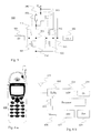
- a level shifting circuit 500 is specially advantageous when implemented in a mobile phone 600 as shown in Figure 6 a.
- the mobile phone 600 may be constructed according to any cellular or cordless standard, including, but not limited to, the Global System for Mobile communications (GSM), the Universal Mobile Telephone System (UMTS), the Digital Enhanced Cordless Telephone (DECT) and the Personal Handyphone System (PHS).
- GSM Global System for Mobile communications
- UMTS Universal Mobile Telephone System
- DECT Digital Enhanced Cordless Telephone
- PHS Personal Handyphone System
- FIG. 6 b shows a block diagram of the mobile phone 600.
- the mobile phone 600 comprises an antenna 631, a transceiver 632, a DSP block 633, a user interface (UI) 634, a processor 635 and a memory 636. It may further comprise a Subscriber Identification Module (SIM) 637 for storing subscriber specific data and/or an auxiliary device 638 integrated in the same casing with or connected to the mobile phone 600.
- SIM Subscriber Identification Module
- a signal such as a speech signal, is received by the mobile phone 600 via the UI 634.
- the signal is processed by the DSP block 633 and is then passed to the transceiver 632.
- the transceiver 632 transmits the signal modulated on a carrier via the antenna 631 to a base station (not shown).
- Downlink signals transmitted by a base station are received by the antenna 631, passed further to the transceiver 632 and processed by the DSP block 633. These signals may then be output by the UI 634.
- the mobile phone 600 is controlled by the processor 635, which is run by an operating code stored in the memory 636.
- the memory 636 may also be used to store other parameters necessary for the mobile phone 600 or the connection to the base station.
- the transceiver 632 is at least partly implemented by digital technology.
- the DSP block 633 may further comprise several circuits each implemented by digital technology. These circuits may use different voltage levels corresponding to logical 1. In cases in which the voltage levels corresponding to logical 1 are differing from each other in these circuits, level shifts are used to connect an output of one such digital circuit to an input of another such digital circuit. This can be done by using a level shifting circuit according to the present invention.
- the transceiver 632 needs high voltages for amplifying the signal to be transmitted to a base station. Part of the blocks shown in Figure 6 b may be using just one, low voltage level corresponding to logical 1. Due to this, the level shifting circuit 500 is implemented as a part of the transceiver 632 in a preferred embodiment of the invention. It is understood by a person skilled in the art that it can equally well be implemented on the same chip with the processor 635, the memory 636 or it can be a further separate element, such as illustrated by the auxiliary device 638.
Landscapes
- Engineering & Computer Science (AREA)
- Computer Hardware Design (AREA)
- Physics & Mathematics (AREA)
- Computing Systems (AREA)
- General Engineering & Computer Science (AREA)
- Mathematical Physics (AREA)
- Logic Circuits (AREA)
Abstract
Description
- The invention relates to a CMOS inverter circuit. It is particularly related to a CMOS based logic level shifting circuit with single operating voltage and low leakage current.
- Digital technology is based on logical ports dealing with binary numbers. Binary numbers only contain zeros and ones, which can be represented by two voltage levels. Logical 0s are represented by a voltage level essentially equal to a set ground level and logical 1s by a voltage level a few volts above the ground level. The voltage level of a logical 1 can be set to any level above the ground level and currently various voltages are used to represent the logical 1 depending on which circuit technology is used.
- As long as all of the circuits of a device are using the same voltage level corresponding to the logical 1s there are no problems. However, in many cases it is necessary to combine units having different voltage levels corresponding to logical 1s. In these cases it is necessary to perform logic level shifting to make the output of one unit suitable as the input to another unit.
- In digital mobile phones the logical ports are generally implemented inside integrated circuits. The design of integrated circuits generally aims at minimising the silicon area occupied and the number of connection pads needed.
- There are several different circuit solutions known in the prior art to perform level shifting. One solution is a
level shifting circuit 100 shown in Figure 1. - In the
level shifting circuit 100, when a voltage at an IN-port 101 is on a level corresponding to logical 1,NMOS transistors ground nodes result PMOS transistors PMOS transistor 114 thus connects an OUT-port 102 to operating voltage VDD. ThePMOS transistors node 133 to be connected to the operating voltage VDD, which again shutsPMOS transistor 115 and prevents current flow through it. - The
level shifting circuit 100 is a circuit for switching the voltage level corresponding to logical 1 at the IN-port 101 to a higher voltage level corresponding to logical 1 at the OUT-port 102. The voltage level corresponding to the logical 1 at the OUT-port 102 is defined by the operating voltage VDD. If the same operating voltage VDD is also applied to PMOS transistor 112 a leakage current problem results. This is illustrated (in connection to Figure 1) by Figure 3, which illustrates voltage-current characteristics of a CMOS inverter 141 (see Figure 1). Gate voltage UG, corresponding to the voltage at anode 134, is shown on the abscissa and drain current ID on the ordinate. When the gate voltage UG is zero the drain current ID is also zero as can be seen by anNMOS curve 301. At the same time thePMOS transistor 112 is in a conducting state, but no current can go through it because it is connected in series with theNMOS transistor 122. As the gate voltage UG starts rising towards the voltage level corresponding to logical 1 the drain current ID can be seen to start rapidly rising until the current starts to be limited by thePMOS transistor 112, as illustrated by aPMOS curve 302, at a breakover point UB. As the gate voltage UG further rises the drain current ID will be reduced to zero again as the gate voltage UG reaches the operating voltage VDD. - However, in a case where an operating voltage V2 of the
CMOS inverter 141 is higher than the voltage level corresponding to logical 1 at the IN-port 101 of thelevel shifting circuit 100, the gate voltage UG never reaches the operating voltage V2. Due to this, there remains a constant leakage current IL through theCMOS inverter 141, which thus increases power consumption of thelevel shifting circuit 100. The leakage current IL is in this case typically in the order of 10 µA. In order to avoid this, theCMOS inverter 141 has the operating voltage V2. The operating voltage V2 is set essentially equal to the voltage level corresponding to logical 1 at the IN-port 101, being thus lower than the operating voltage VDD that is used by all the other parts of thelevel shifting circuit 100. - In the
level shifting circuit 100, when the voltage at the IN-port 101 is on a level corresponding to logical 0,PMOS transistor 111 and thePMOS transistor 112 conduct. As a result thenode 132 is connected to the operating voltage V2.Accordingly NMOS transistor 123 conducts and grounds thenode 133 to cause thePMOS transistor 115 to conduct and connect thenode 131 to the operating voltage VDD through thePMOS transistors NMOS transistor 124 to conduct and to ground the OUT-port 102. At the same, because the voltage at thenode 132 is lower than the operating voltage VDD thePMOS transistor 113 would not be completely shut, if it was connected directly to the operating voltage VDD. However, the gate of thePMOS transistor 116 is connected to the operating voltage VDD through thePMOS transistors PMOS transistor 113. - The
level shifting circuit 100 shown in Figure 1 is complex and requires a large area of silicon on an integrated circuit. It further necessitates one more operating voltage V2 which also demands an extra connection pad to the integrated circuit. The operating voltage V2 is typically obtained from another digital circuit, which makes it very noisy due to all the state changes inside the other digital circuit. - A solution for a
level shifting circuit 200 with one single operating voltage is shown in Figure 2. An IN-port 201side inverter 211 is formed byresistors NMOS transistors current generator 251. An OUT-port 202side CMOS inverter 212 is similar to theCMOS inverter 141 of thelevel shifting circuit 100. - In a typical implementation the values for the
resistors NMOS transistor 232 in the middle of the voltage swing between an operating voltage VDD and the ground potential, thus defining a breakover point UB of theinverter 211. - An NMOS transistor has a channel conductance, which is proportional to the gate-to-source voltage. When a voltage at the IN-
port 201 is on a level corresponding to a logical 0 the channel of theNMOS transistor 231 is completely shut and current flowing through theconstant current generator 251 thus has to completely pass through theNMOS transistor 232. Because no current passes through theresistor 244, the gates ofPMOS transistor 221 andNMOS transistor 233 are connected to the operating voltage VDD. Thus, theNMOS transistor 233 conducts, connecting the OUT-port 202 to ground potential, which is corresponding to logical 0. - When the voltage at the IN-
port 201 is on a level corresponding to logical 1 the channel of theNMOS transistor 231 is completely open and the current flowing through theconstant current generator 251 has to completely pass through theNMOS transistor 231. At the same the gates of thePMOS transistor 221 and theNMOS transistor 233 are grounded, causing thePMOS transistor 221 to conduct, connecting the OUT-port 202 to the operating voltage VDD, which is corresponding to logical 1. - The level shifting
circuit 200 only needs one operating voltage VDD, but the construction is still complicated and further has a problem of leakage current. The leakage current of thelevel shifting circuit 200 through the constantcurrent generator 251 is typically in the order of 5 to 10 µA. - A straightforward solution for level shifting would be to provide a
buffer circuit 400 as shown in Figure 4. Thebuffer circuit 400 comprises two CMOS inverters, afirst CMOS inverter 411 comprisingPMOS transistor 421 andNMOS transistor 431 and asecond CMOS inverter 412 being formed byPMOS transistor 422 andNMOS transistor 432. Both of theCMOS inverters - When a voltage at an IN-
port 401 is corresponding to logical 1, theNMOS transistor 431 conducts, thus grounding anode 441. As a result thePMOS transistor 422 conducts and an OUT-port 402 is connected to the operating voltage VDD. If the voltage level corresponding to logical 1 level at the IN-port 401 is 2 volts and the operating voltage VDD is 3 volts, a shift from a logical 1 level of 2 volts to a logical 1 level of 3 volts is carried out. However, because the voltage at the IN-port 401 does not reach the operating voltage VDD there remains a leakage current IL through theCMOS inverter 411. - When the IN-
port 401 is connected to the voltage level corresponding to logical 0 thePMOS transistor 421 conducts. Thenode 441 is thus connected to the operating voltage VDD. As a result, theNMOS transistor 432 conducts and connects the OUT-port 402 to a ground potential. - The
buffer circuit 400 is not used for level shifting because of a serious problem of leakage current in the event that the voltage level corresponding to logical 1 at the IN-port 401 side of thebuffer circuit 400 is lower than the operating voltage VDD - Accordingly, there is clearly a need for a simple, low leakage level shifting circuit that is operated by a single operating voltage.
- According to a first aspect of the invention there is provided a level shifting circuit for shifting a first voltage level to a second voltage level comprising a first inverter and a second inverter, an output of the first inverter being connected to an input of the second inverter, an input of the first inverter forming an input port of the level shifting circuit for inputting the first voltage level and an output of the second inverter forming an output port of the level shifting circuit for the second voltage level, the level shifting circuit being operated by a single operating voltage characterised in that the level shifting circuit further comprises a leakage current limiting circuit connected in series between the first inverter and the operating voltage for limiting a leakage current through the logic level shifting circuit in a situation when the first voltage level is below the operating voltage.
- The level shifting circuit is preferably used for shifting logical levels, the first voltage level corresponding to a first logical 1 in a first digital circuit and the second voltage level corresponding to a second logical 1 in a second digital circuit. In a preferred embodiment of the present invention the operating voltage corresponds to the second voltage level. In another preferred embodiment at least one of the first and the second inverters is implemented by CMOS technology. The leakage current limiting circuit preferably comprises a PMOS transistor and a resistor by-passing the channel of the PMOS transistor. Preferably the resistor value is set to a value that does not substantially slow down the operation of the logic level shifting circuit. In a yet further preferred embodiment the resistor value is chosen from a range between 100 kΩ and 1 MΩ.
- In a second aspect of the invention there is provided a digital logic circuitry comprising a plurality of subcircuits, each subcircuit using one of a plurality of voltage levels, a first voltage level of the plurality of voltage levels differing from a second voltage level of the plurality of voltage levels, a first subcircuit of the plurality of subcircuits being a level shifting circuit for shifting the first voltage level output from a second subcircuit of the plurality of subcircuits to the second voltage level for inputting to a third subcircuit of the plurality of subcircuits, the first subcircuit comprising a first inverter and a second inverter, an output of the first inverter being connected to an input of the second inverter, an input of the first inverter forming an input port of the first subcircuit for inputting the first voltage level and an output of the second inverter forming an output port of the first subcircuit for outputting the second voltage level, the first subcircuit being operated by a single operating voltage characterised in that the first subcircuit further comprises a leakage current limiting circuit connected in series between the first inverter and the operating voltage for limiting a leakage current through the first subcircuit in a situation when the first voltage level is below the operating voltage.
- Preferably the second subcircuit is a digital logic circuit, in which the first voltage level is corresponding to a first logical 1, and the third subcircuit is another digital logic circuit, in which the second voltage level is corresponding to a second logical 1. In a preferred embodiment the operating voltage is corresponding to the second voltage level. In another preferred embodiment at least one of the first and the second inverters is implemented by CMOS technology. The leakage current limiting circuit preferably comprises a PMOS transistor and a resistor by-passing the channel of the PMOS transistor. Preferably the resistor value is set to a value that does not substantially slow down the operation of the first subcircuit. In a yet further preferred embodiment the resistor value is chosen from a range between 100 kΩ and 1 MΩ.
- In a third aspect of the invention there is provided a mobile phone comprising a level shifting circuit for shifting a first voltage level, output from a first digital circuit, to a second voltage level for inputting to a second digital circuit, the level shifting circuit comprising a first inverter and a second inverter, an output of the first inverter being connected to an input of the second inverter, an input of the first inverter forming an input port of the level shifting circuit for inputting the first voltage level and an output of the second inverter forming an output port of the level shifting circuit for outputting the second voltage level, the level shifting circuit being operated by a single operating voltage characterised in that the level shifting circuit further comprises a leakage current limiting circuit connected in series between the first inverter and the operating voltage for limiting a leakage current through the logic level shifting circuit in a situation when the first voltage level is below the operating voltage.
- The level shifting circuit is preferably used for shifting logical levels, the first voltage level corresponding to a first logical 1 and the second voltage level corresponding to a second logical 1. Preferably the first digital circuit and the second digital circuit are logical circuits handling binary data. In a preferred embodiment the operating voltage is corresponding to the second voltage level. In another preferred embodiment at least one of the first and the second inverters is implemented by CMOS technology. The leakage current limiting circuit preferably comprises a PMOS transistor and a resistor by-passing the channel of the PMOS transistor. Preferably the resistor value is set to a value that does not substantially slow down the operation of the logic level shifting circuit. In a yet further preferred embodiment the resistor value is chosen from a range between 100 kΩ and 1 MΩ.
- The invention will be described by way of example only with reference to the accompanying drawings, in which:
- Figure 1 shows a circuit known in the prior art for performing a logical level shift with two operating voltages;
- Figure 2 shows a solution for performing a logical level shift with a single operating voltage;
- Figure 3 shows a typical UI curve of a CMOS circuit;
- Figure 4 shows a simple solution for performing a logical level shift with a single operating voltage using a buffer circuit;
- Figure 5 shows a logical level shifting circuit according to the present invention;
- Figure 6 a shows a mobile phone incorporating a logical level shifting circuit according to the present invention; and
- Figure 6 b shows a simplified block diagram of a mobile phone incorporating a logical level shifting circuit according to the present invention.
-
- A
level shifting circuit 500 according to the present invention is shown in Figure 5. Thelevel shifting circuit 500 comprises afirst CMOS inverter 542 and asecond CMOS inverter 543. Thefirst CMOS inverter 542 and thesecond CMOS inverter 543 each comprise aPMOS transistor NMOS transistor PMOS transistor NMOS transistor respective CMOS inverter PMOS transistor NMOS transistor 521, forming an output of therespective CMOS inverter node 551 is shown as the output of thefirst CMOS inverter 542. Thenode 551 is connected to the input of thesecond CMOS inverter 543. Thus, a cascade connection is formed between thefirst CMOS inverters 542 and thesecond CMOS inverter 543. An IN-port 501 works as the 500. Respectively, an OUT-port 502 works as the output of thesecond CMOS inverter 543 and as an output of thelevel shifting circuit 500. Thelevel shifting circuit 500 further comprises a leakage current limitingcircuit 541 comprising aPMOS transistor 513 and aresistor 531 connected in parallel between the drain and the source of thePMOS transistor 513. The source of thePMOS transistor 513 is connected to operating voltage VDD (via a voltage supply point) and the drain of thePMOS transistor 513 is connected to the source of thePMOS transistor 511. - An example of operation of the
level shifting circuit 500 is now described. The IN-port 501 is connected to a voltage level of 2 V corresponding to logical 1 at the IN-port 501 side of thelevel shifting circuit 500. The operating voltage VDD is 3V corresponding to logical 1 level at the OUT-port 502 side of thelevel shifting circuit 500. A positive gate-to-source voltage causes theNMOS transistor 521 to conduct and thus to connect thenode 551 to ground potential. As a result the gates of theNMOS transistor 522 and thePMOS transistor 512 are grounded due to which theNMOS transistor 522 is closed and thePMOS transistor 512 conducts. ThePMOS transistor 512 thus connects the OUT-port 502 to the operating voltage VDD (via the voltage supply point). At the same, the operating voltage VDD is also applied to the gate of thePMOS transistor 513, thus keeping thePMOS transistor 513 in nonconductive state. Hence, there is a leakage current IL flowing from the operating voltage VDD through theresistor 531, thePMOS transistor 511 and theNMOS transistor 521 to the ground potential because of thePMOS transistor 511 not completely closing due to the gate voltage still being lower than the operating voltage VDD. This leakage current IL, however, will be limited to a small value by theresistor 531. - The value for the
resistor 531 is high in order to limit the leakage current IL. Setting the value to infinity, for example, by deleting theresistor 531 completely from the circuit diagram of thelevel shifting circuit 500, would set the leakage current IL to zero. However, this would make thelevel shifting circuit 500 inoperable in the case where the voltage at the IN-port 501 goes from the voltage corresponding to logical 1 to the voltage corresponding to logical 0. - Let us now consider the case where the IN-
port 501 is set to the voltage corresponding to logical 0. Grounding the gates of thePMOS transistor 511 and theNMOS transistor 521 causes theNMOS transistor 521 to be closed and thePMOS transistor 511 to be in a conductive state. Thenode 551 is then connected to the operating voltage VDD through theresistor 531. Because no current passes through the gates of thePMOS transistor 512 and theNMOS transistor 522 the limited current flowing through theresistor 531 is enough to cause the voltage of thenode 551 rapidly to exceed a breakover point UB of thesecond CMOS inverter 543 after which theNMOS transistor 522 conducts and grounds the OUT-port 502. At the same time the gate of thePMOS transistor 513 is also grounded causing thePMOS transistor 513 to conduct and thus to connect thenode 551 to the operating voltage VDD. - It is clearly seen that setting the value of the
resistor 531 to infinity would block the function of thelevel shifting circuit 500, since a transition from the voltage level corresponding to logical 1 to the voltage level corresponding to logical 0 at the IN-port 501 would not cause any change at the OUT-port 502. Instead, the OUT-port 502 would constantly remain on a voltage level corresponding to logical 1. Setting the value of theresistor 531 too high would make thelevel shifting circuit 500 function very slowly. On the other hand, a value, which is too low, would not limit the leakage current in the case in which the IN-port 501 is on the voltage level corresponding to logical 1. There is clearly an optimal range for the value of theresistor 531. In a preferred embodiment of the present invention the value for theresistor 531 is set to 500 kΩ. - A
level shifting circuit 500 is specially advantageous when implemented in amobile phone 600 as shown in Figure 6 a. Themobile phone 600 may be constructed according to any cellular or cordless standard, including, but not limited to, the Global System for Mobile communications (GSM), the Universal Mobile Telephone System (UMTS), the Digital Enhanced Cordless Telephone (DECT) and the Personal Handyphone System (PHS). - Figure 6 b shows a block diagram of the
mobile phone 600. Themobile phone 600 comprises anantenna 631, atransceiver 632, aDSP block 633, a user interface (UI) 634, aprocessor 635 and amemory 636. It may further comprise a Subscriber Identification Module (SIM) 637 for storing subscriber specific data and/or anauxiliary device 638 integrated in the same casing with or connected to themobile phone 600. A signal, such as a speech signal, is received by themobile phone 600 via theUI 634. The signal is processed by theDSP block 633 and is then passed to thetransceiver 632. Thetransceiver 632 transmits the signal modulated on a carrier via theantenna 631 to a base station (not shown). Downlink signals transmitted by a base station (not shown) are received by theantenna 631, passed further to thetransceiver 632 and processed by theDSP block 633. These signals may then be output by theUI 634. Themobile phone 600 is controlled by theprocessor 635, which is run by an operating code stored in thememory 636. Thememory 636 may also be used to store other parameters necessary for themobile phone 600 or the connection to the base station. - In most modern mobile phones besides the
processor 635, thememory 636 and theDSP block 633, also thetransceiver 632 is at least partly implemented by digital technology. TheDSP block 633 may further comprise several circuits each implemented by digital technology. These circuits may use different voltage levels corresponding to logical 1. In cases in which the voltage levels corresponding to logical 1 are differing from each other in these circuits, level shifts are used to connect an output of one such digital circuit to an input of another such digital circuit. This can be done by using a level shifting circuit according to the present invention. - The
transceiver 632 needs high voltages for amplifying the signal to be transmitted to a base station. Part of the blocks shown in Figure 6 b may be using just one, low voltage level corresponding to logical 1. Due to this, thelevel shifting circuit 500 is implemented as a part of thetransceiver 632 in a preferred embodiment of the invention. It is understood by a person skilled in the art that it can equally well be implemented on the same chip with theprocessor 635, thememory 636 or it can be a further separate element, such as illustrated by theauxiliary device 638. - Although described in the context of presently preferred embodiments, it should be noted that a number of modifications to these teachings may occur to the person skilled in the art. It will thus be understood by the persons skilled in the art that even though the invention has been shown and described with respect to preferred embodiments thereof, several changes may be made therein without departing from the scope and the spirit of the invention. These changes and modifications, which are clear to those skilled in the art, are intended to be included within the scope of the present invention as defined by the enclosed claims.
Claims (24)
- A level shifting circuit for shifting a first voltage level to a second voltage level comprising a first inverter and a second inverter, an output of the first inverter being connected to an input of the second inverter, an input of the first inverter forming an input port of the level shifting circuit for inputting the first voltage level and an output of the second inverter forming an output port of the level shifting circuit for outputting the second voltage level, a voltage supply point via which the level shifting circuit is supplied with an operating voltage characterised in that the level shifting circuit further comprises a leakage current limiting circuit connected in series between the first inverter and the voltage supply point for limiting a leakage current through the logic level shifting circuit.
- A level shifting circuit according to claim 1, characterised in that the first voltage level is corresponding to a first logical 1 in a first digital circuit and the second voltage level is corresponding to a second logical 1 in a second digital circuit.
- A level shifting circuit according to claim 1 or claim 2, characterised in that the second voltage level corresponds to the operating voltage.
- A level shifting circuit according to any one of the preceding claims, characterised in that at least one of the first inverter and the second inverter is implemented using CMOS technology.
- A level shifting circuit according to any one of the preceding claims, characterised in that at least one of the first inverter and the second inverter comprises a PMOS transistor and an NMOS transistor, the gate of the PMOS transistor being connected to the gate of the NMOS transistor forming the input of the inverter and the drain of the PMOS transistor being connected to the drain of the NMOS transistor forming the output of the inverter.
- A level shifting circuit according to any one of the preceding claims, characterised in that the leakage current limiting circuit comprises a PMOS transistor the drain of the PMOS transistor being connected to the first inverter, the source of the PMOS transistor being connected to the operating voltage, the gate of the PMOS transistor being connected to the output of the level shifting circuit and a resistor being connected between the drain of the PMOS transistor and the source of the PMOS transistor to allow a limited current flow from the operating voltage to the first CMOS inverter in a situation when the channel of the PMOS transistor is shut.
- A level shifting circuit according to claim 6, characterised in that the resistor value is set so as not substantially to slow down the function of the level shifting circuit.
- A level shifting circuit according to claim 6 or claim 7 characterised in that the resistor has a value in a range between 100 kΩ and 1 MΩ.
- A digital logic circuitry comprising a plurality of subcircuits, each subcircuit using one of a plurality of voltage levels, a first voltage level of the plurality of voltage levels differing from a second voltage level of the plurality of voltage levels, a first subcircuit of the plurality of subcircuits being a level shifting circuit for shifting the first voltage level output from a second subcircuit of the plurality of subcircuits to the second voltage level for inputting to a third subcircuit of the plurality of subcircuits, the first subcircuit comprising a first inverter and a second inverter, an output of the first inverter being connected to an input of the second inverter, an input of the first inverter forming an input port of the first subcircuit for inputting the first voltage level and an output of the second inverter forming an output port of the first subcircuit for outputting the second voltage level, a voltage supply point via which the first subcircuit is supplied with an operating voltage characterised in that the first subcircuit further comprises a leakage current limiting circuit connected in series between the first inverter and the voltage supply point for limiting a leakage current through the first subcircuit.
- A digital logic circuitry according to claim 9, characterised in that the first voltage level is corresponding to a first logical 1 in the second subcircuit and the second voltage level is corresponding to a second logical 1 in the third subcircuit.
- A digital logic circuitry according to claim 9 or claim 10, characterised in that the second voltage level corresponds to the operating voltage.
- A digital logic circuitry according to any one of the preceding claims 9 to 11, characterised in that at least one of the first inverter and the second inverter is implemented using CMOS technology.
- A digital logic circuitry according to any one of the preceding claims 9 to 12, characterised in that at least one of the first inverter and the second inverter comprises a PMOS transistor and an NMOS transistor, the gate of the PMOS transistor being connected to the gate of the NMOS transistor forming the input of the inverter and the drain of the PMOS transistor being connected to the drain of the NMOS transistor forming the output of the inverter.
- A digital logic circuitry according to any one of the preceding claims 9 to 13, characterised in that the leakage current limiting circuit comprises a PMOS transistor the drain of the PMOS transistor being connected to the first inverter, the source of the PMOS transistor being connected to the operating voltage, the gate of the PMOS transistor being connected to the output of the second subcircuit and a resistor being connected between the drain of the PMOS transistor and the source of the PMOS transistor to allow a limited current flow from the operating voltage to the first inverter in a situation when the channel of the PMOS transistor is shut.
- A digital logic circuitry according to claim 14, characterised in that the resistor value is set so as not substantially to slow down the function of the logic level shifting circuit.
- A digital logic circuitry according to claim 14 or claim 15, characterised in that the resistor has a value in a range between 100 kΩ and 1 MΩ.
- A mobile phone comprising a level shifting circuit for shifting a first voltage level, output from a first digital circuit, to a second voltage level for inputting to a second digital circuit, the level shifting circuit comprising a first inverter and a second inverter, an output of the first inverter being connected to an input of the second inverter, an input of the first inverter forming an input port of the level shifting circuit for inputting the first voltage level and an output of the second inverter forming an output port of the level shifting circuit for outputting the second voltage level, a voltage supply point via which the level shifting circuit is supplied with an operating voltage characterised in that the level shifting circuit further comprises a leakage current limiting circuit connected in series between the first inverter and the voltage supply point for limiting a leakage current through the logic level shifting circuit.
- A mobile phone according to claim 17, characterised in that the first voltage level is corresponding to a first logical 1 in a first digital circuit and the second voltage level is corresponding to a second logical 1 in a second digital circuit.
- A mobile phone according to claim 17 or claim 18, characterised in that the second voltage level corresponds to the operating voltage.
- A mobile phone according to any one of the preceding claims 17 to 19, characterised in that at least one of the first inverter and the second inverter is implemented using CMOS technology.
- A mobile phone according to any one of the preceding claims 17 to 20, characterised in that at least one of the first inverter and the second inverter comprises a PMOS transistor and an NMOS transistor, the gate of the PMOS transistor being connected to the gate of the NMOS transistor forming the input of the inverter and the drain of the PMOS transistor being connected to the drain of the NMOS transistor forming the output of the inverter.
- A mobile phone according to any one of the preceding claims 17 to 21, characterised in that the leakage current limiting circuit comprises a PMOS transistor the drain of the PMOS transistor being connected to the first inverter, the source of the PMOS transistor being connected to the operating voltage, the gate of the PMOS transistor being connected to the output of the second subcircuit and a resistor being connected between the drain of the PMOS transistor and the source of the PMOS transistor to allow a limited current flow from the operating voltage to the first inverter in a situation when the channel of the PMOS transistor is shut.
- A mobile phone according to claim 22, characterised in that the resistor value is set so as not substantially to slow down the function of the logic level shifting circuit.
- A mobile phone according to claim 22 or claim 23, characterised in that the resistor has a value in a range between 100 kΩ and 1 MΩ.
Applications Claiming Priority (2)
| Application Number | Priority Date | Filing Date | Title |
|---|---|---|---|
| FI20010404 | 2001-02-28 | ||
| FI20010404A FI20010404A0 (en) | 2001-02-28 | 2001-02-28 | Logic level switching circuit |
Publications (1)
| Publication Number | Publication Date |
|---|---|
| EP1237278A1 true EP1237278A1 (en) | 2002-09-04 |
Family
ID=8560572
Family Applications (1)
| Application Number | Title | Priority Date | Filing Date |
|---|---|---|---|
| EP02396014A Withdrawn EP1237278A1 (en) | 2001-02-28 | 2002-02-07 | Logic level shifting circuit |
Country Status (3)
| Country | Link |
|---|---|
| US (1) | US20020118040A1 (en) |
| EP (1) | EP1237278A1 (en) |
| FI (1) | FI20010404A0 (en) |
Cited By (4)
| Publication number | Priority date | Publication date | Assignee | Title |
|---|---|---|---|---|
| WO2006103624A1 (en) * | 2005-03-31 | 2006-10-05 | Nxp B.V. | Electronic device |
| WO2021263277A1 (en) * | 2020-06-24 | 2021-12-30 | Microchip Technology Incorporated | Recognizing transistor-transistor logic levels (ttl) at an input circuit with increased immunity to static current draw |
| US11742005B2 (en) | 2021-03-08 | 2023-08-29 | Microchip Technology Incorporated | Selectively cross-coupled inverters, and related devices, systems, and methods |
| US12298927B2 (en) | 2019-06-27 | 2025-05-13 | Microchip Technology Incorporated | Selectable input buffers of general purpose inputs and microcontrollers having the same |
Families Citing this family (5)
| Publication number | Priority date | Publication date | Assignee | Title |
|---|---|---|---|---|
| JP3730963B2 (en) * | 2003-01-21 | 2006-01-05 | 沖電気工業株式会社 | Semiconductor integrated circuit |
| KR20110011988A (en) * | 2009-07-29 | 2011-02-09 | 삼성전자주식회사 | Level shifter and display device using same |
| DE102011084985A1 (en) * | 2010-11-12 | 2012-05-16 | Samsung Electronics Co., Ltd. | Level shifter and system-on-chip and multimedia device with selbigem |
| CN112904122B (en) * | 2021-01-22 | 2024-09-20 | 维沃移动通信有限公司 | Insertion detection circuit and electronic equipment |
| CN114389598A (en) * | 2022-03-23 | 2022-04-22 | 武汉市聚芯微电子有限责任公司 | Conversion device, interface circuit and chip |
Citations (6)
| Publication number | Priority date | Publication date | Assignee | Title |
|---|---|---|---|---|
| US5087841A (en) * | 1990-04-09 | 1992-02-11 | National Semiconductor Corporation | TTL to CMOS translating circuits without static current |
| EP0546702A1 (en) * | 1991-12-12 | 1993-06-16 | AT&T Corp. | CMOS input buffer with high speed and low power |
| EP0621694A2 (en) * | 1993-04-20 | 1994-10-26 | International Business Machines Corporation | Low power interface circuit |
| US5565795A (en) * | 1994-08-16 | 1996-10-15 | Oki Electric Industry Co., Ltd. | Level converting circuit for reducing an on-quiescence current |
| DE19719448A1 (en) * | 1997-05-07 | 1998-11-12 | Siemens Ag | Inverter circuit for level converter |
| US5955893A (en) * | 1996-12-16 | 1999-09-21 | Macronix International Co., Ltd. | Power saving buffer circuit buffer bias voltages |
-
2001
- 2001-02-28 FI FI20010404A patent/FI20010404A0/en unknown
-
2002
- 2002-02-07 EP EP02396014A patent/EP1237278A1/en not_active Withdrawn
- 2002-02-12 US US10/074,079 patent/US20020118040A1/en not_active Abandoned
Patent Citations (6)
| Publication number | Priority date | Publication date | Assignee | Title |
|---|---|---|---|---|
| US5087841A (en) * | 1990-04-09 | 1992-02-11 | National Semiconductor Corporation | TTL to CMOS translating circuits without static current |
| EP0546702A1 (en) * | 1991-12-12 | 1993-06-16 | AT&T Corp. | CMOS input buffer with high speed and low power |
| EP0621694A2 (en) * | 1993-04-20 | 1994-10-26 | International Business Machines Corporation | Low power interface circuit |
| US5565795A (en) * | 1994-08-16 | 1996-10-15 | Oki Electric Industry Co., Ltd. | Level converting circuit for reducing an on-quiescence current |
| US5955893A (en) * | 1996-12-16 | 1999-09-21 | Macronix International Co., Ltd. | Power saving buffer circuit buffer bias voltages |
| DE19719448A1 (en) * | 1997-05-07 | 1998-11-12 | Siemens Ag | Inverter circuit for level converter |
Cited By (5)
| Publication number | Priority date | Publication date | Assignee | Title |
|---|---|---|---|---|
| WO2006103624A1 (en) * | 2005-03-31 | 2006-10-05 | Nxp B.V. | Electronic device |
| US12298927B2 (en) | 2019-06-27 | 2025-05-13 | Microchip Technology Incorporated | Selectable input buffers of general purpose inputs and microcontrollers having the same |
| WO2021263277A1 (en) * | 2020-06-24 | 2021-12-30 | Microchip Technology Incorporated | Recognizing transistor-transistor logic levels (ttl) at an input circuit with increased immunity to static current draw |
| US12052016B2 (en) | 2020-06-24 | 2024-07-30 | Microchip Technology Corporation | Recognizing transistor-transistor logic levels (TTL) at an input circuit with increased immunity to static current draw |
| US11742005B2 (en) | 2021-03-08 | 2023-08-29 | Microchip Technology Incorporated | Selectively cross-coupled inverters, and related devices, systems, and methods |
Also Published As
| Publication number | Publication date |
|---|---|
| FI20010404A0 (en) | 2001-02-28 |
| US20020118040A1 (en) | 2002-08-29 |
Similar Documents
| Publication | Publication Date | Title |
|---|---|---|
| US8965304B2 (en) | Multi-mode I/O circuitry supporting low interference signaling schemes for high speed digital interfaces | |
| US6060910A (en) | Dynamic logic circuit | |
| US6856173B1 (en) | Multiplexing of digital signals at multiple supply voltages in an integrated circuit | |
| US6838924B1 (en) | Dual stage level shifter for low voltage operation | |
| US20020053923A1 (en) | Programmable termination circuit and method | |
| EP0621694B1 (en) | Low power interface circuit | |
| US5886556A (en) | Low power schmitt trigger | |
| US4996453A (en) | Power down circuit for low-power circuit with dual supply voltages | |
| US5047663A (en) | Low-power comparator which tolerates high-slew-rate incoming signals and deriving power from the incoming signals | |
| US20020118040A1 (en) | Logic level shifting circuit | |
| US5032742A (en) | ESD circuit for input which exceeds power supplies in normal operation | |
| EP1304842B1 (en) | Serial differential data link with automatic power down | |
| US20040095175A1 (en) | Flip-flop circuit with reduced power consumption | |
| EP1537666A2 (en) | Supply voltage modulation circuit for mos transistors, reconfigurable logic device and method of processing an input signal to a logic circuit | |
| KR100446303B1 (en) | Clocked-scan flip-flop for multi-threshold voltage CMOS circuit | |
| EP0450453B1 (en) | BICMOS input circuit for detecting signals out of ECL range | |
| EP1369762A1 (en) | Active subscriber information module | |
| US6225830B1 (en) | Differential mode logic gate having NAND and NOR portions to produce complementary outputs | |
| US6798267B1 (en) | Buffer circuit with programmable switching thresholds | |
| US5003362A (en) | Integrated circuit with high-impedance well tie | |
| JP4115973B2 (en) | Semiconductor device and control method | |
| US6429691B1 (en) | Differential-input circuit | |
| US5955924A (en) | Differential metal-oxide semiconductor (CMOS) push-pull buffer | |
| JP3923397B2 (en) | Level translator circuit | |
| US5025177A (en) | Sensitive low power comparator |
Legal Events
| Date | Code | Title | Description |
|---|---|---|---|
| PUAI | Public reference made under article 153(3) epc to a published international application that has entered the european phase |
Free format text: ORIGINAL CODE: 0009012 |
|
| AK | Designated contracting states |
Kind code of ref document: A1 Designated state(s): AT BE CH CY DE DK ES FI FR GB GR IE IT LI LU MC NL PT SE TR |
|
| AX | Request for extension of the european patent |
Free format text: AL;LT;LV;MK;RO;SI |
|
| 17P | Request for examination filed |
Effective date: 20030304 |
|
| AKX | Designation fees paid |
Designated state(s): AT BE CH CY DE DK ES FI FR GB GR IE IT LI LU MC NL PT SE TR |
|
| 17Q | First examination report despatched |
Effective date: 20041126 |
|
| STAA | Information on the status of an ep patent application or granted ep patent |
Free format text: STATUS: THE APPLICATION IS DEEMED TO BE WITHDRAWN |
|
| 18D | Application deemed to be withdrawn |
Effective date: 20050607 |