EP1238708B1 - Tintenstrahldrucker und herstellung eines substrats mit einer funktionellen flüssigkeit - Google Patents
Tintenstrahldrucker und herstellung eines substrats mit einer funktionellen flüssigkeit Download PDFInfo
- Publication number
- EP1238708B1 EP1238708B1 EP01976714A EP01976714A EP1238708B1 EP 1238708 B1 EP1238708 B1 EP 1238708B1 EP 01976714 A EP01976714 A EP 01976714A EP 01976714 A EP01976714 A EP 01976714A EP 1238708 B1 EP1238708 B1 EP 1238708B1
- Authority
- EP
- European Patent Office
- Prior art keywords
- nozzles
- waveform
- functional liquid
- supply port
- ink jet
- Prior art date
- Legal status (The legal status is an assumption and is not a legal conclusion. Google has not performed a legal analysis and makes no representation as to the accuracy of the status listed.)
- Expired - Lifetime
Links
- 239000007788 liquid Substances 0.000 title claims abstract description 67
- 239000000758 substrate Substances 0.000 title claims abstract description 61
- 238000004519 manufacturing process Methods 0.000 title claims abstract description 29
- 238000000034 method Methods 0.000 claims abstract description 22
- 238000007599 discharging Methods 0.000 claims abstract description 10
- 230000001105 regulatory effect Effects 0.000 claims description 5
- 239000000976 ink Substances 0.000 description 113
- 239000004973 liquid crystal related substance Substances 0.000 description 17
- 239000010408 film Substances 0.000 description 13
- 230000001276 controlling effect Effects 0.000 description 10
- 238000010586 diagram Methods 0.000 description 10
- 238000005192 partition Methods 0.000 description 9
- 230000007246 mechanism Effects 0.000 description 8
- 238000004040 coloring Methods 0.000 description 7
- 238000004140 cleaning Methods 0.000 description 6
- 239000011159 matrix material Substances 0.000 description 6
- 230000000903 blocking effect Effects 0.000 description 5
- 238000001035 drying Methods 0.000 description 5
- 238000005530 etching Methods 0.000 description 5
- 230000015572 biosynthetic process Effects 0.000 description 4
- 239000000463 material Substances 0.000 description 4
- 239000004065 semiconductor Substances 0.000 description 4
- KDLHZDBZIXYQEI-UHFFFAOYSA-N Palladium Chemical compound [Pd] KDLHZDBZIXYQEI-UHFFFAOYSA-N 0.000 description 3
- KWYUFKZDYYNOTN-UHFFFAOYSA-M Potassium hydroxide Chemical compound [OH-].[K+] KWYUFKZDYYNOTN-UHFFFAOYSA-M 0.000 description 3
- 239000003086 colorant Substances 0.000 description 3
- 230000012447 hatching Effects 0.000 description 3
- 239000002184 metal Substances 0.000 description 3
- 229910052751 metal Inorganic materials 0.000 description 3
- 239000000203 mixture Substances 0.000 description 3
- BASFCYQUMIYNBI-UHFFFAOYSA-N platinum Chemical compound [Pt] BASFCYQUMIYNBI-UHFFFAOYSA-N 0.000 description 3
- 239000002904 solvent Substances 0.000 description 3
- 102000053602 DNA Human genes 0.000 description 2
- 108020004414 DNA Proteins 0.000 description 2
- VEXZGXHMUGYJMC-UHFFFAOYSA-N Hydrochloric acid Chemical compound Cl VEXZGXHMUGYJMC-UHFFFAOYSA-N 0.000 description 2
- MHAJPDPJQMAIIY-UHFFFAOYSA-N Hydrogen peroxide Chemical compound OO MHAJPDPJQMAIIY-UHFFFAOYSA-N 0.000 description 2
- 238000009835 boiling Methods 0.000 description 2
- 239000003054 catalyst Substances 0.000 description 2
- 239000011248 coating agent Substances 0.000 description 2
- 238000000576 coating method Methods 0.000 description 2
- 239000010949 copper Substances 0.000 description 2
- JHIVVAPYMSGYDF-UHFFFAOYSA-N cyclohexanone Chemical compound O=C1CCCCC1 JHIVVAPYMSGYDF-UHFFFAOYSA-N 0.000 description 2
- 239000002270 dispersing agent Substances 0.000 description 2
- 239000006185 dispersion Substances 0.000 description 2
- 238000009826 distribution Methods 0.000 description 2
- 230000000694 effects Effects 0.000 description 2
- 239000011521 glass Substances 0.000 description 2
- 239000010931 gold Substances 0.000 description 2
- 238000010438 heat treatment Methods 0.000 description 2
- 230000005499 meniscus Effects 0.000 description 2
- 239000002245 particle Substances 0.000 description 2
- 229920002120 photoresistant polymer Polymers 0.000 description 2
- 239000000843 powder Substances 0.000 description 2
- 239000010970 precious metal Substances 0.000 description 2
- 229920005989 resin Polymers 0.000 description 2
- 239000011347 resin Substances 0.000 description 2
- XLYOFNOQVPJJNP-UHFFFAOYSA-N water Substances O XLYOFNOQVPJJNP-UHFFFAOYSA-N 0.000 description 2
- VXQBJTKSVGFQOL-UHFFFAOYSA-N 2-(2-butoxyethoxy)ethyl acetate Chemical compound CCCCOCCOCCOC(C)=O VXQBJTKSVGFQOL-UHFFFAOYSA-N 0.000 description 1
- 239000004925 Acrylic resin Substances 0.000 description 1
- 229920000178 Acrylic resin Polymers 0.000 description 1
- DKPFZGUDAPQIHT-UHFFFAOYSA-N Butyl acetate Natural products CCCCOC(C)=O DKPFZGUDAPQIHT-UHFFFAOYSA-N 0.000 description 1
- OKTJSMMVPCPJKN-UHFFFAOYSA-N Carbon Chemical compound [C] OKTJSMMVPCPJKN-UHFFFAOYSA-N 0.000 description 1
- VYZAMTAEIAYCRO-UHFFFAOYSA-N Chromium Chemical compound [Cr] VYZAMTAEIAYCRO-UHFFFAOYSA-N 0.000 description 1
- RYGMFSIKBFXOCR-UHFFFAOYSA-N Copper Chemical compound [Cu] RYGMFSIKBFXOCR-UHFFFAOYSA-N 0.000 description 1
- BQCADISMDOOEFD-UHFFFAOYSA-N Silver Chemical compound [Ag] BQCADISMDOOEFD-UHFFFAOYSA-N 0.000 description 1
- NIXOWILDQLNWCW-UHFFFAOYSA-N acrylic acid group Chemical group C(C=C)(=O)O NIXOWILDQLNWCW-UHFFFAOYSA-N 0.000 description 1
- QVGXLLKOCUKJST-UHFFFAOYSA-N atomic oxygen Chemical compound [O] QVGXLLKOCUKJST-UHFFFAOYSA-N 0.000 description 1
- 239000011230 binding agent Substances 0.000 description 1
- 239000002041 carbon nanotube Substances 0.000 description 1
- 229910021393 carbon nanotube Inorganic materials 0.000 description 1
- 229910052804 chromium Inorganic materials 0.000 description 1
- 239000011651 chromium Substances 0.000 description 1
- 229920001940 conductive polymer Polymers 0.000 description 1
- 229910052802 copper Inorganic materials 0.000 description 1
- 238000001312 dry etching Methods 0.000 description 1
- 230000005684 electric field Effects 0.000 description 1
- 238000005401 electroluminescence Methods 0.000 description 1
- 239000000446 fuel Substances 0.000 description 1
- 230000006870 function Effects 0.000 description 1
- 239000007789 gas Substances 0.000 description 1
- 230000007274 generation of a signal involved in cell-cell signaling Effects 0.000 description 1
- 238000012252 genetic analysis Methods 0.000 description 1
- PCHJSUWPFVWCPO-UHFFFAOYSA-N gold Chemical compound [Au] PCHJSUWPFVWCPO-UHFFFAOYSA-N 0.000 description 1
- 229910052737 gold Inorganic materials 0.000 description 1
- 239000001307 helium Substances 0.000 description 1
- 229910052734 helium Inorganic materials 0.000 description 1
- SWQJXJOGLNCZEY-UHFFFAOYSA-N helium atom Chemical compound [He] SWQJXJOGLNCZEY-UHFFFAOYSA-N 0.000 description 1
- FUZZWVXGSFPDMH-UHFFFAOYSA-N hexanoic acid Chemical compound CCCCCC(O)=O FUZZWVXGSFPDMH-UHFFFAOYSA-N 0.000 description 1
- AMGQUBHHOARCQH-UHFFFAOYSA-N indium;oxotin Chemical compound [In].[Sn]=O AMGQUBHHOARCQH-UHFFFAOYSA-N 0.000 description 1
- 230000006698 induction Effects 0.000 description 1
- 230000010365 information processing Effects 0.000 description 1
- 239000001023 inorganic pigment Substances 0.000 description 1
- 238000005259 measurement Methods 0.000 description 1
- 239000002736 nonionic surfactant Substances 0.000 description 1
- 230000003287 optical effect Effects 0.000 description 1
- 239000001301 oxygen Substances 0.000 description 1
- 229910052760 oxygen Inorganic materials 0.000 description 1
- 229910052763 palladium Inorganic materials 0.000 description 1
- 238000007747 plating Methods 0.000 description 1
- 229910052697 platinum Inorganic materials 0.000 description 1
- 229920005749 polyurethane resin Polymers 0.000 description 1
- 102000004169 proteins and genes Human genes 0.000 description 1
- 108090000623 proteins and genes Proteins 0.000 description 1
- 230000005855 radiation Effects 0.000 description 1
- 239000011342 resin composition Substances 0.000 description 1
- 150000003839 salts Chemical class 0.000 description 1
- 238000007789 sealing Methods 0.000 description 1
- 229910052710 silicon Inorganic materials 0.000 description 1
- 239000010703 silicon Substances 0.000 description 1
- 229910052709 silver Inorganic materials 0.000 description 1
- 239000004332 silver Substances 0.000 description 1
- 239000007787 solid Substances 0.000 description 1
- 238000000638 solvent extraction Methods 0.000 description 1
- 238000004528 spin coating Methods 0.000 description 1
- 238000004544 sputter deposition Methods 0.000 description 1
- 239000000126 substance Substances 0.000 description 1
- QAOWNCQODCNURD-UHFFFAOYSA-N sulfuric acid Substances OS(O)(=O)=O QAOWNCQODCNURD-UHFFFAOYSA-N 0.000 description 1
- 239000010409 thin film Substances 0.000 description 1
- 238000005406 washing Methods 0.000 description 1
- 238000009736 wetting Methods 0.000 description 1
Images



Classifications
-
- B—PERFORMING OPERATIONS; TRANSPORTING
- B41—PRINTING; LINING MACHINES; TYPEWRITERS; STAMPS
- B41J—TYPEWRITERS; SELECTIVE PRINTING MECHANISMS, i.e. MECHANISMS PRINTING OTHERWISE THAN FROM A FORME; CORRECTION OF TYPOGRAPHICAL ERRORS
- B41J2/00—Typewriters or selective printing mechanisms characterised by the printing or marking process for which they are designed
- B41J2/005—Typewriters or selective printing mechanisms characterised by the printing or marking process for which they are designed characterised by bringing liquid or particles selectively into contact with a printing material
- B41J2/01—Ink jet
- B41J2/135—Nozzles
-
- B—PERFORMING OPERATIONS; TRANSPORTING
- B41—PRINTING; LINING MACHINES; TYPEWRITERS; STAMPS
- B41J—TYPEWRITERS; SELECTIVE PRINTING MECHANISMS, i.e. MECHANISMS PRINTING OTHERWISE THAN FROM A FORME; CORRECTION OF TYPOGRAPHICAL ERRORS
- B41J2/00—Typewriters or selective printing mechanisms characterised by the printing or marking process for which they are designed
- B41J2/005—Typewriters or selective printing mechanisms characterised by the printing or marking process for which they are designed characterised by bringing liquid or particles selectively into contact with a printing material
- B41J2/01—Ink jet
- B41J2/015—Ink jet characterised by the jet generation process
- B41J2/04—Ink jet characterised by the jet generation process generating single droplets or particles on demand
- B41J2/045—Ink jet characterised by the jet generation process generating single droplets or particles on demand by pressure, e.g. electromechanical transducers
- B41J2/04501—Control methods or devices therefor, e.g. driver circuits, control circuits
- B41J2/04518—Control methods or devices therefor, e.g. driver circuits, control circuits reducing costs
-
- B—PERFORMING OPERATIONS; TRANSPORTING
- B41—PRINTING; LINING MACHINES; TYPEWRITERS; STAMPS
- B41J—TYPEWRITERS; SELECTIVE PRINTING MECHANISMS, i.e. MECHANISMS PRINTING OTHERWISE THAN FROM A FORME; CORRECTION OF TYPOGRAPHICAL ERRORS
- B41J2/00—Typewriters or selective printing mechanisms characterised by the printing or marking process for which they are designed
- B41J2/005—Typewriters or selective printing mechanisms characterised by the printing or marking process for which they are designed characterised by bringing liquid or particles selectively into contact with a printing material
- B41J2/01—Ink jet
- B41J2/015—Ink jet characterised by the jet generation process
- B41J2/04—Ink jet characterised by the jet generation process generating single droplets or particles on demand
- B41J2/045—Ink jet characterised by the jet generation process generating single droplets or particles on demand by pressure, e.g. electromechanical transducers
- B41J2/04501—Control methods or devices therefor, e.g. driver circuits, control circuits
- B41J2/04543—Block driving
-
- B—PERFORMING OPERATIONS; TRANSPORTING
- B41—PRINTING; LINING MACHINES; TYPEWRITERS; STAMPS
- B41J—TYPEWRITERS; SELECTIVE PRINTING MECHANISMS, i.e. MECHANISMS PRINTING OTHERWISE THAN FROM A FORME; CORRECTION OF TYPOGRAPHICAL ERRORS
- B41J2/00—Typewriters or selective printing mechanisms characterised by the printing or marking process for which they are designed
- B41J2/005—Typewriters or selective printing mechanisms characterised by the printing or marking process for which they are designed characterised by bringing liquid or particles selectively into contact with a printing material
- B41J2/01—Ink jet
- B41J2/015—Ink jet characterised by the jet generation process
- B41J2/04—Ink jet characterised by the jet generation process generating single droplets or particles on demand
- B41J2/045—Ink jet characterised by the jet generation process generating single droplets or particles on demand by pressure, e.g. electromechanical transducers
- B41J2/04501—Control methods or devices therefor, e.g. driver circuits, control circuits
- B41J2/0456—Control methods or devices therefor, e.g. driver circuits, control circuits detecting drop size, volume or weight
-
- B—PERFORMING OPERATIONS; TRANSPORTING
- B41—PRINTING; LINING MACHINES; TYPEWRITERS; STAMPS
- B41J—TYPEWRITERS; SELECTIVE PRINTING MECHANISMS, i.e. MECHANISMS PRINTING OTHERWISE THAN FROM A FORME; CORRECTION OF TYPOGRAPHICAL ERRORS
- B41J2/00—Typewriters or selective printing mechanisms characterised by the printing or marking process for which they are designed
- B41J2/005—Typewriters or selective printing mechanisms characterised by the printing or marking process for which they are designed characterised by bringing liquid or particles selectively into contact with a printing material
- B41J2/01—Ink jet
- B41J2/015—Ink jet characterised by the jet generation process
- B41J2/04—Ink jet characterised by the jet generation process generating single droplets or particles on demand
- B41J2/045—Ink jet characterised by the jet generation process generating single droplets or particles on demand by pressure, e.g. electromechanical transducers
- B41J2/04501—Control methods or devices therefor, e.g. driver circuits, control circuits
- B41J2/0458—Control methods or devices therefor, e.g. driver circuits, control circuits controlling heads based on heating elements forming bubbles
-
- B—PERFORMING OPERATIONS; TRANSPORTING
- B41—PRINTING; LINING MACHINES; TYPEWRITERS; STAMPS
- B41J—TYPEWRITERS; SELECTIVE PRINTING MECHANISMS, i.e. MECHANISMS PRINTING OTHERWISE THAN FROM A FORME; CORRECTION OF TYPOGRAPHICAL ERRORS
- B41J2/00—Typewriters or selective printing mechanisms characterised by the printing or marking process for which they are designed
- B41J2/005—Typewriters or selective printing mechanisms characterised by the printing or marking process for which they are designed characterised by bringing liquid or particles selectively into contact with a printing material
- B41J2/01—Ink jet
- B41J2/015—Ink jet characterised by the jet generation process
- B41J2/04—Ink jet characterised by the jet generation process generating single droplets or particles on demand
- B41J2/045—Ink jet characterised by the jet generation process generating single droplets or particles on demand by pressure, e.g. electromechanical transducers
- B41J2/04501—Control methods or devices therefor, e.g. driver circuits, control circuits
- B41J2/04588—Control methods or devices therefor, e.g. driver circuits, control circuits using a specific waveform
-
- B—PERFORMING OPERATIONS; TRANSPORTING
- B41—PRINTING; LINING MACHINES; TYPEWRITERS; STAMPS
- B41J—TYPEWRITERS; SELECTIVE PRINTING MECHANISMS, i.e. MECHANISMS PRINTING OTHERWISE THAN FROM A FORME; CORRECTION OF TYPOGRAPHICAL ERRORS
- B41J2/00—Typewriters or selective printing mechanisms characterised by the printing or marking process for which they are designed
- B41J2/005—Typewriters or selective printing mechanisms characterised by the printing or marking process for which they are designed characterised by bringing liquid or particles selectively into contact with a printing material
- B41J2/01—Ink jet
- B41J2/015—Ink jet characterised by the jet generation process
- B41J2/04—Ink jet characterised by the jet generation process generating single droplets or particles on demand
- B41J2/045—Ink jet characterised by the jet generation process generating single droplets or particles on demand by pressure, e.g. electromechanical transducers
- B41J2/04501—Control methods or devices therefor, e.g. driver circuits, control circuits
- B41J2/0459—Height of the driving signal being adjusted
-
- B—PERFORMING OPERATIONS; TRANSPORTING
- B41—PRINTING; LINING MACHINES; TYPEWRITERS; STAMPS
- B41J—TYPEWRITERS; SELECTIVE PRINTING MECHANISMS, i.e. MECHANISMS PRINTING OTHERWISE THAN FROM A FORME; CORRECTION OF TYPOGRAPHICAL ERRORS
- B41J2/00—Typewriters or selective printing mechanisms characterised by the printing or marking process for which they are designed
- B41J2/005—Typewriters or selective printing mechanisms characterised by the printing or marking process for which they are designed characterised by bringing liquid or particles selectively into contact with a printing material
- B41J2/01—Ink jet
- B41J2/135—Nozzles
- B41J2/14—Structure thereof only for on-demand ink jet heads
-
- B—PERFORMING OPERATIONS; TRANSPORTING
- B41—PRINTING; LINING MACHINES; TYPEWRITERS; STAMPS
- B41J—TYPEWRITERS; SELECTIVE PRINTING MECHANISMS, i.e. MECHANISMS PRINTING OTHERWISE THAN FROM A FORME; CORRECTION OF TYPOGRAPHICAL ERRORS
- B41J3/00—Typewriters or selective printing or marking mechanisms characterised by the purpose for which they are constructed
- B41J3/407—Typewriters or selective printing or marking mechanisms characterised by the purpose for which they are constructed for marking on special material
-
- G—PHYSICS
- G02—OPTICS
- G02B—OPTICAL ELEMENTS, SYSTEMS OR APPARATUS
- G02B5/00—Optical elements other than lenses
- G02B5/20—Filters
- G02B5/201—Filters in the form of arrays
-
- B—PERFORMING OPERATIONS; TRANSPORTING
- B41—PRINTING; LINING MACHINES; TYPEWRITERS; STAMPS
- B41J—TYPEWRITERS; SELECTIVE PRINTING MECHANISMS, i.e. MECHANISMS PRINTING OTHERWISE THAN FROM A FORME; CORRECTION OF TYPOGRAPHICAL ERRORS
- B41J2202/00—Embodiments of or processes related to ink-jet or thermal heads
- B41J2202/01—Embodiments of or processes related to ink-jet heads
- B41J2202/09—Ink jet technology used for manufacturing optical filters
Definitions
- This invention relates to an ink jet recording apparatus capable of uniformly discharging a functional liquid such as an ink or a solution of EL (electroluminescence) light emitting material, to a manufacturing method for functional liquid applied substrates such as color filters or EL element substrates used in display devices, and to a manufacturing method for devices or electronic equipment such as an electro-optical apparatus comprising such functional liquid applied substrates.
- a functional liquid such as an ink or a solution of EL (electroluminescence) light emitting material
- a manufacturing method for functional liquid applied substrates such as color filters or EL element substrates used in display devices
- an electro-optical apparatus comprising such functional liquid applied substrates.
- a functional liquid applied substrate used in a display device As a method for manufacturing a functional liquid applied substrate used in a display device, that of inducting the functional liquid by an ink jet method into pixels formed by partitioning with banks on a substrate is known. With this functional liquid applied substrate, it is necessary to make the amount of functional liquid discharged to each pixel as uniform as possible and to minimize irregularities between pixels.
- the targeted value for film thickness irregularity is +1.5% or less in a 64-tone E1 element substrate, ⁇ 3% or less in a 32-tone EL element substrate, ⁇ 6% or less in a 16-tone EL element substrate, and ⁇ 5% or less in a color filter, for example, and there is a range of tolerance of some degree allowed for the variation in coating film thickness on functional liquid applied substrates.
- EP 0440492 discloses an ink jet printer in which nozzles on the print head are divided into groups and the voltage or pulse width of signals applied to nozzles in the respective groups is corrected so as to prevent thickness unevenness caused by diversity in diameter of recording dots.
- An object of the present invention is to provide both an ink jet recording apparatus capable of making the amount of functional liquid discharge uniform with procedures and a configuration that are simple, and a functional liquid applied substrate manufacturing method.
- an ink jet recording apparatus comprising:
- the symbol 100 represents an ink jet recording apparatus, 1a an ink jet head, 111 a nozzle, 121 a cavity, 123 a reservoir, 200 a color filter (functional liquid applied substrate), 300 a color liquid crystal display device (electro-optical apparatus), and 500 a personal computer (electronic equipment)
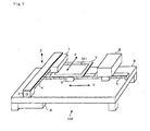
- FIG. 1 is a simplified diagonal view of an ink jet recording apparatus according to one embodiment of the present invention.
- an ink jet recording apparatus 100 comprises a set of ink jet head 1, an X-dimension drive shaft 4, a Y-dimension guide shaft 5, a controller 6, a mounting table 7, a cleaning mechanism unit 8, and a base platform 9.
- the set of ink jet head 1 comprises ink jet heads 1a that discharge ink that is a functional liquid supplied from an ink tank (not shown) from nozzles (discharge ports) thereof to pixels.
- the mounting table 7 is for mounting a color filter substrate 101 that is to be manufactured by this manufacturing apparatus, comprising a mechanism for securely holding that substrate in a standard position.
- the X-dimension drive shaft 4 is connected to an X-dimension drive motor 2.
- the X-dimension drive motor 2 is a stepping motor or the like which turns the X-dimension drive shaft 4 when supplied with an X-axis dimension drive signal from the controller 6.
- the X-dimension drive shaft 4 is turned, the set of ink jet head 1 moves in the X-axis direction.
- the Y-dimension guide shaft 5 is secured so that it does not move relative to the base platform 9.
- the mounting table 7 comprises a Y-dimension drive motor 3.
- the Y-dimension drive motor 3 is a stepping motor or the like which moves the mounting table 7 in the Y-axis direction when supplied with a Y-axis dimension drive signal from the controller 6.
- the set of ink jet head 1 can be freely moved to any location on the color filter substrate 101.
- the relative speed of the set of ink jet head 1, relative to the color filter substrate 101 can also be determined by the control of the drive mechanisms in each axial dimension.
- the controller 6 comprises a drive signal controller 31 (described further below) that supplies ink droplet discharge controlling signals to the set of ink jet head 1.
- the controller 6 also comprises a head position controller 32 (described further below) that supplies signals for controlling the positional relationship between the set of ink jet head 1 and the mounting table 7 to the X-dimension drive motor 2 and the Y-dimension drive motor 3.
- the cleaning mechanism unit 8 comprises a mechanism for cleaning the set of ink jet head 1.
- the cleaning mechanism unit 8 comprises a Y-dimension drive motor (not shown). By the drive of this Y-direction drive motor, the cleaning mechanism unit 8 moves along the Y-dimension guide shaft 5. The movement of the cleaning mechanism unit 8 is also controlled by the controller 6.
- Fig. 2 is an explanatory diagram of the structure of one of the individual ink jet heads 1a that configure a set of ink jet head 1.
- the ink jet head 1a is configured so as to comprise a nozzle plate 110, a pressure chamber base plate 120, and a vibration plate 130, as diagrammed in the figure. This head configures an on-demand type of piezo jet head.
- the pressure chamber base plate 120 comprises cavities (pressure chambers) 121, side walls (partitions) 122, a reservoir 123, and lead-in channels 124.
- the cavities 121 are formed by etching a substrate of silicon or the like and constitute space for storing ink or the like for the purpose of discharging it.
- the side walls 122 are formed so as make partitions between the cavities 121.
- the reservoir 123 forms a flow path for filling the cavities 121 with ink.
- the lead-in channels 124 are formed so that they can induct ink from the reservoir 123 into the cavities 121.
- the shapes of the cavities 121 and the like can be modified in various ways depending on the ink jet scheme. These may be made in the planar Kyser shape or in the cylindrical Zoltan shape, for example.
- the nozzle plate 110 is affixed to one surface of the pressure chamber base plate 120 so that the nozzles 111 are positioned so as to correspond with the cavities 121, respectively, provided in the pressure chamber base plate 120.
- the number of the nozzles 111 is not limited to the number diagrammed, however, and it is possible, for example, to have 32 nozzles in one line.
- the pressure chamber base plate 120 to which the nozzle plate 110 is affixed is accommodated in a frame 125 to configure the ink jet head la.
- the vibration plate 130 is affixed to the other surface of the pressure chamber base plate 120.
- the vibration plate 130 are provided piezoelectric elements (not shown) at portions thereof corresponding respectively to the positions of the cavities 121.
- a supply port (not shown) is provided in a portion of the vibration plate 130 corresponding to the position of the reservoir 123, making it possible to supply ink stored in an ink tank (not shown) to the interior of the pressure chamber base plate 120.
- the plurality of nozzles 111 is divided into a plurality of groups and the number of the group is fewer than the number of the nozzles 111. Described in greater detail, the configuration is such that the positions on the ink jet heads 1a where the plurality of nozzles 111 is arranged are divided into a plurality of areas, and the nozzles belonging to each area of that plurality of areas belong to a single group. Described in even greater detail, these groups comprise a group made up of a set of nozzles positioned close to the supply port, and a group made up of a set of nozzles positioned far from the supply port. Provision is made so that ink is discharged from the nozzles belonging to the same group by control signals having the same waveform, which control signals can be regulated group by group.
- Fig. 3 is a block diagram of the configuration of a control system for the ink jet recording apparatus 100 described above.
- the control system of ink jet recording apparatus 100 comprises a drive signal controller 31 and a head position controller 32 that are electronic computers such as personal computers.
- the drive signal controller 31 outputs a plurality of types of waveform for driving the ink jet heads 1a.
- the drive signal controller 31 also outputs bit map data indicating which color of ink, whether R, G, or B, to discharge to the pixels of the color filter.
- the drive signal controller 31 is connected to an analog amp 33 and a timing control circuit 34.
- the analog amp 33 is a circuit for amplifying the plurality of waveform types noted above.
- the timing control circuit 34 which has a built in clock pulse circuit, is a circuit for controlling the ink discharge timing according to the bit map data noted above.
- the analog amp 33 and the timing control circuit 34 are both connected to a relay circuit 35, and that relay circuit 35 is connected to a drive waveform selector circuit 36.
- the relay circuit 35 sends signals output from the analog amp 33 to the drive waveform selector circuit 36 according to the timing signals output from the timing control circuit 34.
- the drive waveform selector circuit 36 is a circuit for selecting, from the plurality of waveform types, waveforms for controlling the ink discharge from the ink jet heads 1a, and sending those to the ink jet heads 1a.
- the plurality of nozzles provided in the ink jet heads 1a are divided into a number of groups, that number being fewer than the number of nozzles, and one waveform is selected for each group. Which waveform of the plurality of waveform types to be selected for each group is set in the drive waveform selector circuit 36 on the basis of data on the quality of ink discharged from each nozzle in the ink jet heads 1a as measured beforehand.
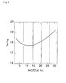
- Fig. 4 is a graph representing one example of ink discharge quantity distribution for the nozzles in the ink jet head described above. On the horizontal axis are plotted the nozzle numbers applied according to the arrangement of the plurality of nozzles provided in the ink jet head 1a, while on the vertical axis is plotted the discharge quantify (ng) per droplet of ink discharged from the nozzles when the same drive waveform is used for discharging ink from the nozzles.
- a single supply port is provided for supplying ink to the reservoir common to the nozzles. That supply port is positioned near the nozzles numbered 8 through 15. As indicated in this figure, the ink discharge quantity tends to be lower in the vicinity of the supply port, while that ink discharge quantity tends to be higher in the vicinities of the two ends which are far from the supply port.
- the head position controller 32 which is a circuit for controlling the positional relationship between the ink jet heads 1a and the mounting table 7 (together with the color filter substrate mounted thereon), works in conjunction with the drive signal controller 31 to effect control so that ink discharged from the ink jet heads 1a reaches prescribed locations on the color filter substrate.
- the head position controller 32 is connected to an X-Y control circuit 37 and sends information relating to head positions to that X-Y control circuit 37.
- the X-Y control circuit 37 is connected to the X-dimension drive motor 2 and the Y-dimension drive motor 3, and sends signals for controlling the position of the ink jet heads 1a in the X-axis dimension and the position of the mounting table 7 in the Y-axis dimension, based on signals from the head position controller 32, to the X-dimension drive motor 2 and the Y-dimension drive motor 3.
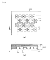
- Fig. 5 is an enlarged partial diagram of a color filter that is a functional liquid applied substrate manufactured by the manufacturing apparatus and manufacturing method relating to the embodiment described above.
- Fig. 5 (a is a plan, while Fig. 5(b) is a cross-sectional view at the B-3' line in Fig. 5(a) . Some of the hatching in portions of the cross-sectional view is omitted.
- the color filter 200 comprises pixels 13 lined up in a matrix form, with the boundaries between pixels demarcated by partitions 14. Into each individual pixel 13 is inducted ink of one or other of the colors red (R), green (G), and blue (B).
- R red
- G green
- B blue
- the arrangement of red, green, and blue is made the so-called delta arrangement, but this may be some other arrangement such as a strip arrangement or mosaic arrangement cr the like.
- the color filter 200 comprises a light transmitting substrate 12 and light blocking partitions 14.
- the portions where no partition 14 is formed (or where partition is removed) configure the pixels 13 noted above.
- the inks of several colors inducted to these pixels 13 configure coloring layers 20.
- An overcoat layer 21 and electrode layer 22 are formed on top of the partitions 14 and coloring layers 20.
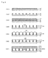
- Fig. 6 is a set of cross-sectional diagrams of the manufacturing processes for the color filter described above. Some of the hatching in portions of the cross-sectional views is omitted. Based on this figure, an example of the manufacturing method for the color filter is now described in specific terms.
- a transparent substrate 12 made of non-alkaline glass having a film thickness of 0.7 mm, longitudinal dimension of 38 cm, and lateral dimension of 30 cm, is washed with a washing liquid wherein 1 wt.% of hydrogen peroxide was added to hot concentrated sulfuric acid, rinsed with pure water, and air-dried to obtain a clean surface.
- a chromium film by a sputtering process, to an average film thickness of 0.2 ⁇ m, to yield a metal layer 16' (S1 in Fig. 6 ).
- This substrate is dried for 5 minutes at 80°C on a hot plate, after which a photoresist layer (not shown) is formed by spin coating onto the surface of the metal layer 16'.
- a mask film having a prescribed matrix pattern shape is securely affixed, and exposure is performed with UV radiation.
- an alkaline developing liquid containing potassium hydroxide in a ratio of 8 wt.% the portion of the photoresist not exposed is removed, and the resist layer is patterned.
- the exposed metal layer is removed by etching with an etching liquid the main component of which is hydrochloric acid.
- the light blocking layer 16 has a film thickness of about 0.2 ⁇ m and a width of about 22 ⁇ m.
- a negative type transparent acrylic photosensitive resin composition 17' again by spin coaling (S3 in Fig. 6 ).
- UV exposure is performed using a mask film whereon is drawn a prescribed matrix pattern shape.
- the unexposed portion of the resin is developed, again using an alkaline developing liquid, and, after rinsing with pure water, spin drying is performed.
- after-baking is performed for 30 minutes at 200°C, and the resin portions are thoroughly hardened.
- the bank layer 17 is formed, and both the light blocking layer 16 and the partitions 14 constituted by the bank layer 17 are formed (S4 in Fig. 6 ).
- the average film thickness of this bank layer 17 is 2.7 ⁇ m.
- the width of the bank layer 17 is about 14 ⁇ m.
- dry etching that is a plasma process under normal atmospheric pressure. More specifically, a high voltage is applied to a gas mixture wherein 20% oxygen has been added to helium, the plasma atmosphere is formed into an etching spot in normal atmospheric pressure, and the substrate is passed below that etching spot and etched.
- ink (functional liquid) is inducted by an ink jet method inside the pixels 13 formed by the demarcation of the partitions 14 (S5 in Fig. 6 ).
- minute ink droplets are selectively cast, 10 droplets per coloring layer formation area, using a precision head wherein a piezoelectric effect is employed.
- the drive frequency is set to 14.4 kHz, that is, the ink droplet discharge interval is set at 69.5 ⁇ sec.
- the distance between the head and the target is set at 0.3 mm.
- the waveform (inclusive of voltage) that drives the piezo elements of the head is crucial for the flight speed from the head to the coloring layer formation area (target) and for preventing the occurrence of flight curvature and what are called satellites (droplets that separate and go astray).
- the waveforms that drive the ink jet head are sent via the drive signal controller 31, analog amp 33, relay circuit 35, and drive waveform selector circuit 36 to the ink jet head.
- Fig. 7 is a waveform graph representing examples of signal waveforms of a plurality of types input to the drive waveform selection circuit 36 described earlier. Time ( ⁇ sec) is plotted on the horizontal axis, and the difference (V from the minimum value of the applied voltage is plotted on the vertical axis. Every one of the four types of waveform represented here is what is called a pull-push-pull type, wherewith, in the first stage where the voltage is caused to drop (pull), the ink is pulled into the meniscus, in the second stage where the voltage is caused to rise (push), the ink is discharged, and in the third stage where the voltage is again caused to drop pull), the meniscus vibration is caused to very rapidly diminish.
- a pull-push-pull type wherewith, in the first stage where the voltage is caused to drop (pull), the ink is pulled into the meniscus, in the second stage where the voltage is caused to rise (push), the ink is discharged, and in the third stage where the voltage is again caused to drop pull), the
- Vh the difference between the maximum value and minimum value of the applied voltage becomes 19 V, 19.5 V, 20 V, and 20.5 V, respectively.
- Vh the difference between the maximum value and minimum value of the applied voltage becomes 19 V, 19.5 V, 20 V, and 20.5 V, respectively.
- the drive waveform selector circuit 36 selects a waveform, from among the four types of waveform noted above, that control the ink discharge from the ink jet head 1a, and sends that waveform to the ink jet head 1a. More particularly, the 32 nozzles provided in the ink jet head 1a are divided into a total of five groups, comprising 7 nozzles, 7 nozzles, 6 nozzles, 6 nozzles, and 6 nozzles, respectively, and one waveform is selected for each group, respectively.
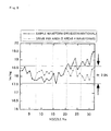
- Fig. 8 is a graph wherein are plotted pre-compensation and post-compensation data for the ink discharge quantity per droplet from the nozzles in the ink jet head 1a in this embodiment.
- On the horizontal axis are plotted nozzle numbers applied temporarily according to the arrangement of the nozzles, while on the vertical axis is plotted the discharge quantity (ng) per droplet from the nozzles.
- the pre-compensation data are indicated by the solid curved line, while the post-compensation data are indicated by the dotted curved line.
- the discharge quantity per ink droplet was calculated from the speed of the ink droplet discharged from the nozzle.
- the ink maximum discharge quantity from the nozzles was approximately 19.5 ng (nozzle No. 32), while the minimum was approximately 17.6 ng nozzle No. 16).
- the ink quantity variation was ⁇ 6.0%.
- the Vh of the signal for controlling the ink discharges from the nozzle group made up of No. 8 through No. 14 was made 20.5 V
- the Vh of the signal for controlling the ink discharges from the nozzle group made up of No. 21 through No. 26 was made 19.5 V
- the Vh of the signal for controlling the ink discharges from the nozzle group made up of No. 27 through No. 32 was made 19 V
- the maximum ink discharge quantity from the nozzles became approximately 18.6 ng (nozzle No. 24) and the minimum became approximately 17.6 ng (nozzle No. 16).
- the ink quantity variation was thus improved to ⁇ 2.9%.
- ink droplets are applied simultaneously in the three colors of red, green, and blue, and ink is applied in the prescribed color arrangement pattern.
- the ink used is made, for example, by dispersing an inorganic pigment in a polyurethane resin oligomer, then adding cyclohexanone and butyl acetate as low boiling point solvents and butylcarbitol acetate as a high boiling point solvent, and finally adding 0.01 wt.% of a nonionic surfactant as a dispersant to make the viscosity 6 to 8 centipoise.
- the applied ink is dried.
- the ink layer 19 is set by allowing it to stand for 3 hours in the natural atmosphere. Then heating is performed for 40 minutes at 80°C on a hot plate. Finally, heating is performed for 30 minutes at 200°C in an oven to perform the ink layer 19 hardening process to yield the coloring layers 20 (S6 in Fig. 6 ).
- the overcoat layer 21 having a smooth surface.
- the electrode layer 22 consisting of indium tin oxide (ITO) is formed in a prescribed pattern to make the color filter 200 (S7 in Fig. 6 ).
- Fig. 9 is a cross-sectional diagram of a color liquid crystal display device that is an electro-optical apparatus manufactured by the manufacturing method in one embodiment of the present invention. Some of the hatching in portions of the cross-sectional view is omitted.
- this color liquid crystal display device 300 because the color filter 200 manufactured by the method described above is used, the functional liquid discharge quantity is made more uniform between the pixels, and the film thickness of the functional liquid after drying and hardening becomes uniform between the pixels, whereupon images of good picture quality can be displayed therewith.
- This color liquid crystal display device 300 is configured by combining the color filter 200 with an opposing substrate 338, and sealing therebetween a liquid crystal composition 337.
- TFT thin film transistor
- pixel electrodes 332 are formed in a matrix form.
- the color filter 200 is deployed so that the red, green, and blue coloring layers 20 are arranged at positions corresponding to the pixel electrodes 332.
- orientation films 326 and 336 are formed on the surfaces that are opposed to the substrate 338 and the color filter 200, respectively. These orientation films 326 and 336 are subjected to a rubbing treatment, and the liquid crystal molecules can be arranged in a certain direction. To the outer surfaces of the substrate 338 and the color filter 200, furthermore, polarizing panels 329 and 339 are bonded, respectively. Also, a fluorescent lamp (not shown) and a scattering plate combination is commonly used for a backlight, and the display is effected by causing the liquid crystal composition 337 to function as an optical shutter that changes the transmissivity of the backlight.
- the electro-optical apparatus is not limited in the present invention to the color liquid crystal display device described above, but various apparatuses can be adopted, such as a thin picture tube, for example, or a small television receiver wherein a liquid crystal shutter or the like is used, or an electro-optical apparatus wherein any of various electro-optical means are used such as an EL display device, plasma display, CRT display, or field emission display (FED)
- a thin picture tube for example, or a small television receiver wherein a liquid crystal shutter or the like is used
- an electro-optical apparatus wherein any of various electro-optical means are used such as an EL display device, plasma display, CRT display, or field emission display (FED)
- Fig. 10 is a diagonal view of a notebook style personal computer manufactured by the manufacturing method of one embodiment of the present invention.
- this personal computer 500 because the color liquid crystal display device 30C described above is used as the display unit, the functional liquid discharge quantity is made more uniform between the pixels, and the film thickness of the functional liquid after drying and hardening becomes uniform between the pixels, whereupon images of good picture quality can be displayed therewith.
- the color liquid crystal display device 300 is accommodated in a case 510, and the configuration is such that the display area of the color liquid crystal display device 300 is exposed through an opening 511 formed in the case 510.
- the personal computer 500 also comprises a keyboard 530 as an input unit.
- This personal computer 500 is configured so as to contain, in addition to the color liquid crystal display device 300, a display signal generator comprising various circuits (not shown) such as a display information output source, display information processing circuit, and clock signal generation circuit, together with a power supply circuit for supplying electric power to those circuits.
- a display signal generator comprising various circuits (not shown) such as a display information output source, display information processing circuit, and clock signal generation circuit, together with a power supply circuit for supplying electric power to those circuits.
- display images are formed by the supply of display signals generated by the display signal generator based on information such as that input from the input unit 530, for example.
- the electronic equipment in which the electro-optical apparatus relating to this embodiment is incorporated is not limited to a personal computer, but may be any of various electronic equipment such as a portable telephone, electronic notebook, pager, POS terminal, IC card, mini disk player, liquid crystal projector, engineering work station (EWS), word processor, television receiver, viewfinder-type or monitor direct-view type video tape recorder, electronic desktop calculator, car navigation unit, device equipped with a touch panel, timepiece, or game equipment.
- a portable telephone electronic notebook, pager, POS terminal, IC card, mini disk player, liquid crystal projector, engineering work station (EWS), word processor, television receiver, viewfinder-type or monitor direct-view type video tape recorder, electronic desktop calculator, car navigation unit, device equipped with a touch panel, timepiece, or game equipment.
- EWS engineering work station
- the functional liquid applied substrate manufactured by the manufacturing apparatus and method of the present invention is not limited to the color filter described in the foregoing, moreover, but may also be an EL element substrate. In that case, a solution of an electroluminophor may be used as the functional liquid.
- the functional liquid applied substrate manufactured by the manufacturing apparatus and method of the present invention may also be a substrate whereon a conducting wiring pattern is formed.
- the functional liquid is an electrically conducting particle dispersion solution wherein a powdered form of an electrically conducting substance such as gold (Au), silver (Ag), copper (Cu), platinum (Pt), or palladium (Pd), a binder for bonding the powder, and a dispersant for dispersing the powder uniformly, and the like, are dissolved in a solvent.
- the electrically conducting particle dispersion solution is applied, using the ink jet head of the present invention, so that a prescribed conducting wiring pattern is formed on the substrate.
- the functional liquid is dried and hardened and the conducting wiring pattern is formed.
- the functional liquid applied substrate may also be a substrate whereon a semiconductor device is formed or a substrate whereon a memory configured by semiconductor devices is formed.
- a solution containing an inorganic semiconductor material, organic semiconductor material, electrically conductive polymer, or ferroelectric material or the like is used as the functional liquid.
- the functional liquid applied substrate may also be a substrate used as a sample in genetic analysis. In that case, a solution containing protein or deoxyribonucleic acid (DNA) is used as the functional liquid.
- a solution containing protein or deoxyribonucleic acid (DNA) is used as the functional liquid.
- the functional liquid applied substrate may also be a substrate that configures an electronic device such as the prime example of a substrate configuring a display electron gun. In that case, a solution containing carbon nanotubes is used as the functional liquid.
- the functional liquid applied substrate may also be a substrate that configures a catalyst in a fuel cell, or a catalyst used in non-electric field plating, or a field emission display (FED). In that case, a solution containing a precious metal and a precious metal salt or an oxide thereof is used as the functional liquid.
- FED field emission display
- an ink jet recording apparatus capable of making the discharge quantities of functional liquids more uniform by simple procedures and with a simple configuration, and a functional liquid applied substrate manufacturing method, are provided.
Landscapes
- Physics & Mathematics (AREA)
- General Physics & Mathematics (AREA)
- Optics & Photonics (AREA)
- Optical Filters (AREA)
- Electroluminescent Light Sources (AREA)
- Ink Jet (AREA)
- Particle Formation And Scattering Control In Inkjet Printers (AREA)
- Application Of Or Painting With Fluid Materials (AREA)
Claims (6)
- Tintenstrahlaufzeichnungsvorrichtung (100), umfassend:mehrere Düsen (111) zur Abgabe einer funktionellen Flüssigkeit (19);Hohlräume (121), die für jede der Düsen vorgesehen sind;piezoelektrische Elemente, die für jede der Düsen vorgesehen sind;ein Reservoir (123), das mit den Hohlräumen verbunden ist und den Düsen gemein ist;eine Zufuhröffnung zum Zuleiten der funktionellen Flüssigkeit zu dem Reservoir;mehrere Düsengruppen (111), von welchen jede mehrere der Düsen hat, wobei die Anzahl von Gruppen geringer ist als die Gesamtanzahl von Düsen (111), und jede Düsengruppe Düsen enthält, die nebeneinander liegen, undeine Antriebssteuerung, die konfiguriert ist zum Regulieren einer Abgabemenge und Fluggeschwindigkeit der funktionellen Flüssigkeit, die aus den Düsen für jede Düsengruppe ausgegeben wird, durch einen Spannungspegel, der an die piezoelektrischen Elemente, die den Düsen entsprechen, angelegt wird, wobei die Antriebssteuerung zur Ausgabe von Wellenformen geeignet ist, die den Spannungspegel bestimmen, wobei:die Positionen, an welchen die Düsen vorgesehen sind, in mehrere Flächen unterteilt sind und eine Wellenform für jede Fläche vorgesehen ist, von der angenommen wird, dass sie einen wechselseitig ähnlichen Abgabetrend aufweist,Düsen, die zu jeder Fläche gehören einer einzigen Gruppe zugeordnet sind,und die Antriebssteuerung dazu ausgebildet ist, die Wellenform für jede Düsengruppe auf der Basis der Abgabemenge und der Fluggeschwindigkeit der funktionellen Flüssigkeit zu wählen, wobei die Wellenform derart ist, dass der im Voraus gemessene Spannungspegel der Wellenform, die für Düsengruppen gewählt wird, die weiter von der Zufuhröffnung entfernt angeordnet sind, kleiner wird als der Spannungspegel der Wellenform, die für Düsengruppen gewählt wird, die näher der Zufuhröffnung angeordnet sind,wodurch für Düsengruppen, die weiter von der Zufuhröffnung entfernt angeordnet sind, die gewählte Wellenform dazu ausgebildet ist, die Abgabemenge zu verringern, und für Düsengruppen, die näher der Zufuhröffnung angeordnet sind, die gewählte Wellenform dazu ausgebildet ist, die Abgabemenge zu erhöhen.
- Tintenstrahlaufzeichnungsvorrichtung (100) nach Anspruch 1, wobei die mehreren Gruppen mindestens eine erste Gruppe umfassen, die Düsen (111) der mehreren Düsen (111) umfasst, die nahe der Zufuhröffnung positioniert sind, und eine zweite Gruppe, die Düsen (111) der mehreren Düsen (111) umfasst, die fern der Zufuhröffnung positioniert sind.
- Tintenstrahlaufzeichnungsvorrichtung (100) nach Anspruch 1, wobei sich der Spannungspegel, der an piezoelektrische Elemente angelegt wird, für jede der mehreren Gruppen unterscheidet, um eine Differenz der Tintenabgabemenge zwischen den Gruppen auszugleichen.
- Verfahren zur Herstellung eines Substrats, auf das funktionelle Flüssigkeit von einer Tintenstrahlaufzeichnungsvorrichtung (100) aufgetragen wird, wobei die Vorrichtung mehrere Düsen (111) zur Abgabe einer funktionellen Flüssigkeit (19); Hohlräume (121), die für jede der Düsen vorgesehen sind; piezoelektrische Elemente, die für jeden der Hohlräume (121) vorgesehen sind; ein Reservoir (123), das mit den Hohlräumen (121) verbunden ist und den Düsen (111) gemein ist; eine Zufuhröffnung zum Zuleiten der funktionellen Flüssigkeit (19) zu dem Reservoir (123); und mehrere Düsengruppen (111) umfasst, von welchen jede mehrere der Düsen hat, wobei die Anzahl von Gruppen geringer ist als die Gesamtanzahl von Düsen (111), und jede Düsengruppe Düsen enthält, die nebeneinander liegen,
wobei die Positionen, an welchen die Düsen vorgesehen sind, in mehrere Flächen unterteilt sind und eine Wellenform für jede Fläche vorgesehen ist, von der angenommen wird, dass sie einen wechselseitig ähnlichen Abgabetrend aufweist, wobei Düsen, die zu jeder Fläche gehören, einer einzigen Gruppe zugeordnet sind,
wobei das Verfahren umfasst:Regulieren mit einer Antriebssteuerung eines Spannungspegels für jede Düsengruppe, der an die piezoelektrischen Elemente, die den Düsen entsprechen, angelegt wird, zur Steuerung der Abgabemenge und Fluggeschwindigkeit der funktionellen Flüssigkeit aus den Düsen, wobei der Spannungspegel durch die Wellenform bestimmt wird, undAbgeben der funktionellen Flüssigkeit in Pixel, die auf einem Substrat gebildet werden,wobei die Regulierung das Wählen der Wellenform für jede Düsengruppe mit der Antriebssteuerung auf der Basis der Abgabemenge und der Fluggeschwindigkeit der funktionellen Flüssigkeit umfasst, wobei die Wellenform derart ist, dass der im Voraus gemessene Spannungspegel der Wellenform, die für Düsengruppen gewählt wird, die weiter von der Zufuhröffnung entfernt angeordnet sind, kleiner wird als der Spannungspegel der Wellenform, die für Düsengruppen gewählt wird, die näher der Zufuhröffnung angeordnet sind, wodurch für Düsengruppen, die weiter von der Zufuhröffnung entfernt angeordnet sind, die gewählte Wellenform dazu ausgebildet ist, die Abgabemenge zu verringern, und für Düsengruppen, die näher der Zufuhröffnung angeordnet sind, die gewählte Wellenform dazu ausgebildet ist, die Abgabemenge zu erhöhen. - Verfahren zur Herstellung eines Substrats, auf das funktionelle Flüssigkeit (19) aufgetragen wird, nach Anspruch 4, wobei die mehreren Gruppen mindestens eine erste Gruppe umfassen, die Düsen (111) der mehreren Düsen (111) umfasst, die nahe der Zufuhröffnung positioniert sind, und eine zweite Gruppe, die Düsen (111) der mehreren Düsen (111) umfasst, die fern der Zufuhröffnung positioniert sind.
- Verfahren zur Herstellung eines Substrats, auf das funktionelle Flüssigkeit aufgetragen wird, nach Anspruch 4, wobei sich der Spannungspegel, der an piezoelektrische Elemente angelegt wird, für jede der mehreren Gruppen unterscheidet, um eine Differenz der Tintenabgabemenge zwischen den Gruppen auszugleichen.
Applications Claiming Priority (5)
| Application Number | Priority Date | Filing Date | Title |
|---|---|---|---|
| JP2000316954 | 2000-10-17 | ||
| JP2000316954 | 2000-10-17 | ||
| JP2001318215A JP4182657B2 (ja) | 2000-10-17 | 2001-10-16 | インクジェット式記録装置 |
| JP2001318215 | 2001-10-16 | ||
| PCT/JP2001/009112 WO2002032582A1 (en) | 2000-10-17 | 2001-10-17 | Ink jet recorder and method of manufacturing functional liquid applied substrate |
Publications (3)
| Publication Number | Publication Date |
|---|---|
| EP1238708A1 EP1238708A1 (de) | 2002-09-11 |
| EP1238708A4 EP1238708A4 (de) | 2007-04-18 |
| EP1238708B1 true EP1238708B1 (de) | 2011-07-13 |
Family
ID=26602249
Family Applications (1)
| Application Number | Title | Priority Date | Filing Date |
|---|---|---|---|
| EP01976714A Expired - Lifetime EP1238708B1 (de) | 2000-10-17 | 2001-10-17 | Tintenstrahldrucker und herstellung eines substrats mit einer funktionellen flüssigkeit |
Country Status (7)
| Country | Link |
|---|---|
| US (1) | US6893103B2 (de) |
| EP (1) | EP1238708B1 (de) |
| JP (1) | JP4182657B2 (de) |
| KR (1) | KR100516754B1 (de) |
| CN (1) | CN1184074C (de) |
| TW (1) | TWI236971B (de) |
| WO (1) | WO2002032582A1 (de) |
Families Citing this family (89)
| Publication number | Priority date | Publication date | Assignee | Title |
|---|---|---|---|---|
| JP4720069B2 (ja) * | 2002-04-18 | 2011-07-13 | セイコーエプソン株式会社 | 電気光学装置及び電子機器 |
| US6890050B2 (en) | 2002-08-20 | 2005-05-10 | Palo Alto Research Center Incorporated | Method for the printing of homogeneous electronic material with a multi-ejector print head |
| JP4955919B2 (ja) * | 2002-09-30 | 2012-06-20 | セイコーエプソン株式会社 | 配線形成方法 |
| JP2004146796A (ja) | 2002-09-30 | 2004-05-20 | Seiko Epson Corp | 膜パターンの形成方法、薄膜製造装置、導電膜配線、電気光学装置、電子機器、並びに非接触型カード媒体 |
| CA2512011A1 (en) * | 2003-01-10 | 2004-07-29 | Qinetiq Nanomaterials Limited | Improvements in and relating to deposited structures |
| JP4033126B2 (ja) * | 2003-02-20 | 2008-01-16 | セイコーエプソン株式会社 | 燃料電池製造装置および燃料電池の製造方法 |
| JP2004290962A (ja) * | 2003-03-11 | 2004-10-21 | Seiko Epson Corp | 薄膜形成装置、電子光学装置及び電子機器 |
| JP3966292B2 (ja) * | 2003-03-27 | 2007-08-29 | セイコーエプソン株式会社 | パターンの形成方法及びパターン形成装置、デバイスの製造方法、導電膜配線、電気光学装置、並びに電子機器 |
| JP3760926B2 (ja) * | 2003-04-25 | 2006-03-29 | セイコーエプソン株式会社 | 液滴吐出装置、及び液滴吐出方法 |
| JP4675350B2 (ja) * | 2003-04-25 | 2011-04-20 | 株式会社半導体エネルギー研究所 | 液滴吐出装置 |
| JP4628109B2 (ja) * | 2003-04-25 | 2011-02-09 | 株式会社半導体エネルギー研究所 | 半導体装置の作製方法 |
| JP4689159B2 (ja) * | 2003-10-28 | 2011-05-25 | 株式会社半導体エネルギー研究所 | 液滴吐出システム |
| US7309563B2 (en) * | 2003-12-19 | 2007-12-18 | Palo Alto Research Center Incorporated | Patterning using wax printing and lift off |
| US8753702B2 (en) * | 2004-01-20 | 2014-06-17 | Fujifilm Dimatix, Inc. | Printing on edible substrates |
| US20080075859A1 (en) * | 2004-01-20 | 2008-03-27 | Baker Richard J | Printing, Depositing, or Coating On Flowable Substrates |
| JP3912384B2 (ja) * | 2004-02-10 | 2007-05-09 | セイコーエプソン株式会社 | 燃料電池の製造方法 |
| US7011529B2 (en) * | 2004-03-01 | 2006-03-14 | Anritsu Company | Hermetic glass bead assembly having high frequency compensation |
| JP4281584B2 (ja) * | 2004-03-04 | 2009-06-17 | セイコーエプソン株式会社 | 半導体装置の製造方法 |
| US20050255253A1 (en) * | 2004-05-13 | 2005-11-17 | White John M | Apparatus and methods for curing ink on a substrate using an electron beam |
| US20050253917A1 (en) * | 2004-05-13 | 2005-11-17 | Quanyuan Shang | Method for forming color filters in flat panel displays by inkjetting |
| JP2006078828A (ja) * | 2004-09-10 | 2006-03-23 | Toshiba Tec Corp | 液晶フィルタの製造装置 |
| US7556334B2 (en) * | 2004-11-04 | 2009-07-07 | Applied Materials, Inc. | Methods and apparatus for aligning print heads |
| US20070042113A1 (en) * | 2004-11-04 | 2007-02-22 | Applied Materials, Inc. | Methods and apparatus for inkjet printing color filters for displays using pattern data |
| US7413272B2 (en) * | 2004-11-04 | 2008-08-19 | Applied Materials, Inc. | Methods and apparatus for precision control of print head assemblies |
| US20060092218A1 (en) * | 2004-11-04 | 2006-05-04 | Applied Materials, Inc. | Methods and apparatus for inkjet printing |
| US20060109296A1 (en) * | 2004-11-04 | 2006-05-25 | Bassam Shamoun | Methods and apparatus for inkjet printing color filters for displays |
| US20060093751A1 (en) * | 2004-11-04 | 2006-05-04 | Applied Materials, Inc. | System and methods for inkjet printing for flat panel displays |
| US7050697B1 (en) | 2004-12-29 | 2006-05-23 | E. I. Du Pont De Nemours And Company | Pixel arrangement for organic electronic devices |
| US20060159843A1 (en) * | 2005-01-18 | 2006-07-20 | Applied Materials, Inc. | Method of substrate treatment for manufacturing of color filters by inkjet printing systems |
| US20060185587A1 (en) * | 2005-02-18 | 2006-08-24 | Applied Materials, Inc. | Methods and apparatus for reducing ink conglomerates during inkjet printing for flat panel display manufacturing |
| US7544723B2 (en) * | 2005-07-15 | 2009-06-09 | Applied Materials, Inc. | Blue printing ink for color filter applications |
| US20070015847A1 (en) * | 2005-07-15 | 2007-01-18 | Applied Materials, Inc. | Red printing ink for color filter applications |
| US7460267B2 (en) | 2005-07-15 | 2008-12-02 | Applied Materials, Inc. | Green printing ink for color filter applications |
| TWI318685B (en) * | 2005-07-28 | 2009-12-21 | Applied Materials Inc | Methods and apparatus for concurrent inkjet printing and defect inspection |
| US20070070132A1 (en) * | 2005-09-27 | 2007-03-29 | Fan-Cheung Sze | Inkjet delivery module |
| US20070070109A1 (en) * | 2005-09-29 | 2007-03-29 | White John M | Methods and systems for calibration of inkjet drop positioning |
| US20070076040A1 (en) * | 2005-09-29 | 2007-04-05 | Applied Materials, Inc. | Methods and apparatus for inkjet nozzle calibration |
| US20080018677A1 (en) * | 2005-09-29 | 2008-01-24 | White John M | Methods and apparatus for inkjet print head cleaning using an inflatable bladder |
| US20070068560A1 (en) * | 2005-09-29 | 2007-03-29 | Quanyuan Shang | Methods and apparatus for inkjet print head cleaning |
| US7611217B2 (en) * | 2005-09-29 | 2009-11-03 | Applied Materials, Inc. | Methods and systems for inkjet drop positioning |
| US8264137B2 (en) * | 2006-01-03 | 2012-09-11 | Samsung Electronics Co., Ltd. | Curing binder material for carbon nanotube electron emission cathodes |
| TWI328520B (en) * | 2006-02-07 | 2010-08-11 | Applied Materials Inc | Methods and apparatus for reducing irregularities in color filters |
| TWI328518B (en) * | 2006-03-24 | 2010-08-11 | Applied Materials Inc | Methods and apparatus for inkjet printing using multiple sets of print heads |
| US20070256709A1 (en) * | 2006-04-29 | 2007-11-08 | Quanyuan Shang | Methods and apparatus for operating an inkjet printing system |
| US20070252863A1 (en) * | 2006-04-29 | 2007-11-01 | Lizhong Sun | Methods and apparatus for maintaining inkjet print heads using parking structures with spray mechanisms |
| US20070263026A1 (en) * | 2006-04-29 | 2007-11-15 | Quanyuan Shang | Methods and apparatus for maintaining inkjet print heads using parking structures |
| US7992956B2 (en) * | 2006-06-07 | 2011-08-09 | Applied Materials, Inc. | Systems and methods for calibrating inkjet print head nozzles using light transmittance measured through deposited ink |
| US20080024548A1 (en) * | 2006-07-26 | 2008-01-31 | Applied Materials, Inc. | Methods and apparatus for purging a substrate during inkjet printing |
| US20080024532A1 (en) * | 2006-07-26 | 2008-01-31 | Si-Kyoung Kim | Methods and apparatus for inkjet printing system maintenance |
| WO2008013902A2 (en) * | 2006-07-28 | 2008-01-31 | Applied Materials, Inc. | Methods and apparatus for improved manufacturing of color filters |
| JP2008094044A (ja) * | 2006-10-16 | 2008-04-24 | Seiko Epson Corp | ヘッドユニットおよび液滴吐出装置、液状体の吐出方法、カラーフィルタの製造方法、有機el素子の製造方法、配線基板の製造方法 |
| US20080204501A1 (en) * | 2006-12-01 | 2008-08-28 | Shinichi Kurita | Inkjet print head pressure regulator |
| US7722145B2 (en) | 2006-12-28 | 2010-05-25 | Toshiba Tec Kabushiki Kaisha | Ink jet head driving apparatus and ink jet head driving method |
| JP2008171001A (ja) * | 2007-01-11 | 2008-07-24 | Applied Materials Inc | 共通軸周囲を回転可能な複数のプリントヘッドを用いて、処理量を増加するための方法、装置及びシステム |
| US7857413B2 (en) | 2007-03-01 | 2010-12-28 | Applied Materials, Inc. | Systems and methods for controlling and testing jetting stability in inkjet print heads |
| US20080259101A1 (en) * | 2007-03-23 | 2008-10-23 | Applied Materials, Inc. | Methods and apparatus for minimizing the number of print passes in flat panel display manufacturing |
| JP5076606B2 (ja) * | 2007-04-05 | 2012-11-21 | 凸版印刷株式会社 | 光学素子の製造方法、カラーフィルタの製造方法及び有機エレクトロルミネッセンス素子の製造方法 |
| JP5018191B2 (ja) * | 2007-04-05 | 2012-09-05 | 凸版印刷株式会社 | 光学素子の製造方法、カラーフィルタの製造方法及び有機エレクトロルミネッセンス素子の製造方法 |
| US7681986B2 (en) * | 2007-06-12 | 2010-03-23 | Applied Materials, Inc. | Methods and apparatus for depositing ink onto substrates |
| JP5266671B2 (ja) * | 2007-06-21 | 2013-08-21 | セイコーエプソン株式会社 | 液状体の吐出方法、有機el素子の製造方法、カラーフィルタの製造方法 |
| US7637587B2 (en) * | 2007-08-29 | 2009-12-29 | Applied Materials, Inc. | System and method for reliability testing and troubleshooting inkjet printers |
| JP5233231B2 (ja) * | 2007-10-03 | 2013-07-10 | セイコーエプソン株式会社 | 液晶表示装置、及び液晶表示装置の製造方法 |
| JP4609472B2 (ja) * | 2007-10-03 | 2011-01-12 | セイコーエプソン株式会社 | 液滴吐出装置およびその製造方法 |
| US20090109250A1 (en) * | 2007-10-26 | 2009-04-30 | Johnston Benjamin M | Method and apparatus for supporting a substrate |
| JP2009136720A (ja) * | 2007-12-04 | 2009-06-25 | Seiko Epson Corp | 液状体の吐出方法、液滴吐出装置およびカラーフィルタの製造方法 |
| KR20100110323A (ko) * | 2007-12-06 | 2010-10-12 | 어플라이드 머티어리얼스, 인코포레이티드 | 라인 스캔 카메라를 사용하여 기판 상의 픽셀 웰들에 증착된 잉크를 측정하기 위한 방법 및 장치 |
| WO2009076248A1 (en) * | 2007-12-06 | 2009-06-18 | Applied Materials, Inc. | Systems and methods for improving measurement of light transmittance through ink deposited on a substrate |
| JP4905380B2 (ja) | 2008-02-08 | 2012-03-28 | セイコーエプソン株式会社 | 駆動信号設定方法 |
| JP2009189954A (ja) * | 2008-02-14 | 2009-08-27 | Seiko Epson Corp | 駆動信号設定方法 |
| JP5169330B2 (ja) * | 2008-03-06 | 2013-03-27 | セイコーエプソン株式会社 | 薄膜形成方法 |
| US20090251504A1 (en) * | 2008-03-31 | 2009-10-08 | Applied Materials, Inc. | Systems and methods for wet in-situ calibration using measurement of light transmittance through ink deposited on a substrate |
| JP2010210853A (ja) * | 2009-03-10 | 2010-09-24 | Seiko Epson Corp | 液滴吐出装置、液滴吐出方法、及びカラーフィルターの製造方法 |
| JP2010217643A (ja) * | 2009-03-18 | 2010-09-30 | Seiko Epson Corp | 液滴吐出装置、液滴吐出方法、及びカラーフィルターの製造方法 |
| JP2010227762A (ja) * | 2009-03-26 | 2010-10-14 | Seiko Epson Corp | 液滴吐出装置、薄膜形成方法 |
| JP5423148B2 (ja) * | 2009-05-27 | 2014-02-19 | セイコーエプソン株式会社 | 液滴吐出方法及び液滴吐出装置 |
| EP2465678B1 (de) * | 2010-12-16 | 2013-08-07 | Agfa Graphics N.V. | System und Verfahren zur digitalen Erzeugung einer Druckvorlage mit einer Flüssigkeitströpfchenauftragungsvorrichtung |
| JP5387590B2 (ja) * | 2011-01-05 | 2014-01-15 | セイコーエプソン株式会社 | 駆動信号設定方法 |
| JP2012179842A (ja) * | 2011-03-02 | 2012-09-20 | Ricoh Co Ltd | 画像形成装置、画像補正方法、画像補正プログラムおよび画像形成システム |
| US9669627B2 (en) * | 2014-01-10 | 2017-06-06 | Fujifilm Dimatix, Inc. | Methods, systems, and apparatuses for improving drop velocity uniformity, drop mass uniformity, and drop formation |
| US9427992B2 (en) * | 2014-12-08 | 2016-08-30 | Xerox Corporation | System and method for lead edge release coating for improved media stripping in an aqueous inkjet printer |
| JP6546480B2 (ja) * | 2015-08-28 | 2019-07-17 | 株式会社ミマキエンジニアリング | 液体吐出装置及び液体吐出装置の調整方法 |
| US20180201014A1 (en) * | 2015-08-28 | 2018-07-19 | Mimaki Engineering Co., Ltd. | Liquid ejection apparatus and method for adjusting the same |
| JP2017064920A (ja) * | 2015-09-28 | 2017-04-06 | 株式会社ミマキエンジニアリング | 液体吐出装置及び液体吐出装置の調整方法 |
| JP2018061936A (ja) * | 2016-10-13 | 2018-04-19 | 東レエンジニアリング株式会社 | 塗布膜形成方法、及び、インクジェット塗布装置 |
| CN107128069B (zh) * | 2017-04-28 | 2019-07-02 | 京东方科技集团股份有限公司 | 调节喷墨打印装置的方法、喷墨打印方法、装置及其系统 |
| US10314934B2 (en) | 2017-06-26 | 2019-06-11 | The Procter & Gamble Company | System and method for dispensing material |
| WO2020110827A1 (ja) * | 2018-11-29 | 2020-06-04 | 京セラ株式会社 | 記録装置及び記録装置用プログラム |
| JP6919671B2 (ja) * | 2019-03-25 | 2021-08-18 | カシオ計算機株式会社 | 印刷装置及び印刷方法 |
| CN115298030B (zh) | 2020-03-18 | 2024-03-15 | 株式会社御牧工程 | 喷墨打印机和喷墨打印机的控制方法 |
Citations (2)
| Publication number | Priority date | Publication date | Assignee | Title |
|---|---|---|---|---|
| JPS59123670A (ja) * | 1982-12-28 | 1984-07-17 | Canon Inc | インクジエツトヘツド |
| US4558333A (en) * | 1981-07-09 | 1985-12-10 | Canon Kabushiki Kaisha | Liquid jet recording head |
Family Cites Families (20)
| Publication number | Priority date | Publication date | Assignee | Title |
|---|---|---|---|---|
| JPS5953182B2 (ja) | 1980-05-08 | 1984-12-24 | 株式会社リコー | マルチインクジエツトヘツド |
| DE3709206A1 (de) * | 1987-03-20 | 1988-09-29 | Standard Elektrik Lorenz Ag | Herstellverfahren fuer den leuchtschirm einer bildwiedergabevorrichtung |
| JP2746633B2 (ja) * | 1989-02-08 | 1998-05-06 | キヤノン株式会社 | 液体噴射記録装置 |
| JP2863241B2 (ja) * | 1990-02-02 | 1999-03-03 | キヤノン株式会社 | 記録ヘッドおよび記録ヘッド駆動方法 |
| JP3215147B2 (ja) * | 1991-04-05 | 2001-10-02 | 株式会社リコー | 液体噴射記録ヘッドの駆動方法 |
| US5874974A (en) * | 1992-04-02 | 1999-02-23 | Hewlett-Packard Company | Reliable high performance drop generator for an inkjet printhead |
| US6116714A (en) * | 1994-03-04 | 2000-09-12 | Canon Kabushiki Kaisha | Printing head, printing method and apparatus using same, and apparatus and method for correcting said printing head |
| US5831387A (en) * | 1994-05-20 | 1998-11-03 | Canon Kabushiki Kaisha | Image forming apparatus and a method for manufacturing the same |
| DE69725374T2 (de) * | 1996-04-19 | 2004-08-12 | Canon K.K. | Tintenstrahldruckverfahren und -gerät unter Verwendung einer Druckqualität verbessernden Flüssigkeit |
| JP3036436B2 (ja) | 1996-06-19 | 2000-04-24 | セイコーエプソン株式会社 | アクティブマトリックス型有機el表示体の製造方法 |
| JP3111905B2 (ja) | 1996-07-22 | 2000-11-27 | 東レ株式会社 | カラーフィルタの製造装置及び製造方法 |
| JP3313977B2 (ja) | 1996-08-02 | 2002-08-12 | キヤノン株式会社 | インクジェット記録方法およびインクジェット記録装置 |
| JPH10119283A (ja) | 1996-10-24 | 1998-05-12 | Canon Inc | 記録装置および記録ヘッド駆動方法および記憶媒体 |
| JPH10202851A (ja) | 1997-01-28 | 1998-08-04 | Fuji Xerox Co Ltd | インクジェット記録装置 |
| US6302517B1 (en) * | 1997-03-18 | 2001-10-16 | Seiko Epson Corporation | Printing apparatus and printing method using multiple nozzle groups |
| JPH1125851A (ja) * | 1997-05-09 | 1999-01-29 | Canon Inc | 電子源、その製造方法及び製造装置並びに画像形成装置及びその製造方法 |
| JPH1158704A (ja) | 1997-08-15 | 1999-03-02 | Mitsubishi Electric Corp | インクジェット記録装置 |
| US6126273A (en) * | 1998-04-30 | 2000-10-03 | Hewlett-Packard Co. | Inkjet printer printhead which eliminates unpredictable ink nucleation variations |
| US6428134B1 (en) * | 1998-06-12 | 2002-08-06 | Eastman Kodak Company | Printer and method adapted to reduce variability in ejected ink droplet volume |
| JP2001038892A (ja) | 1999-08-02 | 2001-02-13 | Seiko Epson Corp | 印刷装置、印刷方法、記録媒体およびノズルブロックの製造方法 |
-
2001
- 2001-10-16 US US09/977,339 patent/US6893103B2/en not_active Expired - Lifetime
- 2001-10-16 JP JP2001318215A patent/JP4182657B2/ja not_active Expired - Fee Related
- 2001-10-17 TW TW090125803A patent/TWI236971B/zh not_active IP Right Cessation
- 2001-10-17 CN CNB018051626A patent/CN1184074C/zh not_active Expired - Lifetime
- 2001-10-17 KR KR10-2002-7007765A patent/KR100516754B1/ko not_active Expired - Lifetime
- 2001-10-17 EP EP01976714A patent/EP1238708B1/de not_active Expired - Lifetime
- 2001-10-17 WO PCT/JP2001/009112 patent/WO2002032582A1/ja not_active Ceased
Patent Citations (2)
| Publication number | Priority date | Publication date | Assignee | Title |
|---|---|---|---|---|
| US4558333A (en) * | 1981-07-09 | 1985-12-10 | Canon Kabushiki Kaisha | Liquid jet recording head |
| JPS59123670A (ja) * | 1982-12-28 | 1984-07-17 | Canon Inc | インクジエツトヘツド |
Also Published As
| Publication number | Publication date |
|---|---|
| KR100516754B1 (ko) | 2005-09-22 |
| WO2002032582A1 (en) | 2002-04-25 |
| CN1184074C (zh) | 2005-01-12 |
| EP1238708A4 (de) | 2007-04-18 |
| CN1400927A (zh) | 2003-03-05 |
| JP4182657B2 (ja) | 2008-11-19 |
| JP2002196127A (ja) | 2002-07-10 |
| KR20020086864A (ko) | 2002-11-20 |
| EP1238708A1 (de) | 2002-09-11 |
| TWI236971B (en) | 2005-08-01 |
| US6893103B2 (en) | 2005-05-17 |
| US20020054197A1 (en) | 2002-05-09 |
Similar Documents
| Publication | Publication Date | Title |
|---|---|---|
| EP1238708B1 (de) | Tintenstrahldrucker und herstellung eines substrats mit einer funktionellen flüssigkeit | |
| US8780317B2 (en) | Film forming method, film forming device, liquid crystal arrangement method, liquid crystal arrangement device, liquid crystal device, liquid crystal device production method and electronic equipment | |
| US6364450B1 (en) | Color filter manufacturing method and apparatus, display device manufacturing method, method of manufacturing apparatus having display device, and display device panel manufacturing method and apparatus | |
| KR20040079854A (ko) | 성막 방법, 성막 장치, 컬러 필터 기판의 제조 방법 및제조 장치, 일렉트로루미네선스 장치용 기판의 제조 방법및 제조 장치, 표시 장치의 제조 방법, 표시 장치, 및전자 기기 | |
| KR100690539B1 (ko) | 액체 방울 토출 장치, 전기 광학 장치, 전기 광학 장치의제조 방법 및 전자 기기 | |
| JP3969034B2 (ja) | カラーフィルタの製造方法 | |
| CN1695945B (zh) | 液滴喷吐装置、电光学装置、电子设备以及液滴喷吐方法 | |
| JP3925525B2 (ja) | 液滴吐出装置、パネルの製造方法、画像表示装置および電子機器 | |
| JP3922517B2 (ja) | 機能性液体付与基板の製造方法、電気光学装置の製造方法、及び機能性液体付与基板の製造装置 | |
| US8715774B2 (en) | Liquid droplet ejection method | |
| US7691654B2 (en) | Method for manufacturing active matrix substrate, active matrix substrate, electro-optical device and electronic apparatus | |
| US7691562B2 (en) | Method for forming film pattern, and method for manufacturing device, electro-optical device, electronic apparatus and active matrix substrate | |
| JP4438039B2 (ja) | カラーフィルタの製造方法及び製造装置、液晶パネルの製造方法、表示装置の製造方法、表示装置用パネルの製造方法 | |
| EP1630869A2 (de) | Aktives Matrix-Substrat, Herstellungsverfahren für ein aktives Matrix-Substrat, Elektro-optisches Bauelement, und elektronische Vorrichtung | |
| US20070215713A1 (en) | Liquid material placing method, manufacturing method for electro-optical device, electro-optical device and electronic apparatus | |
| US7052099B2 (en) | Liquid drop ejecting device and liquid drop ejecting method, layer forming device and layer forming method, manufacturing for device, and electronic apparatus | |
| JP3978643B2 (ja) | カラーフィルタ、電気光学装置及び電子機器の製造方法 | |
| JP4427758B2 (ja) | カラーフィルタ及び電気光学装置の修復装置及び製造装置 | |
| JP2002219798A (ja) | インクジェット式記録装置および機能性液体付与基板の製造方法 | |
| JP2002122726A (ja) | カラーフィルタの製造方法、カラーフィルタ製造装置および記録装置 | |
| JP2007175701A (ja) | 液滴吐出装置、パネルの製造方法、画像表示装置および電子機器 |
Legal Events
| Date | Code | Title | Description |
|---|---|---|---|
| PUAI | Public reference made under article 153(3) epc to a published international application that has entered the european phase |
Free format text: ORIGINAL CODE: 0009012 |
|
| 17P | Request for examination filed |
Effective date: 20020612 |
|
| AK | Designated contracting states |
Kind code of ref document: A1 Designated state(s): AT BE CH CY DE DK ES FI FR GB GR IE IT LI LU MC NL PT SE TR |
|
| RBV | Designated contracting states (corrected) |
Designated state(s): AT BE CH DE FR GB LI |
|
| A4 | Supplementary search report drawn up and despatched |
Effective date: 20070319 |
|
| 17Q | First examination report despatched |
Effective date: 20080206 |
|
| GRAP | Despatch of communication of intention to grant a patent |
Free format text: ORIGINAL CODE: EPIDOSNIGR1 |
|
| RBV | Designated contracting states (corrected) |
Designated state(s): DE FR GB |
|
| GRAS | Grant fee paid |
Free format text: ORIGINAL CODE: EPIDOSNIGR3 |
|
| GRAA | (expected) grant |
Free format text: ORIGINAL CODE: 0009210 |
|
| AK | Designated contracting states |
Kind code of ref document: B1 Designated state(s): DE FR GB |
|
| REG | Reference to a national code |
Ref country code: GB Ref legal event code: FG4D |
|
| REG | Reference to a national code |
Ref country code: DE Ref legal event code: R096 Ref document number: 60144964 Country of ref document: DE Effective date: 20110901 |
|
| PLBE | No opposition filed within time limit |
Free format text: ORIGINAL CODE: 0009261 |
|
| STAA | Information on the status of an ep patent application or granted ep patent |
Free format text: STATUS: NO OPPOSITION FILED WITHIN TIME LIMIT |
|
| 26N | No opposition filed |
Effective date: 20120416 |
|
| REG | Reference to a national code |
Ref country code: DE Ref legal event code: R097 Ref document number: 60144964 Country of ref document: DE Effective date: 20120416 |
|
| PGFP | Annual fee paid to national office [announced via postgrant information from national office to epo] |
Ref country code: GB Payment date: 20141015 Year of fee payment: 14 Ref country code: FR Payment date: 20141008 Year of fee payment: 14 Ref country code: DE Payment date: 20141014 Year of fee payment: 14 |
|
| REG | Reference to a national code |
Ref country code: DE Ref legal event code: R119 Ref document number: 60144964 Country of ref document: DE |
|
| GBPC | Gb: european patent ceased through non-payment of renewal fee |
Effective date: 20151017 |
|
| PG25 | Lapsed in a contracting state [announced via postgrant information from national office to epo] |
Ref country code: DE Free format text: LAPSE BECAUSE OF NON-PAYMENT OF DUE FEES Effective date: 20160503 Ref country code: GB Free format text: LAPSE BECAUSE OF NON-PAYMENT OF DUE FEES Effective date: 20151017 |
|
| REG | Reference to a national code |
Ref country code: FR Ref legal event code: ST Effective date: 20160630 |
|
| PG25 | Lapsed in a contracting state [announced via postgrant information from national office to epo] |
Ref country code: FR Free format text: LAPSE BECAUSE OF NON-PAYMENT OF DUE FEES Effective date: 20151102 |