EP1239584A2 - Frequenznachlaufoszillator und Betriebsverfahren dafür - Google Patents
Frequenznachlaufoszillator und Betriebsverfahren dafür Download PDFInfo
- Publication number
- EP1239584A2 EP1239584A2 EP02251662A EP02251662A EP1239584A2 EP 1239584 A2 EP1239584 A2 EP 1239584A2 EP 02251662 A EP02251662 A EP 02251662A EP 02251662 A EP02251662 A EP 02251662A EP 1239584 A2 EP1239584 A2 EP 1239584A2
- Authority
- EP
- European Patent Office
- Prior art keywords
- saw resonator
- circuit
- capacitance
- inputs
- differential
- Prior art date
- Legal status (The legal status is an assumption and is not a legal conclusion. Google has not performed a legal analysis and makes no representation as to the accuracy of the status listed.)
- Granted
Links
Images

Classifications
-
- H—ELECTRICITY
- H03—ELECTRONIC CIRCUITRY
- H03B—GENERATION OF OSCILLATIONS, DIRECTLY OR BY FREQUENCY-CHANGING, BY CIRCUITS EMPLOYING ACTIVE ELEMENTS WHICH OPERATE IN A NON-SWITCHING MANNER; GENERATION OF NOISE BY SUCH CIRCUITS
- H03B5/00—Generation of oscillations using amplifier with regenerative feedback from output to input
- H03B5/30—Generation of oscillations using amplifier with regenerative feedback from output to input with frequency-determining element being electromechanical resonator
- H03B5/32—Generation of oscillations using amplifier with regenerative feedback from output to input with frequency-determining element being electromechanical resonator being a piezoelectric resonator
- H03B5/326—Generation of oscillations using amplifier with regenerative feedback from output to input with frequency-determining element being electromechanical resonator being a piezoelectric resonator the resonator being an acoustic wave device, e.g. SAW or BAW device
Definitions
- the present invention is directed, in general, to oscillator circuits and, more specifically, to employing low phase noise oscillators in noisy environments.
- Synchronous optical networks which provide very high data rate fiber optic links for communications, require low phase noise local oscillators for clock recovery.
- Phase noise and the resulting effect of signal edge jitter in the local oscillator output, limits the clock speed or pulse rate for clock recovery by contributing to the required pulse width or duration for accurate operation.
- the local oscillator employed in such applications should be frequency-tunable, allowing the local oscillator to be set or adjusted to a specific frequency to, for example, track frequency variations in the received clock signal.
- maintaining low phase noise and providing significant tune range for a local oscillator have proven to be conflicting objectives.
- the invention consists in a two port differential mode SAW resonator circuit comprising:
- the invention consists in an oscillator comprising:
- the invention consists in a method of tuning a SAW resonator circuit comprising the steps of:
- the invention secures the benefits of a low phase noise, wide tune range SAW oscillator in noisy environments by employing the tunable two port SAW resonator circuit within the oscillator in differential model connected to a differential amplifier circuit to create a differential oscillator.
- low phase noise/edge jitter is maintained, due to common mode rejection, even in hostile environments while providing sufficient tune range to track small frequency changes.
- the resulting differential mode SAW oscillator is thus well-suited for use, for instance, in clock recovery within SONET applications.
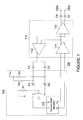
- Figure 1 depicts a circuit diagram for an exemplary differential mode oscillator including a two port tunable SAW resonator circuit according to one embodiment of the present invention.
- Differential mode oscillator 100 includes a two port SAW resonator 101 having a high input I H and a low input I L as well as a high output O H and a low output O L .
- FIG. 2A illustrates in greater detail the structure of a two port SAW resonator employed within the exemplary differential mode oscillator according to one embodiment of the present invention.
- Two port SAW resonator 101 constructed in accordance with the known art, includes: an input transducer 200 providing a first input terminal 201 for high input I H and a second input terminal 202 for low input I L ; an output transducer 210 providing a first input terminal 211 for high output O H and a second input terminal 212 for low output O L ; and reflectors 220.
- Figure 2B illustrates in greater detail an equivalent circuit for a two port SAW resonator 101 employed within the exemplary differential mode oscillator according to one embodiment of the present invention.
- the equivalent circuit of two port SAW resonator 101 includes a series resonator comprising a motional inductance L M , a motional capacitance C M and a motional resistance R M all connected in series.
- the series resonator is coupled to the inputs I H and I L and the outputs O H and O L by one-to-one, non-phase shifting transformers T 1 and T 2 .
- “Stray” capacitances C 01 and C 02 each formed by the internal parasitic and package capacitance (and any other unintentional capacitance) of the SAW resonator 101 as seen from one of the pairs of inputs I H and I L or outputs O H and O L , are each connected across the respective inputs I H and I L and outputs O H and O L in parallel with transformers T 1 and T 2 , respectively.
- SAW resonator 101 is made tunable by connecting at least one inductance L1 across at least one of the pairs of inputs I H and I L or outputs O H and O L (across inputs I H and I L in the exemplary embodiment).
- the inductance (a center-tap inductor with a DC return for varactors D1 and D2 in the example shown) is thus connected in parallel with the stray capacitances C 01 , and is sized to effectively tune out (i.e., resonate with) stray capacitance C 01 at the desired operational frequency.
- An additional inductance may optionally be connected across the outputs O H and O L , sized to effectively tune out stray capacitances C 02 .
- An inductance may be serially-connected within one or both of the differential signal lines to an input I H or I L , an output O H and O L , or both, and sized to effectively tune out stray capacitance(s) C 01 and/or C 02 .
- stray capacitance(s) C 01 and/or C 02 By tuning out stray capacitance(s) C 01 and/or C 02 , access is gained to the series resonator formed by motional inductance L M , motional capacitance C M and motional resistance R M , permitting direct tuning of the frequency at which the series resonator resonates.
- Variable capacitances D1 and D2, which are varactor diodes in the exemplary embodiment, are each connected to one of inputs I H and I L for this purpose. With stray capacitance C 01 tuned out, capacitances D1 and D2 alter the resonant frequency of the series resonator circuit formed by the series resonator within the equivalent circuit for the SAW resonator 101 and variable capacitances D1 and D2.
- tuning capacitances D1 and D2 decreases, the center frequency for the passband of the differential resonator circuit employing two port SAW resonator 101 increases.
- the desired tune range is thereby achieved with (because a high Q SAW device is employed) inherent low phase noise. If an inductance is employed coupled to the outputs O H and O L of SAW resonator 101, additional variable tuning capacitances (not shown) may be coupled to the outputs O H and O L .
- the motional capacitance C M should provide a high capacitive reactance, and therefore should be a very small capacitance on the order of femptoFarads (fF).
- fF femptoFarads
- a motional inductance L M on the order of milliHenrys (mH) is required.
- the stray capacitances C 01 and C 02 are (both) typically on the order of 1-2 picoFarads (pF).
- the motional capacitance C M employed for a single pole, two port SAW resonator 101 of the type disclosed should be as large as possible to allow tuning capacitances D1 and D2 to significantly impact the series resonator and provide acceptable tune range.
- the required motional capacitance is too small to be tuned.
- the same Q may be achieved using a larger motional capacitance C M .
- a suitable value for the motional capacitance C M is approximately 0.6 fF for a 622 MHz center frequency.
- a motional capacitance C M of approximately half that value would significantly reduce the tune range.
- a center tap inductor L1 having a total inductance of 56 nanoHenrys (nH) and tuning capacitances D1 and D2 having tuning ranges of approximately 2.0-0.4 pF may be employed.
- resistor R1 provides a direct current (DC) return through the center-tap of inductor L1 for biasing the varactors D1 and D2 while V TUNE , through series resistors R2 and R3, biases (and sets the capacitance values for) varactor diodes D1 and D2.
- DC direct current
- a tunable SAW resonator circuit 102 is thus formed by SAW resonator 101, inductor L1, varactor diodes D1 and D2, and resistors R1, R2 and R3.
- resistors R1, R2 and R3 each have a resistance of approximately 10 kiloOhms (k ⁇ ).
- Capacitors C1, C2, C6 and C7 which are direct current (DC) blocking capacitors, each have a capacitance of about 100 picoFarads (pF).
- additional inductances and variable tuning capacitances may be coupled to the outputs O H and O L of SAW resonator 101.
- an inductance may be connected in series (with one of tuning capacitances D1 or D2) to one of the inputs I H or I L (or in series with one of the outputs O H or O L ) and, if appropriately sized, approximately tune out the stray capacitance(s).
- a combination of series-connected and shunt inductances may also be employed to tune out the stray capacitance(s).
- the two port SAW resonator 101 in the present invention is employed in a differential mode.
- SAW resonator 101 is balanced, with no requirement that either input or output be either grounded or connected to a power supply voltage.
- a commercially-available differential amplifier circuit 110 designed for Pierce oscillators and including three differential amplifiers 111, 112 and 113 in the example shown, may be connected to the tunable SAW resonator circuit to create differential oscillator 100.
- Differential mode oscillator 100 provides common mode rejection, with the level of common mode rejection typically on the order of 30 decibels (dB) being determined by the degree of balance within the oscillator loop. This common mode rejection provides substantial noise immunity in hostile environments.
- Differential mode oscillator 100 preferably employs positive emitter coupled logic (PECL) signal levels.
- PECL positive emitter coupled logic
- both clock and inverse clock signals are usually desired.
- a differential oscillator 100 in accordance with the present invention, generating both signals is simplified.
- both output ports 102a and 102b may be employed separately as single-ended signals driving separate loads at power levels of +2 decibels with respect to a milliWatt (dBm).
- the differential mode oscillator 100 of the present invention does not have any critical tuning elements. Variances, such as manufacturing variances, in the sizes of inductance L1, the stray capacitances C 01 and C 02 , and tuning capacitances D1 and D2 may be tolerated without significant performance degradation.
- the tuning capacitances D1 and D2 within the exemplary embodiment need only have a capacitance of between 4 picoFarads (pF) and 2 picoFarads for low voltages, and less than approximately 0.4 pF for high voltages.
- the performance of oscillator 100 is almost entirely dependent on the SAW resonator characteristics, with no other critical requirements other than greater than unity gain, which is easily provided by a high gain amplifier.
- the differential mode SAW oscillator 100 of the present invention which is a voltage controlled SAW oscillator (VCSO) may be advantageously employed within the phase locked loop (PLL) of a clock recovery circuit, particularly for SONET applications.
- SAW oscillator 100 exhibits very low phase noise and edge jitter while providing sufficient tune range to track slight changes (error) in frequency during operation, allowing for manufacturing variances, and accommodating temperature variations.
Landscapes
- Oscillators With Electromechanical Resonators (AREA)
- Inductance-Capacitance Distribution Constants And Capacitance-Resistance Oscillators (AREA)
- Lock And Its Accessories (AREA)
- Burglar Alarm Systems (AREA)
- Apparatuses For Generation Of Mechanical Vibrations (AREA)
Applications Claiming Priority (2)
| Application Number | Priority Date | Filing Date | Title |
|---|---|---|---|
| US801452 | 2001-03-08 | ||
| US09/801,452 US6914493B2 (en) | 2001-03-08 | 2001-03-08 | Noise resistant low phase noise, frequency tracking oscillators and methods of operating the same |
Publications (3)
| Publication Number | Publication Date |
|---|---|
| EP1239584A2 true EP1239584A2 (de) | 2002-09-11 |
| EP1239584A3 EP1239584A3 (de) | 2003-08-27 |
| EP1239584B1 EP1239584B1 (de) | 2006-09-27 |
Family
ID=25181137
Family Applications (1)
| Application Number | Title | Priority Date | Filing Date |
|---|---|---|---|
| EP02251662A Expired - Lifetime EP1239584B1 (de) | 2001-03-08 | 2002-03-08 | Frequenznachlaufoszillator und Betriebsverfahren dafür |
Country Status (5)
| Country | Link |
|---|---|
| US (1) | US6914493B2 (de) |
| EP (1) | EP1239584B1 (de) |
| AT (1) | ATE341126T1 (de) |
| CA (1) | CA2375286A1 (de) |
| DE (1) | DE60214919T2 (de) |
Families Citing this family (9)
| Publication number | Priority date | Publication date | Assignee | Title |
|---|---|---|---|---|
| JP4138424B2 (ja) * | 2002-09-25 | 2008-08-27 | セイコーエプソン株式会社 | クロック変換器およびそのクロック変換器を備えた電子機器 |
| JP2006094242A (ja) * | 2004-09-24 | 2006-04-06 | Nippon Dempa Kogyo Co Ltd | 可変遅延型発振器 |
| US20070257728A1 (en) * | 2006-05-03 | 2007-11-08 | Sitime Corporation | Microelectromechanical multi-stage oscillator |
| US8446227B2 (en) * | 2009-02-04 | 2013-05-21 | Sand 9, Inc. | Methods and apparatus for tuning devices having mechanical resonators |
| US8456250B2 (en) * | 2009-02-04 | 2013-06-04 | Sand 9, Inc. | Methods and apparatus for tuning devices having resonators |
| US8395456B2 (en) | 2009-02-04 | 2013-03-12 | Sand 9, Inc. | Variable phase amplifier circuit and method of use |
| US8228127B2 (en) | 2009-12-23 | 2012-07-24 | Sand 9, Inc. | Oscillators having arbitrary frequencies and related systems and methods |
| EP3506500B1 (de) | 2017-12-07 | 2021-06-09 | Infineon Technologies AG | Bandsperrfilter basierend auf gekoppelten akustischen resonatoren |
| CN114337653A (zh) * | 2021-12-17 | 2022-04-12 | 青岛联众芯云科技有限公司 | 一种外置晶振补偿电容微调的通信系统及其控制方法 |
Family Cites Families (10)
| Publication number | Priority date | Publication date | Assignee | Title |
|---|---|---|---|---|
| GB2047491B (en) | 1979-04-02 | 1983-08-24 | Hewlett Packard Co | Oscillator mode suppression apparatus having bandpass effect |
| DE3305453A1 (de) * | 1983-02-17 | 1984-08-23 | Siemens AG, 1000 Berlin und 8000 München | Spannungsgesteuerter oszillator |
| US4581592A (en) | 1983-05-03 | 1986-04-08 | R F Monolithics, Inc. | Saw stabilized oscillator with controlled pull-range |
| EP0386498B1 (de) | 1989-02-17 | 1996-06-19 | Kabushiki Kaisha Toshiba | Oszillator |
| JPH0369203A (ja) | 1989-08-08 | 1991-03-25 | Alps Electric Co Ltd | 電圧制御発振器 |
| US5608360A (en) | 1995-11-03 | 1997-03-04 | Northrop Grumman Corporation | Oscillator formed of high frequency resonators and method of generating high frequency oscillator signal having reduced vibration sensitivity and phase noise and improved loop group delay |
| DE19634622B4 (de) | 1996-08-27 | 2005-05-12 | Epcos Ag | In seiner Resonanzfrequenz abstimmbarer Butler-Oszillator |
| JP3638434B2 (ja) * | 1998-05-29 | 2005-04-13 | 京セラ株式会社 | 弾性表面波装置 |
| US6239664B1 (en) | 1999-03-05 | 2001-05-29 | Rf Monolithics, Inc. | Low phase noise, wide tuning range oscillator utilizing a one port saw resonator and method of operation |
| US6426683B1 (en) * | 1999-11-09 | 2002-07-30 | Motorola, Inc. | Integrated filter with improved I/O matching and method of fabrication |
-
2001
- 2001-03-08 US US09/801,452 patent/US6914493B2/en not_active Expired - Fee Related
-
2002
- 2002-03-08 DE DE60214919T patent/DE60214919T2/de not_active Expired - Lifetime
- 2002-03-08 AT AT02251662T patent/ATE341126T1/de not_active IP Right Cessation
- 2002-03-08 EP EP02251662A patent/EP1239584B1/de not_active Expired - Lifetime
- 2002-03-08 CA CA002375286A patent/CA2375286A1/en not_active Abandoned
Also Published As
| Publication number | Publication date |
|---|---|
| US20020125964A1 (en) | 2002-09-12 |
| DE60214919T2 (de) | 2007-06-06 |
| US6914493B2 (en) | 2005-07-05 |
| CA2375286A1 (en) | 2002-09-08 |
| DE60214919D1 (de) | 2006-11-09 |
| EP1239584A3 (de) | 2003-08-27 |
| ATE341126T1 (de) | 2006-10-15 |
| EP1239584B1 (de) | 2006-09-27 |
Similar Documents
| Publication | Publication Date | Title |
|---|---|---|
| US6292065B1 (en) | Differential control topology for LC VCO | |
| US5561398A (en) | LC-tuned voltage controlled ring oscillator | |
| US7053722B2 (en) | Voltage controlled oscillator (VCO) with output buffer | |
| US7199674B2 (en) | Low phase noise, wide tune range saw oscillators and methods of operating the same | |
| EP0827641B1 (de) | Oszillator | |
| US6914493B2 (en) | Noise resistant low phase noise, frequency tracking oscillators and methods of operating the same | |
| US6472945B1 (en) | Operational amplifier oscillator | |
| EP1184968A2 (de) | Hochfrequenz- Kristalloszillator | |
| US20030034852A1 (en) | Oscillation circuit and electronics using the same | |
| US6661295B2 (en) | Controllable crystal oscillator | |
| JP2000236218A (ja) | 発振器および電圧制御型発振器 | |
| US20040263270A1 (en) | Oscillator circuit and oscillator | |
| KR20080061263A (ko) | 발진기 | |
| US7227421B2 (en) | Crystal oscillator circuit | |
| US7135936B2 (en) | Output buffer with inductive voltage divider | |
| EP0755112A1 (de) | Abstimmbarer spannungsgesteuerter Oszillator | |
| US5793261A (en) | Saw stabilized FSK oscillator circuit | |
| US6690244B2 (en) | Low phase-noise integrated voltage controlled oscillator | |
| US7564316B2 (en) | Variable-frequency oscillator incorporating thin-film bulk acoustic resonators | |
| US7692505B2 (en) | Crystal oscillator | |
| CN1035300C (zh) | 压控声表面波振荡器 | |
| US6297706B1 (en) | Single stage voltage controlled ring oscillator | |
| GB2408401A (en) | Improved coupling in a linearised varactor circuit | |
| US20050275480A1 (en) | Frequency selective oscillator, electronic instrument implementing the same, and method of adjusting frequency control characteristics | |
| EP1777808A1 (de) | Colpitts Hochfrequenzoszillatorschaltung |
Legal Events
| Date | Code | Title | Description |
|---|---|---|---|
| PUAI | Public reference made under article 153(3) epc to a published international application that has entered the european phase |
Free format text: ORIGINAL CODE: 0009012 |
|
| AK | Designated contracting states |
Kind code of ref document: A2 Designated state(s): AT BE CH CY DE DK ES FI FR GB GR IE IT LI LU MC NL PT SE TR |
|
| AX | Request for extension of the european patent |
Free format text: AL;LT;LV;MK;RO;SI |
|
| PUAL | Search report despatched |
Free format text: ORIGINAL CODE: 0009013 |
|
| AK | Designated contracting states |
Designated state(s): AT BE CH CY DE DK ES FI FR GB GR IE IT LI LU MC NL PT SE TR |
|
| AX | Request for extension of the european patent |
Extension state: AL LT LV MK RO SI |
|
| RIC1 | Information provided on ipc code assigned before grant |
Ipc: 7H 03B 5/12 B Ipc: 7H 03B 5/36 B Ipc: 7H 03B 5/32 A |
|
| 17P | Request for examination filed |
Effective date: 20040216 |
|
| 17Q | First examination report despatched |
Effective date: 20040322 |
|
| AKX | Designation fees paid |
Designated state(s): AT BE CH CY DE DK ES FI FR GB GR IE IT LI LU MC NL PT SE TR |
|
| GRAP | Despatch of communication of intention to grant a patent |
Free format text: ORIGINAL CODE: EPIDOSNIGR1 |
|
| GRAS | Grant fee paid |
Free format text: ORIGINAL CODE: EPIDOSNIGR3 |
|
| GRAA | (expected) grant |
Free format text: ORIGINAL CODE: 0009210 |
|
| AK | Designated contracting states |
Kind code of ref document: B1 Designated state(s): AT BE CH CY DE DK ES FI FR GB GR IE IT LI LU MC NL PT SE TR |
|
| PG25 | Lapsed in a contracting state [announced via postgrant information from national office to epo] |
Ref country code: IT Free format text: LAPSE BECAUSE OF FAILURE TO SUBMIT A TRANSLATION OF THE DESCRIPTION OR TO PAY THE FEE WITHIN THE PRESCRIBED TIME-LIMIT;WARNING: LAPSES OF ITALIAN PATENTS WITH EFFECTIVE DATE BEFORE 2007 MAY HAVE OCCURRED AT ANY TIME BEFORE 2007. THE CORRECT EFFECTIVE DATE MAY BE DIFFERENT FROM THE ONE RECORDED. Effective date: 20060927 Ref country code: AT Free format text: LAPSE BECAUSE OF FAILURE TO SUBMIT A TRANSLATION OF THE DESCRIPTION OR TO PAY THE FEE WITHIN THE PRESCRIBED TIME-LIMIT Effective date: 20060927 Ref country code: LI Free format text: LAPSE BECAUSE OF FAILURE TO SUBMIT A TRANSLATION OF THE DESCRIPTION OR TO PAY THE FEE WITHIN THE PRESCRIBED TIME-LIMIT Effective date: 20060927 Ref country code: FI Free format text: LAPSE BECAUSE OF FAILURE TO SUBMIT A TRANSLATION OF THE DESCRIPTION OR TO PAY THE FEE WITHIN THE PRESCRIBED TIME-LIMIT Effective date: 20060927 Ref country code: BE Free format text: LAPSE BECAUSE OF FAILURE TO SUBMIT A TRANSLATION OF THE DESCRIPTION OR TO PAY THE FEE WITHIN THE PRESCRIBED TIME-LIMIT Effective date: 20060927 Ref country code: CH Free format text: LAPSE BECAUSE OF FAILURE TO SUBMIT A TRANSLATION OF THE DESCRIPTION OR TO PAY THE FEE WITHIN THE PRESCRIBED TIME-LIMIT Effective date: 20060927 |
|
| REG | Reference to a national code |
Ref country code: GB Ref legal event code: FG4D |
|
| REG | Reference to a national code |
Ref country code: CH Ref legal event code: EP |
|
| REG | Reference to a national code |
Ref country code: IE Ref legal event code: FG4D |
|
| REF | Corresponds to: |
Ref document number: 60214919 Country of ref document: DE Date of ref document: 20061109 Kind code of ref document: P |
|
| PG25 | Lapsed in a contracting state [announced via postgrant information from national office to epo] |
Ref country code: DK Free format text: LAPSE BECAUSE OF FAILURE TO SUBMIT A TRANSLATION OF THE DESCRIPTION OR TO PAY THE FEE WITHIN THE PRESCRIBED TIME-LIMIT Effective date: 20061227 Ref country code: SE Free format text: LAPSE BECAUSE OF FAILURE TO SUBMIT A TRANSLATION OF THE DESCRIPTION OR TO PAY THE FEE WITHIN THE PRESCRIBED TIME-LIMIT Effective date: 20061227 |
|
| PG25 | Lapsed in a contracting state [announced via postgrant information from national office to epo] |
Ref country code: ES Free format text: LAPSE BECAUSE OF FAILURE TO SUBMIT A TRANSLATION OF THE DESCRIPTION OR TO PAY THE FEE WITHIN THE PRESCRIBED TIME-LIMIT Effective date: 20070107 |
|
| ET | Fr: translation filed | ||
| PG25 | Lapsed in a contracting state [announced via postgrant information from national office to epo] |
Ref country code: PT Free format text: LAPSE BECAUSE OF FAILURE TO SUBMIT A TRANSLATION OF THE DESCRIPTION OR TO PAY THE FEE WITHIN THE PRESCRIBED TIME-LIMIT Effective date: 20070313 |
|
| REG | Reference to a national code |
Ref country code: CH Ref legal event code: PL |
|
| PLBE | No opposition filed within time limit |
Free format text: ORIGINAL CODE: 0009261 |
|
| STAA | Information on the status of an ep patent application or granted ep patent |
Free format text: STATUS: NO OPPOSITION FILED WITHIN TIME LIMIT |
|
| 26N | No opposition filed |
Effective date: 20070628 |
|
| PG25 | Lapsed in a contracting state [announced via postgrant information from national office to epo] |
Ref country code: MC Free format text: LAPSE BECAUSE OF NON-PAYMENT OF DUE FEES Effective date: 20070331 Ref country code: IE Free format text: LAPSE BECAUSE OF NON-PAYMENT OF DUE FEES Effective date: 20070308 |
|
| PG25 | Lapsed in a contracting state [announced via postgrant information from national office to epo] |
Ref country code: GR Free format text: LAPSE BECAUSE OF FAILURE TO SUBMIT A TRANSLATION OF THE DESCRIPTION OR TO PAY THE FEE WITHIN THE PRESCRIBED TIME-LIMIT Effective date: 20061228 |
|
| PGFP | Annual fee paid to national office [announced via postgrant information from national office to epo] |
Ref country code: FR Payment date: 20080311 Year of fee payment: 7 |
|
| PGFP | Annual fee paid to national office [announced via postgrant information from national office to epo] |
Ref country code: IT Payment date: 20080329 Year of fee payment: 7 |
|
| PGFP | Annual fee paid to national office [announced via postgrant information from national office to epo] |
Ref country code: NL Payment date: 20080325 Year of fee payment: 7 |
|
| PG25 | Lapsed in a contracting state [announced via postgrant information from national office to epo] |
Ref country code: LU Free format text: LAPSE BECAUSE OF NON-PAYMENT OF DUE FEES Effective date: 20070308 Ref country code: CY Free format text: LAPSE BECAUSE OF FAILURE TO SUBMIT A TRANSLATION OF THE DESCRIPTION OR TO PAY THE FEE WITHIN THE PRESCRIBED TIME-LIMIT Effective date: 20060927 |
|
| PG25 | Lapsed in a contracting state [announced via postgrant information from national office to epo] |
Ref country code: TR Free format text: LAPSE BECAUSE OF FAILURE TO SUBMIT A TRANSLATION OF THE DESCRIPTION OR TO PAY THE FEE WITHIN THE PRESCRIBED TIME-LIMIT Effective date: 20060927 |
|
| NLV4 | Nl: lapsed or anulled due to non-payment of the annual fee |
Effective date: 20091001 |
|
| REG | Reference to a national code |
Ref country code: FR Ref legal event code: ST Effective date: 20091130 |
|
| PG25 | Lapsed in a contracting state [announced via postgrant information from national office to epo] |
Ref country code: NL Free format text: LAPSE BECAUSE OF NON-PAYMENT OF DUE FEES Effective date: 20091001 |
|
| PG25 | Lapsed in a contracting state [announced via postgrant information from national office to epo] |
Ref country code: FR Free format text: LAPSE BECAUSE OF NON-PAYMENT OF DUE FEES Effective date: 20091123 |
|
| PG25 | Lapsed in a contracting state [announced via postgrant information from national office to epo] |
Ref country code: IT Free format text: LAPSE BECAUSE OF NON-PAYMENT OF DUE FEES Effective date: 20090308 |
|
| PGFP | Annual fee paid to national office [announced via postgrant information from national office to epo] |
Ref country code: GB Payment date: 20160321 Year of fee payment: 15 |
|
| PGFP | Annual fee paid to national office [announced via postgrant information from national office to epo] |
Ref country code: DE Payment date: 20160330 Year of fee payment: 15 |
|
| REG | Reference to a national code |
Ref country code: DE Ref legal event code: R119 Ref document number: 60214919 Country of ref document: DE |
|
| GBPC | Gb: european patent ceased through non-payment of renewal fee |
Effective date: 20170308 |
|
| PG25 | Lapsed in a contracting state [announced via postgrant information from national office to epo] |
Ref country code: DE Free format text: LAPSE BECAUSE OF NON-PAYMENT OF DUE FEES Effective date: 20171003 |
|
| PG25 | Lapsed in a contracting state [announced via postgrant information from national office to epo] |
Ref country code: GB Free format text: LAPSE BECAUSE OF NON-PAYMENT OF DUE FEES Effective date: 20170308 |