EP1240366B1 - Reacteur de depot chimique en phase vapeur et chambre de traitement destinee a ce reacteur - Google Patents
Reacteur de depot chimique en phase vapeur et chambre de traitement destinee a ce reacteur Download PDFInfo
- Publication number
- EP1240366B1 EP1240366B1 EP00987325A EP00987325A EP1240366B1 EP 1240366 B1 EP1240366 B1 EP 1240366B1 EP 00987325 A EP00987325 A EP 00987325A EP 00987325 A EP00987325 A EP 00987325A EP 1240366 B1 EP1240366 B1 EP 1240366B1
- Authority
- EP
- European Patent Office
- Prior art keywords
- reactor
- flow
- gas
- base plate
- process chamber
- Prior art date
- Legal status (The legal status is an assumption and is not a legal conclusion. Google has not performed a legal analysis and makes no representation as to the accuracy of the status listed.)
- Expired - Lifetime
Links
Images


Classifications
-
- C—CHEMISTRY; METALLURGY
- C23—COATING METALLIC MATERIAL; COATING MATERIAL WITH METALLIC MATERIAL; CHEMICAL SURFACE TREATMENT; DIFFUSION TREATMENT OF METALLIC MATERIAL; COATING BY VACUUM EVAPORATION, BY SPUTTERING, BY ION IMPLANTATION OR BY CHEMICAL VAPOUR DEPOSITION, IN GENERAL; INHIBITING CORROSION OF METALLIC MATERIAL OR INCRUSTATION IN GENERAL
- C23C—COATING METALLIC MATERIAL; COATING MATERIAL WITH METALLIC MATERIAL; SURFACE TREATMENT OF METALLIC MATERIAL BY DIFFUSION INTO THE SURFACE, BY CHEMICAL CONVERSION OR SUBSTITUTION; COATING BY VACUUM EVAPORATION, BY SPUTTERING, BY ION IMPLANTATION OR BY CHEMICAL VAPOUR DEPOSITION, IN GENERAL
- C23C16/00—Chemical coating by decomposition of gaseous compounds, without leaving reaction products of surface material in the coating, i.e. chemical vapour deposition [CVD] processes
- C23C16/44—Chemical coating by decomposition of gaseous compounds, without leaving reaction products of surface material in the coating, i.e. chemical vapour deposition [CVD] processes characterised by the method of coating
- C23C16/455—Chemical coating by decomposition of gaseous compounds, without leaving reaction products of surface material in the coating, i.e. chemical vapour deposition [CVD] processes characterised by the method of coating characterised by the method used for introducing gases into reaction chamber or for modifying gas flows in reaction chamber
- C23C16/45502—Flow conditions in reaction chamber
- C23C16/45508—Radial flow
-
- C—CHEMISTRY; METALLURGY
- C23—COATING METALLIC MATERIAL; COATING MATERIAL WITH METALLIC MATERIAL; CHEMICAL SURFACE TREATMENT; DIFFUSION TREATMENT OF METALLIC MATERIAL; COATING BY VACUUM EVAPORATION, BY SPUTTERING, BY ION IMPLANTATION OR BY CHEMICAL VAPOUR DEPOSITION, IN GENERAL; INHIBITING CORROSION OF METALLIC MATERIAL OR INCRUSTATION IN GENERAL
- C23C—COATING METALLIC MATERIAL; COATING MATERIAL WITH METALLIC MATERIAL; SURFACE TREATMENT OF METALLIC MATERIAL BY DIFFUSION INTO THE SURFACE, BY CHEMICAL CONVERSION OR SUBSTITUTION; COATING BY VACUUM EVAPORATION, BY SPUTTERING, BY ION IMPLANTATION OR BY CHEMICAL VAPOUR DEPOSITION, IN GENERAL
- C23C16/00—Chemical coating by decomposition of gaseous compounds, without leaving reaction products of surface material in the coating, i.e. chemical vapour deposition [CVD] processes
- C23C16/44—Chemical coating by decomposition of gaseous compounds, without leaving reaction products of surface material in the coating, i.e. chemical vapour deposition [CVD] processes characterised by the method of coating
- C23C16/4412—Details relating to the exhausts, e.g. pumps, filters, scrubbers, particle traps
-
- C—CHEMISTRY; METALLURGY
- C23—COATING METALLIC MATERIAL; COATING MATERIAL WITH METALLIC MATERIAL; CHEMICAL SURFACE TREATMENT; DIFFUSION TREATMENT OF METALLIC MATERIAL; COATING BY VACUUM EVAPORATION, BY SPUTTERING, BY ION IMPLANTATION OR BY CHEMICAL VAPOUR DEPOSITION, IN GENERAL; INHIBITING CORROSION OF METALLIC MATERIAL OR INCRUSTATION IN GENERAL
- C23C—COATING METALLIC MATERIAL; COATING MATERIAL WITH METALLIC MATERIAL; SURFACE TREATMENT OF METALLIC MATERIAL BY DIFFUSION INTO THE SURFACE, BY CHEMICAL CONVERSION OR SUBSTITUTION; COATING BY VACUUM EVAPORATION, BY SPUTTERING, BY ION IMPLANTATION OR BY CHEMICAL VAPOUR DEPOSITION, IN GENERAL
- C23C16/00—Chemical coating by decomposition of gaseous compounds, without leaving reaction products of surface material in the coating, i.e. chemical vapour deposition [CVD] processes
- C23C16/44—Chemical coating by decomposition of gaseous compounds, without leaving reaction products of surface material in the coating, i.e. chemical vapour deposition [CVD] processes characterised by the method of coating
- C23C16/458—Chemical coating by decomposition of gaseous compounds, without leaving reaction products of surface material in the coating, i.e. chemical vapour deposition [CVD] processes characterised by the method of coating characterised by the method used for supporting substrates in the reaction chamber
- C23C16/4582—Rigid and flat substrates, e.g. plates or discs
- C23C16/4583—Rigid and flat substrates, e.g. plates or discs the substrate being supported substantially horizontally
- C23C16/4586—Elements in the interior of the support, e.g. electrodes, heating or cooling devices
-
- C—CHEMISTRY; METALLURGY
- C30—CRYSTAL GROWTH
- C30B—SINGLE-CRYSTAL GROWTH; UNIDIRECTIONAL SOLIDIFICATION OF EUTECTIC MATERIAL OR UNIDIRECTIONAL DEMIXING OF EUTECTOID MATERIAL; REFINING BY ZONE-MELTING OF MATERIAL; PRODUCTION OF A HOMOGENEOUS POLYCRYSTALLINE MATERIAL WITH DEFINED STRUCTURE; SINGLE CRYSTALS OR HOMOGENEOUS POLYCRYSTALLINE MATERIAL WITH DEFINED STRUCTURE; AFTER-TREATMENT OF SINGLE CRYSTALS OR A HOMOGENEOUS POLYCRYSTALLINE MATERIAL WITH DEFINED STRUCTURE; APPARATUS THEREFOR
- C30B25/00—Single-crystal growth by chemical reaction of reactive gases, e.g. chemical vapour-deposition growth
- C30B25/02—Epitaxial-layer growth
- C30B25/14—Feed and outlet means for the gases; Modifying the flow of the reactive gases
Definitions
- the invention relates to a chemical vapor deposition reactor comprising a process chamber containing wafers and flowing reactive gases to process said wafers and comprising means to prevent the reactive gases from exiting said process chamber but through a gas-collector.
- the invention finds an application in the industry of manufacturing chemical vapor deposition reactors for processing semiconductor devices, for example, gallium arsenide semiconductor devices.
- a chemical vapor deposition reactor is already known from the patent US-4,961,399.
- Said reactor has a planetary graphite substrate holder in a process chamber, which is the space where the gas flow is in contact with the wafers and is constituted by a cylindrical body, having a vertical axis and surrounding the planetary substrate holder as closely as possible.
- the cylindrical body is hermetically sealed at its lower and upper parts by bottom and top plates.
- a roughly flat cover covers this arrangement.
- An inlet for the reactive gas flow is located in the center of the cover, opposite to the planetary substrate holder.
- This inlet introduces the reactive gas flow into the process chamber via several concentric funnels whose ends flare downwardly.
- the cover is lifted to allow access to the interior of the process chamber.
- the substrate holder is surrounded by a hollow quartz ring provided with apertures around its circumference, which is an exhaust arrangement in which tubes end, via which the reactive gas flow can exit.
- An additional gas flow formed of hydrogen is fed in the space disposed between the cylindrical body and the quartz ring, in order to prevent the reactive gas flow to penetrate and contaminate said space.
- the above described reactor does not solve a certain number of problems.
- a problem is that the process chamber is not provided with sufficient means of isolation from peripheral spaces of the reactor. Said process chamber must be isolated in order to prevent the reactive gases flowing in said process chamber from exiting the process chamber and flowing towards spaces of said reactor other than said process chamber, contaminating said other spaces.
- the chemical reaction performed using reactive gas at high temperature leads to the creation of deposits, which are desirable on the wafers, but not desirable on all of the other spaces of the reactor. To avoid loss of function of those spaces, or change of epitaxial growth conditions, or deposit of foreign particles on the wafers during the action of loading / unloading said wafers by the accumulation of foreign deposits, those spaces have to be frequently cleaned.
- the actions to clean or replace said spaces create loss of useful time for the reactor.
- the contamination of spaces gets particularly important when the spaces exposed to the previously heated reactive gases are cool.
- the arsenic deposits on all surfaces below about 200 °C.
- the outer wall of the process chamber has to be cooled for many practical reasons, and its size and weight and the multiplicity of connections to it make that said chamber is not routinely easily opened for cleaning.
- This process chamber must also be isolated from the other reactor spaces in order to allow that the gas mixture composed of precursor gases to which the wafers are exposed can be changed very quickly as may be required by the process. Practically, after stopping the introduction of a precursor gas into the process chamber through the central inlet, the precursor gas concentration over the wafers should decrease by a factor 10000 in a few seconds. This is required, for example, when N-doping precursors are used during the growth of double doped structures such as High Electron Mobility Transistors denoted HEMT. This requirement can only be met if the reactive gases remain confined into the space fadng the wafers. All spaces other than that space should be exempt of reactive gases. Said process chamber must also be isolated because, in chemical vapor deposition process, the reactive gases used are usually dangerous and polluting and may not be allowed to flow outside the process chamber but through the plenum exhaust.
- said substrate holder is heated to temperatures in a range of 300 °C to 1500 °C to enable the chemical reaction. So, it is mainly made of a material both adapted to accommodate the wafers and to withstand such high temperatures, mainly graphic that presents the inconvenient to be porous.
- said substrate holder is rotating in order to ensure the wafers to be uniform between each others, and, also in order to influence the gas flow dynamics. The connection between a rotative axis and static parts is not easily tight and might form an exhaust for the reactive gas flow. So, the process chamber is not easily hermetically sealed from the space beneath the substrate holder.
- a chemical vapor deposition reactor comprising a process chamber containing wafers and flowing reactive gases to process said wafers and comprising means for isolating said process chamber as claimed in Claim 1.
- the gas pressure inside the process chamber is not allowed to be substantially different from the atmospheric pressure value.
- the inert gas for forming a counter-flow is to be introduced in a way that does not disturb the process pressure value, i. e. the amount of inert gas for forming an effective counter-flow is not allowed to be too important whichever the peripheral length of the movable elements of the process chamber.
- Too great an amount of inert gas to prevent the flowing reactive process gases from exiting the reactor chamber might mix with, and dilute said gases, and might disturb the process performed inside the process chamber. So, due to the fact that the inert gas is not allowed to disturb the process, it must be introduced in an other area than the process gases because the odds that it mixes with the process gases are too important.
- Advantages of the invention are that these means are easier to manufacture and to use, and are more efficient that the means already known of the state of the art: the layers deposited on the wafers are more uniform; the spaces external to the deposit chambers are kept clean; the volume of counter-flow gas is kept as small as possible; the pressure inside the deposit chamber is easily maintained at a required level.
- the invention relates to a chemical vapor deposition chamber referred to as process chamber for accommodating for example several semiconductor wafers.
- the invention also relates to a chemical vapor deposition reactor having such a process chamber.
- the process chamber has isolation elements to prevent the reactive gases present in the process chamber to exit said process chamber and flow towards the other parts of said reactor.
- the process chamber also has movable elements for opening/closing operation.
- the isolation elements and the movable element are provided with specific high temperature seal means structures and with a specific counter-flow to achieve the isolation of the process chamber.
- high temperatures it is to be understood temperatures of the order of, or higher than, 300°C, for example in the range of 300 to 1500°C.
- the invention finds an application for example in the industry of manufacturing gallium arsenide semiconductor devices.
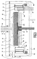
- a reactor is roughly cylindrical having a vertical axis.
- the reactor is provided with a circular base plate 30, for example having a diameter of about 25 cm, which in turn supports a rotating substrate holder 4A, 4B, on which one or several semiconductor wafers 5 are placed.
- the substrate holder has a rotating axis 4C passing through an opening 32 of the base plate 30.
- Heating means 7, as known of those skilled in the art, are disposed beneath the base plate 30 to heat the substrate holder 4A.
- the substrate holder is made of an appropriate material to accommodate the wafers and to be resilient to the process temperature, preferably graphite. However the graphite has the inconvenient to be porous and might let the reactive gases exit from the process chamber.
- This base plate 30 is arranged within the reactor in such a way that the reactive gases are In contact with the wafers.
- the reactor comprises a cylindrical body 19C having a vertical axis, which surrounds the base plate 30.
- On the lower and upper parts of said cylindrical body 19C are placed a bottom plate 19A and a roughly flat cover 28, respectively.
- the cylindrical body 19C being in a cold area of the reactor, the tightness with the bottom plate 19A and the cover 28 is ensured by toric joints 21, the bottom plate being preferably an horizontal part 19A of the cylindrical body 19C.
- the cover 28 can be lifted to place the base plate 30.
- This gas-collector is crown-shaped and comprises an annular top part 15, and an annular low part 14, said top and low parts being connected by lateral flanges 17 and 18. Screws 13 regularly spaced hold the top part 15 and the low part 14 together with the flanges 17, 18.
- the processing chamber 101 is limited by the flange 18 of the crown-shaped gas-collector 16.
- the flange 18 surrounding the substrate holder 4A has apertures 12 regularly spaced to let the reactive gases exhaust from the process chamber 101 and be lead by the gas-collector 16 towards a gas plenum 29.
- the gas plenum 29 is a tube having a wall 29A, which is provided with external longitudinal ridges 29B.
- the gas plenum 29 slides Into an aperture 40 of the annular low part 14, leaving small apertures 29C between the internal part 41 of the aperture 40 and the wall 29A of the gas plenum tube.
- the metal for forming the gas-collector may be favorably molybdenum.
- This gas-collector made of molybdenum presents the advantages of not involving the risk of exerting excessive forces onto the cover plate and base plate, of supporting the temperature prevailing in the chamber at the level of the semiconductor wafers and of being resistant to the processing gases use.
- two tubes 29 arranged diametrically opposite to each other merge into the interior of the gas-collector 16 to discharge the gases to the exterior.
- the inlet tube 1b has an extension 20 that Is bound to the cover 28, so that the inlet tubes 1A, 1B are lifted together with the cover 28 during an opening/closing operation of the reactor and so that this extension 20 forms the actual cover, hereafter referred to as cover plate 20, for the space immediately above the wafers 5 and substrate holder 4A.
- cover plate 20 Preferably the base plate 30, cover plate 20 and inlets 1A, 1B are made of quartz that is a non-porous material resilient to the high temperatures of the process.
- isolation means prevent the reactive gases from flowing into spaces of the reactor other than the space immediately above the substrate holder and the wafers, referred to as first space 101, and hereafter denoted process chamber, in fact containing the substrate holder 4A with the wafers 5, the inlets 1A, 1B and the gas-collector 16.
- Said isolation means comprise in detail:
- Said outer ring 10 surrounds the gas-collector 16 and the substrate holder 4A with the wafers 5 and touches both the base plate 30 and the cover plate 20, in such a manner that the first space denoted process chamber 101 containing the process gases is isolated from a second space 102 and third space 103 disposed externally to the outer ring 10 and plates 30 and 20, within the peripheral wall 19C, 19A.
- the outer ring 10 is disposed on the edge of the base plate 30, and has upper and lower flat surfaces for touching the base plate 30 and the extension cover 20. This outer ring 10 is preferably made of inox.
- the gas-collector 16 is not necessarily part of the isolating elements. It stands on the edge of the base plate 30 in such a way that it does not touch the cover plate 20 for allowing dilations due the high temperature gases collected.
- Said annular non-porous element 4B has an outer diameter that is greater than the diameter of the opening 32 for the rotating axis 4C, in order to prevent the reactive gases to exit through said opening 32.
- the base plate 30 is heated by the heating elements 7 at a temperature above 300°C, so the element 4B is constituted of a refractory metal apt to admit such temperatures.
- the non-porous element 4B of the substrate holder 4A is associated to the base plate 30 to particularly isolate the process chamber 101 from the third space 103.
- a counter-flow ⁇ 2 of non-reactive gas is applied in areas far from the reactive gases i. e. is introduced in the peripheral third space 103 through an inlet 39. This counter-flow propagates in the space 102 and is applied to the process chamber in a direction opposite to the reactive gases by way of specific structures referred to as high temperature seal means.
- seal means are small grooves or roughened zones of surfaces of the interfaces of the isolation elements above-described.
- the seal means structures are applied to the flat contact surfaces of the outer ring 10 at the interfaces with the cover plate 20 and the base plate 30.
- the seal means structures according to the invention avoid the processing gases from exiting through said interfaces, and force said process gases through the outlets 12 and then through the exhaust plenum 29. These seal means do not allow those process gases to enter the spaces 102, 103.
- the seal means are described in detail hereafter.
- the process gases located in the first space 101 of the process chamber, form a gas flow ⁇ 1 that has a pressure P1 slightly above the external atmospheric pressure, which results in that said gas flow ⁇ 1 propagates in a first direction D1 and tends to exit from the process chamber 101 through said Interface I.
- the seal means structures according to the invention first comprises the application of the counter-flow denoted ⁇ 2 of inert gas that is introduced for instance by an inlet 39 into the second and third spaces 102, 103, around the outer ring 10, that has a pressure P2 slightly above the pressure P1, which results In that said gas flow ⁇ 2 propagates in a second opposite direction D2 and tends to enter the process chamber 101 through said interface I.
- the counter-flow ⁇ 2 of inert gas propagates through the interface I as a laminar flow with a parabolic speed profile.
- the laminar flow speed V2 of the counter-flow is maximum in the middle of the small height of the interface I, while said laminar flow speed V2 is near zero along the so-called contact surfaces of the interface I.
- the first flow ⁇ 1 that has an inferior pressure P1 is not allowed to exit the process chamber 101 through the interface I.
- the propagation of laminar gas flow is related to the height H of the interface I, and to the difference of pressure between the flow and the counter-flow and also that the speed V2 of the counter-flow ⁇ 2 is function of this height H.
- a necessary speed V2 to make the counter-flow efficient implies that the difference of pressure between the flow and counter-flow or the squared height H 2 of the interface is not too small. It has been previously explained that the pressure difference P2 - P1 is not allowed to be great in order not to disturb the deposition process. Now, it is also important that the height H of the interface be not too large in order not to use a great amount of inert gas, which may also disturb the deposition process. As a matter of fact, it must be taken into account that the peripheral length of the processing chamber is important for accommodating several wafers, so that the amount of inert gas entering through the interface I may happen to be too great.
- the seal means structures according to the invention comprises the formation, on at least one of the two opposite contact surfaces, of a set of substantially radial grooves, performed along a length at least equal to the radial dimension of the upper and lower surfaces of the outer ring, for the counter-flow ⁇ 2 to enter the chamber 101 through said grooves.
- the depth and the width of a groove, and the width between two adjacent grooves are to be determined with respect to the length of the outer ring 10 in order to reach the aims of the invention.
- simulations are performed by calculation means of a standard kind according to known standard methods of calculation, which permit of determining those proper values.
- roughened zones of the contact surfaces of the considered interface may be used.
- the functions of the outer ring is to both to constitute an isolating element and to comprise seal means structures allowing the entry of an appropriate counter-flow ⁇ 2.
- the counter-flow ⁇ 2 propagates substantially through the grooves in the direction D2, i. e. from the space 102 towards the inside of the processing chamber 101.
- the gas flow ⁇ 1 which cannot propagate through the grooves due to the value of the counter-flow ⁇ 2, may however propagate between the grooves, through the still existing interface I. If the width between grooves is too important, said flow ⁇ 1 may propagate through the whole length of the interface I from the chamber 101 until it reaches the space 102, which is inconvenient. It why all the parameters of propagation of the counter-flow ⁇ 2 and flow ⁇ 1 are carefully calculated as above-described.
- the gas flow ⁇ 1 is no more allowed to exit the chamber 101 through the interface I, because, due to said appropriate ratio, the gas flow ⁇ 1 cannot get throughout the whole length of the grooves.
- the counter-flow ⁇ 2 is introduced by the inlet 39. It is shown that both the flow ⁇ 1 and the counter-flow ⁇ 2 are collected by the outlets 12, and then by the exhaust plenum 29. So, the gas flow ⁇ 1 exits through the gas-collector 16, being not allowed to get through the interface I and the counter-flow ⁇ 2 does not disturb the process.
- the pressure difference P2 - P1 is about 10 -5 to 10 3 mbars, which is considered a small difference of pressure;
- the height H of the interface I between closing surfaces is about 0 to 1 mm, preferably 0.05 to 0.1mm, which is considered small;
- the width and the depth of the grooves are about 1mm and 0.3mm respectively; and the ratio giving the width between grooves is 5 times the width of the groove.
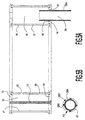
- the reactor comprises the base plate in two parts : a first ring-shaped base plate part 30A, which is disposed beneath the substrate holder 4A, and a second ring-shaped base plate part 30B, which supports the first ring-shaped base plate part 30A, the gas-collector 16 and the outer ring 10.
- the second ring-shaped base plate part 30B is movable downwards with respect to the first ring-shaped base plate part 30A in order to create free access to the wafers above the outer ring and the gas-collector.
- An aperture 40 is made in the peripheral wall 19C associated to a movable window 19B, referred to as gate valve, in order to create an access to the wafers when the second ring-shaped base plate part 30B is in the lowest position shown FIG.3.
- the arm of a robot may be used to manipulate the wafers.
- the contact surfaces of the first ring-shaped base plate part 30A and the second ring-shaped base plate part 30B are provided with seal means structures as above-described.
- the reactor comprises holes 55 and 58 provided in the outer ring 10 and the gas-collector 16 respectively, in order to introduce a tube 57.
- a light beam is guided for permitting of examining the wafers and for example of determining their rotation speed.
- the light beam may be introduced through the tube 57 for instance through a window 52, transparent to said light beam, and covering an aperture 53.
- the transparent window 52 may be bonded to the peripheral wall 19C at a part 51.
- a transparent solid material, referred to as tube window 56 is inserted so as to permit the operation of the counter-flow ⁇ 2 created by the difference of pressures between the second space and the first space each side of said tube window.
Landscapes
- Chemical & Material Sciences (AREA)
- General Chemical & Material Sciences (AREA)
- Chemical Kinetics & Catalysis (AREA)
- Engineering & Computer Science (AREA)
- Materials Engineering (AREA)
- Metallurgy (AREA)
- Organic Chemistry (AREA)
- Mechanical Engineering (AREA)
- Crystallography & Structural Chemistry (AREA)
- Chemical Vapour Deposition (AREA)
Claims (14)
- Un réacteur de dépôt chimique en phase vapeur, ayant une chambre de traitement (101) logeant un support de substrat (4a) pour des tranches (5), une première entrée (1A, 1B) amenant un premier courant gazeux (1) de gaz réactifs pour traiter les tranches, et un collecteur de gaz en forme de couronne entourant le support de substrat, ledit collecteur de gaz formant un espace annulaire creux et comprenant des ouvertures (12) pour laisser les gaz réactifs s'échapper de la chambre de traitement, dans lequel ledit réacteur comprend en outre :une plaque de base (30) et une plaque de couverture (20) disposées respectivement au-dessous et au-dessus du support de substrat,un anneau extérieur (10) entourant le collecteur de gaz (16) et touchant à la fois la plaque de base (30) et la plaque de couverture (20),dans lequel la chambre de traitement définit un premier espace (101), lequel premier espace est délimité par les plaques de base et de couverture, l'anneau extérieur et par une entrée (39) pour un deuxième courant (2) de gaz non réactifs,caractérisé en ce que le premier espace (101) est entouré par des deuxième et troisième espaces limités par une paroi périphérique pratiquement cylindrique (19C), une paroi horizontale inférieure (19A) et un couvercle (28), dans lequel une paroi comprend l'entrée pour le deuxième courant (2) et en ce que ledit deuxième courant agit en tant que contre-courant (2) pour empêcher le premier courant de gaz réactifs (1) de sortir de la chambre de traitement ailleurs que par le collecteur de gaz.
- Un réacteur selon la revendication 1, dans lequel l'anneau extérieur (10) a des surfaces supérieure et inférieure planes pour toucher les plaques de couverture et de base respectivement, et dans lequel lesdites surfaces supérieure et inférieure sont pourvues de rainures ou de zones rugueuses pour permettre au deuxième courant de gaz d'agir comme contre-courant (2) à travers les interfaces entre l'anneau extérieur et les plaques de couverture et de base.
- Un réacteur selon l'une des revendications 1 et 2, dans lequel le support de substrat (4A) est supporté par un axe tournant (4C), qui pénètre dans la chambre de traitement (101) à travers un trou (32) dans la plaque de base (30).
- Un réacteur selon la revendication 3, dans lequel ledit axe est relié au support de substrat (4A) par une partie annulaire (4B) qui est plus grande que le trou (32) dans la plaque de base (30) pour l'axe tournant (4C), dans lequel ladite partie annulaire (4B) reliant le support de substrat à l'axe tournant est faite d'un matériau moins poreux que le support de substrat.
- Un réacteur selon la revendication 4, dans lequel les températures de traitement sont dans la plage allant environ de 300 à 1500 °C et dans lequel ladite partie annulaire (4B) reliant le support de substrat (4A) à l'axe tournant (4C) est faite d'un matériau qui est en outre apte à résister à des températures aussi élevées.
- Un réacteur selon l'une des revendications 1 à 5, dans lequel la plaque de base comprend une première partie de plaque de base interne en forme d'anneau (30A) disposée sous le support de substrat et une deuxième partie de plaque de base périphérique en forme d'anneau (30B) supportant la première partie de plaque de base en forme d'anneau (30A), le collecteur de gaz (16) et l'anneau extérieur (10), la deuxième partie de plaque de base en forme d'anneau (30B) pouvant être déplacée par rapport à la première partie de plaque de base en forme d'anneau (30A) vers le bas pour créer un accès libre aux tranches pour une opération de manipulation des tranches.
- Un réacteur selon la revendication 6, dans lequel la paroi périphérique (19A) comprend une vanne à obturateur pour créer un accès aux tranches.
- Un réacteur selon l'une des revendications 6 et 7, dans lequel les surfaces de contact des première et deuxième parties de plaque de base en forme d'anneau (30A, 30B) sont pourvues de rainures ou de zones rugueuses pour permettre au deuxième courant de gaz (2) d'agir comme contre-courant à travers l'interface entre lesdites surfaces de contact.
- Un réacteur selon l'une des revendications 1 à 8, dans lequel un tube (57) est inséré à travers des trous (55, 58) pratiqués respectivement à travers l'anneau extérieur (10) et le collecteur de gaz (16) afin d'introduire un faisceau lumineux pour examiner les tranches sur le support de substrat.
- Un réacteur selon la revendication 9, dans lequel une pièce de matériau solide (56), appelée fenêtre tubulaire, transparente au faisceau lumineux, est introduite à l'intérieur du tube (57) de telle façon que les surfaces de contact du tube et de la fenêtre tubulaire permettent au deuxième courant (2) d'agir comme contre-courant pour empêcher le premier courant de gaz réactif de sortir de la chambre de traitement (101).
- Un réacteur selon la revendication 10, dans lequel la paroi périphérique cylindrique (19C) présente une fenêtre (52) transparente au faisceau lumineux pour introduire ledit faisceau lumineux à travers le tube (57).
- Un réacteur selon l'une des revendications 1 à 11, dans lequel des moyens de chauffage (7) sont prévus sous la plaque de base pour chauffer le support de substrat.
- Un réacteur selon l'une des revendications 1 à 12, dans lequel le collecteur de gaz est constitué d'une partie supérieure annulaire (15), d'une partie inférieure annulaire (14), lesdites parties supérieure et inférieure étant reliées par des brides latérales (17, 18) et maintenues ensemble par des vis (13), et dans lequel la bride faisant face au support de substrat comprend des sorties (12) pour le premier courant de gaz réactif.
- Un réacteur selon l'une des revendications 1 à 13, dans lequel une conduite de gaz (29) pour collecter les gaz provenant du collecteur de gaz comprend un tube (29) glissant dans des trous (40) du collecteur de gaz et de la plaque de base, et ledit tube (29) a des parois (29A) pourvues de saillies (29B) créant un espace entre le tube (29) et les bords (41) des trous (40) pour permettre au deuxième courant de gaz (2) d'agir comme contre-courant.
Priority Applications (1)
| Application Number | Priority Date | Filing Date | Title |
|---|---|---|---|
| EP00987325A EP1240366B1 (fr) | 1999-12-22 | 2000-11-30 | Reacteur de depot chimique en phase vapeur et chambre de traitement destinee a ce reacteur |
Applications Claiming Priority (4)
| Application Number | Priority Date | Filing Date | Title |
|---|---|---|---|
| EP99403255 | 1999-12-22 | ||
| EP99403255 | 1999-12-22 | ||
| EP00987325A EP1240366B1 (fr) | 1999-12-22 | 2000-11-30 | Reacteur de depot chimique en phase vapeur et chambre de traitement destinee a ce reacteur |
| PCT/EP2000/011992 WO2001046498A2 (fr) | 1999-12-22 | 2000-11-30 | Reacteur de depot chimique en phase vapeur et chambre de traitement destinee a ce reacteur |
Publications (2)
| Publication Number | Publication Date |
|---|---|
| EP1240366A2 EP1240366A2 (fr) | 2002-09-18 |
| EP1240366B1 true EP1240366B1 (fr) | 2003-07-09 |
Family
ID=8242229
Family Applications (1)
| Application Number | Title | Priority Date | Filing Date |
|---|---|---|---|
| EP00987325A Expired - Lifetime EP1240366B1 (fr) | 1999-12-22 | 2000-11-30 | Reacteur de depot chimique en phase vapeur et chambre de traitement destinee a ce reacteur |
Country Status (8)
| Country | Link |
|---|---|
| US (1) | US6899764B2 (fr) |
| EP (1) | EP1240366B1 (fr) |
| JP (1) | JP4809562B2 (fr) |
| KR (1) | KR100722592B1 (fr) |
| AT (1) | ATE244780T1 (fr) |
| DE (1) | DE60003850T2 (fr) |
| TW (1) | TW552626B (fr) |
| WO (1) | WO2001046498A2 (fr) |
Cited By (2)
| Publication number | Priority date | Publication date | Assignee | Title |
|---|---|---|---|---|
| WO2011023512A1 (fr) | 2009-08-25 | 2011-03-03 | Aixtron Ag | Procédé cvd et réacteur cvd |
| GB2571248B (en) * | 2018-01-11 | 2022-07-13 | Paragraf Ltd | A method of making Graphene layer structures |
Families Citing this family (71)
| Publication number | Priority date | Publication date | Assignee | Title |
|---|---|---|---|---|
| DE10043599A1 (de) * | 2000-09-01 | 2002-03-14 | Aixtron Ag | Vorrichtung zum Abscheiden insbesondere kristalliner Schichten auf einem oder mehreren insbesondere ebenfalls kristalliner Substraten |
| DE10043601A1 (de) * | 2000-09-01 | 2002-03-14 | Aixtron Ag | Vorrichtung und Verfahren zum Abscheiden insbesondere kristalliner Schichten auf insbesondere kristallinen Substraten |
| DE10133914A1 (de) * | 2001-07-12 | 2003-01-23 | Aixtron Ag | Prozesskammer mit abschnittsweise unterschiedlich drehangetriebenem Boden und Schichtabscheideverfahren in einer derartigen Prozesskammer |
| DE10153463A1 (de) * | 2001-10-30 | 2003-05-15 | Aixtron Ag | Verfahren und Vorrichtung zum Abscheiden insbesondere kristalliner Schichten auf insbesondere kristallinen Substraten |
| US6911092B2 (en) * | 2002-01-17 | 2005-06-28 | Sundew Technologies, Llc | ALD apparatus and method |
| DE10320597A1 (de) | 2003-04-30 | 2004-12-02 | Aixtron Ag | Verfahren und Vorrichtung zum Abscheiden von Halbleiterschichten mit zwei Prozessgasen, von denen das eine vorkonditioniert ist |
| US20050150452A1 (en) * | 2004-01-14 | 2005-07-14 | Soovo Sen | Process kit design for deposition chamber |
| US7431772B2 (en) * | 2004-03-09 | 2008-10-07 | Applied Materials, Inc. | Gas distributor having directed gas flow and cleaning method |
| JP4542860B2 (ja) * | 2004-10-04 | 2010-09-15 | 大陽日酸株式会社 | 気相成長装置 |
| JP4542859B2 (ja) * | 2004-10-04 | 2010-09-15 | 大陽日酸株式会社 | 気相成長装置 |
| JP2006128485A (ja) * | 2004-10-29 | 2006-05-18 | Asm Japan Kk | 半導体処理装置 |
| DE102005056320A1 (de) * | 2005-11-25 | 2007-06-06 | Aixtron Ag | CVD-Reaktor mit einem Gaseinlassorgan |
| JP5347294B2 (ja) * | 2007-09-12 | 2013-11-20 | 東京エレクトロン株式会社 | 成膜装置、成膜方法及び記憶媒体 |
| US8673080B2 (en) | 2007-10-16 | 2014-03-18 | Novellus Systems, Inc. | Temperature controlled showerhead |
| US8021487B2 (en) * | 2007-12-12 | 2011-09-20 | Veeco Instruments Inc. | Wafer carrier with hub |
| US20110114022A1 (en) * | 2007-12-12 | 2011-05-19 | Veeco Instruments Inc. | Wafer carrier with hub |
| KR100960958B1 (ko) * | 2007-12-24 | 2010-06-03 | 주식회사 케이씨텍 | 박막 증착 장치 및 증착 방법 |
| FR2930561B1 (fr) * | 2008-04-28 | 2011-01-14 | Altatech Semiconductor | Dispositif et procede de traitement chimique en phase vapeur. |
| JP5453768B2 (ja) * | 2008-11-05 | 2014-03-26 | 豊田合成株式会社 | 化合物半導体製造装置、化合物半導体の製造方法、および化合物半導体製造用治具 |
| JP2010171388A (ja) * | 2008-12-25 | 2010-08-05 | Hitachi Kokusai Electric Inc | 基板処理装置及び半導体装置の製造方法及び基板処理用反応管 |
| US8163089B2 (en) * | 2009-12-16 | 2012-04-24 | Primestar Solar, Inc. | Vapor deposition apparatus and process for continuous deposition of a thin film layer on a substrate |
| KR20110093476A (ko) * | 2010-02-12 | 2011-08-18 | 삼성엘이디 주식회사 | 기상 증착 시스템, 발광소자 제조방법 및 발광소자 |
| JP5410348B2 (ja) * | 2010-03-26 | 2014-02-05 | 株式会社豊田中央研究所 | 表面処理装置 |
| KR101313262B1 (ko) | 2010-07-12 | 2013-09-30 | 삼성전자주식회사 | 화학 기상 증착 장치 및 이를 이용한 반도체 에피 박막의 제조 방법 |
| US9920418B1 (en) | 2010-09-27 | 2018-03-20 | James Stabile | Physical vapor deposition apparatus having a tapered chamber |
| CN102465280B (zh) * | 2010-11-04 | 2013-11-27 | 上海蓝光科技有限公司 | 双面生长型mocvd反应器 |
| SG192967A1 (en) | 2011-03-04 | 2013-09-30 | Novellus Systems Inc | Hybrid ceramic showerhead |
| WO2012127305A1 (fr) * | 2011-03-21 | 2012-09-27 | Centrotherm Photovoltaics Ag | Alimentation en gaz pour four de traitement |
| DE102011002145B4 (de) * | 2011-04-18 | 2023-02-09 | Aixtron Se | Vorrichtung und Verfahren zum großflächigen Abscheiden von Halbleiterschichten mit gasgetrennter HCI-Einspeisung |
| DE102011002146B4 (de) * | 2011-04-18 | 2023-03-09 | Aixtron Se | Vorrichtung und Verfahren zum Abscheiden von Halbleiterschichten mit HCI-Zugabe zur Unterdrückung parasitären Wachstums |
| US9512520B2 (en) * | 2011-04-25 | 2016-12-06 | Applied Materials, Inc. | Semiconductor substrate processing system |
| JP5630393B2 (ja) * | 2011-07-21 | 2014-11-26 | 東京エレクトロン株式会社 | 成膜装置及び基板処理装置 |
| US20140174350A1 (en) * | 2011-08-09 | 2014-06-26 | Samsung Electronics Co., Ltd. | Vapor deposition apparatus |
| US20130171350A1 (en) * | 2011-12-29 | 2013-07-04 | Intermolecular Inc. | High Throughput Processing Using Metal Organic Chemical Vapor Deposition |
| KR101390963B1 (ko) | 2011-12-29 | 2014-05-07 | 엘아이지에이디피 주식회사 | 화학기상 증착용 공정 시스템 |
| JP2013191768A (ja) * | 2012-03-14 | 2013-09-26 | Sharp Corp | 成膜装置、成膜方法及び半導体素子 |
| US9816184B2 (en) * | 2012-03-20 | 2017-11-14 | Veeco Instruments Inc. | Keyed wafer carrier |
| USD712852S1 (en) | 2012-03-20 | 2014-09-09 | Veeco Instruments Inc. | Spindle key |
| US9388494B2 (en) | 2012-06-25 | 2016-07-12 | Novellus Systems, Inc. | Suppression of parasitic deposition in a substrate processing system by suppressing precursor flow and plasma outside of substrate region |
| KR101395206B1 (ko) * | 2012-11-30 | 2014-05-15 | 세메스 주식회사 | 기판 처리 장치 및 방법 |
| US9029809B2 (en) | 2012-11-30 | 2015-05-12 | Ultratech, Inc. | Movable microchamber system with gas curtain |
| US9399228B2 (en) * | 2013-02-06 | 2016-07-26 | Novellus Systems, Inc. | Method and apparatus for purging and plasma suppression in a process chamber |
| WO2014191622A1 (fr) * | 2013-05-29 | 2014-12-04 | Beneq Oy | Barrière, agencement support et procédé de prévention de croissance d'une matière |
| KR101518398B1 (ko) * | 2013-12-06 | 2015-05-08 | 참엔지니어링(주) | 기판 처리 장치 |
| KR101538461B1 (ko) * | 2013-12-06 | 2015-07-22 | 참엔지니어링(주) | 기판 처리 장치 |
| TWI654333B (zh) * | 2013-12-18 | 2019-03-21 | 美商蘭姆研究公司 | 具有均勻性折流板之半導體基板處理設備 |
| US10741365B2 (en) * | 2014-05-05 | 2020-08-11 | Lam Research Corporation | Low volume showerhead with porous baffle |
| US9793096B2 (en) * | 2014-09-12 | 2017-10-17 | Lam Research Corporation | Systems and methods for suppressing parasitic plasma and reducing within-wafer non-uniformity |
| KR102372893B1 (ko) * | 2014-12-04 | 2022-03-10 | 삼성전자주식회사 | 발광 소자 제조용 화학 기상 증착 장치 |
| US10378107B2 (en) | 2015-05-22 | 2019-08-13 | Lam Research Corporation | Low volume showerhead with faceplate holes for improved flow uniformity |
| US10023959B2 (en) | 2015-05-26 | 2018-07-17 | Lam Research Corporation | Anti-transient showerhead |
| KR20160144307A (ko) * | 2015-06-08 | 2016-12-16 | 울트라테크 인크. | 국소 처리가스 분위기를 이용한 마이크로챔버 레이저 처리 시스템 및 방법 |
| US9758868B1 (en) | 2016-03-10 | 2017-09-12 | Lam Research Corporation | Plasma suppression behind a showerhead through the use of increased pressure |
| US10403474B2 (en) | 2016-07-11 | 2019-09-03 | Lam Research Corporation | Collar, conical showerheads and/or top plates for reducing recirculation in a substrate processing system |
| KR102369676B1 (ko) | 2017-04-10 | 2022-03-04 | 삼성디스플레이 주식회사 | 표시 장치의 제조장치 및 표시 장치의 제조방법 |
| CN109321894B (zh) * | 2017-07-31 | 2021-06-08 | 北京北方华创微电子装备有限公司 | 一种增强清洗效果的沉积系统及方法 |
| FR3084136B1 (fr) | 2018-07-20 | 2021-01-29 | Valeo Vision | Dispositif lumineux matriciel avec estimation de temps de vol |
| FR3086724B1 (fr) | 2018-09-28 | 2022-10-14 | Valeo Vision | Source lumineuse matricielle pilotee en tension a circuit diagnostic pour un vehicule automobile |
| FR3086725B1 (fr) | 2018-09-28 | 2022-10-14 | Valeo Vision | Source lumineuse matricielle a circuit diagnostic pour un vehicule automobile |
| FR3086723B1 (fr) | 2018-09-28 | 2022-08-12 | Valeo Vision | Source lumineuse matricielle a gradation de l’intensite lumineuse |
| FR3086726B1 (fr) | 2018-09-28 | 2021-05-07 | Valeo Vision | Source lumineuse matricielle pour un vehicule automobile |
| FR3087246B1 (fr) | 2018-10-15 | 2022-12-16 | Valeo Vision | Source lumineuse matricielle a architecture ajustable |
| FR3088408B1 (fr) | 2018-11-09 | 2020-11-13 | Valeo Vision | Dispositif lumineux pour un vehicule automobile comprenant une source lumineuse matricielle |
| FI129040B (fi) * | 2019-06-06 | 2021-05-31 | Picosun Oy | Fluidia läpäisevien materiaalien päällystäminen |
| KR102935543B1 (ko) | 2019-07-17 | 2026-03-05 | 램 리써치 코포레이션 | 기판 프로세싱을 위한 산화 프로파일의 변조 |
| KR20260046529A (ko) | 2019-08-23 | 2026-04-07 | 램 리써치 코포레이션 | 열 제어된 샹들리에 샤워헤드 |
| CN119980191A (zh) | 2019-08-28 | 2025-05-13 | 朗姆研究公司 | 金属沉积 |
| US11618968B2 (en) * | 2020-02-07 | 2023-04-04 | Akoustis, Inc. | Apparatus including horizontal flow reactor with a central injector column having separate conduits for low-vapor pressure metalorganic precursors and other precursors for formation of piezoelectric layers on wafers |
| US12102010B2 (en) | 2020-03-05 | 2024-09-24 | Akoustis, Inc. | Methods of forming films including scandium at low temperatures using chemical vapor deposition to provide piezoelectric resonator devices and/or high electron mobility transistor devices |
| JP7042880B1 (ja) * | 2020-09-24 | 2022-03-28 | 株式会社Kokusai Electric | 基板処理装置、半導体装置の製造方法、およびプログラム |
| FR3128351B1 (fr) | 2021-10-15 | 2024-03-01 | Valeo Vision | Source lumineuse matricielle pour un vehicule automobile |
Family Cites Families (8)
| Publication number | Priority date | Publication date | Assignee | Title |
|---|---|---|---|---|
| US4438724A (en) * | 1982-08-13 | 1984-03-27 | Energy Conversion Devices, Inc. | Grooved gas gate |
| US4450786A (en) * | 1982-08-13 | 1984-05-29 | Energy Conversion Devices, Inc. | Grooved gas gate |
| FR2628984B1 (fr) * | 1988-03-22 | 1990-12-28 | Labo Electronique Physique | Reacteur d'epitaxie a planetaire |
| FR2638020B1 (fr) * | 1988-10-14 | 1990-12-28 | Labo Electronique Physique | Reacteur d'epitaxie a collecteur de gaz ameliore |
| KR19980071011A (ko) * | 1997-01-24 | 1998-10-26 | 조셉 제이. 스위니 | 고온 및 고 흐름 속도의 화학적 기상 증착 장치 및 관련증착 방법 |
| US5788777A (en) * | 1997-03-06 | 1998-08-04 | Burk, Jr.; Albert A. | Susceptor for an epitaxial growth factor |
| KR100626474B1 (ko) * | 1998-02-18 | 2006-09-20 | 아익스트론 아게 | 화학 기상 증착 반응기 및 그의 사용방법 |
| US6342691B1 (en) * | 1999-11-12 | 2002-01-29 | Mattson Technology, Inc. | Apparatus and method for thermal processing of semiconductor substrates |
-
2000
- 2000-11-30 EP EP00987325A patent/EP1240366B1/fr not_active Expired - Lifetime
- 2000-11-30 KR KR1020027006201A patent/KR100722592B1/ko not_active Expired - Fee Related
- 2000-11-30 DE DE60003850T patent/DE60003850T2/de not_active Expired - Lifetime
- 2000-11-30 WO PCT/EP2000/011992 patent/WO2001046498A2/fr not_active Ceased
- 2000-11-30 AT AT00987325T patent/ATE244780T1/de not_active IP Right Cessation
- 2000-11-30 JP JP2001546988A patent/JP4809562B2/ja not_active Expired - Fee Related
-
2001
- 2001-03-16 TW TW090106175A patent/TW552626B/zh not_active IP Right Cessation
-
2002
- 2002-06-19 US US10/174,667 patent/US6899764B2/en not_active Expired - Fee Related
Cited By (3)
| Publication number | Priority date | Publication date | Assignee | Title |
|---|---|---|---|---|
| WO2011023512A1 (fr) | 2009-08-25 | 2011-03-03 | Aixtron Ag | Procédé cvd et réacteur cvd |
| DE102009043848A1 (de) | 2009-08-25 | 2011-03-03 | Aixtron Ag | CVD-Verfahren und CVD-Reaktor |
| GB2571248B (en) * | 2018-01-11 | 2022-07-13 | Paragraf Ltd | A method of making Graphene layer structures |
Also Published As
| Publication number | Publication date |
|---|---|
| TW552626B (en) | 2003-09-11 |
| US20040200412A1 (en) | 2004-10-14 |
| WO2001046498A3 (fr) | 2002-05-23 |
| EP1240366A2 (fr) | 2002-09-18 |
| US6899764B2 (en) | 2005-05-31 |
| DE60003850T2 (de) | 2004-03-11 |
| WO2001046498A2 (fr) | 2001-06-28 |
| KR20020063188A (ko) | 2002-08-01 |
| JP2003518199A (ja) | 2003-06-03 |
| DE60003850D1 (de) | 2003-08-14 |
| ATE244780T1 (de) | 2003-07-15 |
| JP4809562B2 (ja) | 2011-11-09 |
| KR100722592B1 (ko) | 2007-05-28 |
Similar Documents
| Publication | Publication Date | Title |
|---|---|---|
| EP1240366B1 (fr) | Reacteur de depot chimique en phase vapeur et chambre de traitement destinee a ce reacteur | |
| CN1701417B (zh) | 基板处理装置和用于制造半导体器件的方法 | |
| KR100280692B1 (ko) | 열처리장치 및 열처리방법 | |
| KR101201964B1 (ko) | 에피택셜 증착 프로세스 및 장치 | |
| US6503079B2 (en) | Substrate processing apparatus and method for manufacturing semiconductor device | |
| US4926793A (en) | Method of forming thin film and apparatus therefor | |
| US5895530A (en) | Method and apparatus for directing fluid through a semiconductor processing chamber | |
| US4961399A (en) | Epitaxial growth reactor provided with a planetary support | |
| JPS6256232B2 (fr) | ||
| JPH0778863A (ja) | 改善されたサセプタデザイン | |
| TW201530609A (zh) | 基板處理裝置 | |
| US10199225B2 (en) | Substrate processing apparatus | |
| CN113604873A (zh) | 一种气相外延系统及其维护操作方法 | |
| EP1196645B1 (fr) | Moyens de scellement et utilisation associee dans un reacteur de depot | |
| JP4665204B2 (ja) | 熱加工チャンバー | |
| JP3203536B2 (ja) | 縦型熱処理装置 | |
| KR101684929B1 (ko) | 발열체 및 히터 어셈블리 그리고 그것을 갖는 클러스터 설비 | |
| TW202343634A (zh) | 基板處理裝置及腔室內襯 | |
| KR100741859B1 (ko) | 고온공정용 반도체 제조장치 | |
| CN113604874A (zh) | 一种气相外延系统及其维护操作方法 | |
| JPH04206629A (ja) | 縦型熱処理装置 | |
| KR100240252B1 (ko) | 반도체 제조 장치 | |
| KR20250120354A (ko) | 열 초크 플레이트 | |
| JPS5961120A (ja) | 気相成長装置 | |
| JPH07106270A (ja) | 熱処理装置 |
Legal Events
| Date | Code | Title | Description |
|---|---|---|---|
| PUAI | Public reference made under article 153(3) epc to a published international application that has entered the european phase |
Free format text: ORIGINAL CODE: 0009012 |
|
| 17P | Request for examination filed |
Effective date: 20020424 |
|
| AK | Designated contracting states |
Kind code of ref document: A2 Designated state(s): AT BE CH CY DE DK ES FI FR GB GR IE IT LI LU MC NL PT SE TR |
|
| GRAH | Despatch of communication of intention to grant a patent |
Free format text: ORIGINAL CODE: EPIDOS IGRA |
|
| GRAH | Despatch of communication of intention to grant a patent |
Free format text: ORIGINAL CODE: EPIDOS IGRA |
|
| GRAA | (expected) grant |
Free format text: ORIGINAL CODE: 0009210 |
|
| AK | Designated contracting states |
Designated state(s): AT BE CH CY DE DK ES FI FR GB GR IE IT LI LU MC NL PT SE TR |
|
| PG25 | Lapsed in a contracting state [announced via postgrant information from national office to epo] |
Ref country code: IT Free format text: LAPSE BECAUSE OF FAILURE TO SUBMIT A TRANSLATION OF THE DESCRIPTION OR TO PAY THE FEE WITHIN THE PRESCRIBED TIME-LIMIT;WARNING: LAPSES OF ITALIAN PATENTS WITH EFFECTIVE DATE BEFORE 2007 MAY HAVE OCCURRED AT ANY TIME BEFORE 2007. THE CORRECT EFFECTIVE DATE MAY BE DIFFERENT FROM THE ONE RECORDED. Effective date: 20030709 Ref country code: CH Free format text: LAPSE BECAUSE OF FAILURE TO SUBMIT A TRANSLATION OF THE DESCRIPTION OR TO PAY THE FEE WITHIN THE PRESCRIBED TIME-LIMIT Effective date: 20030709 Ref country code: FI Free format text: LAPSE BECAUSE OF FAILURE TO SUBMIT A TRANSLATION OF THE DESCRIPTION OR TO PAY THE FEE WITHIN THE PRESCRIBED TIME-LIMIT Effective date: 20030709 Ref country code: LI Free format text: LAPSE BECAUSE OF FAILURE TO SUBMIT A TRANSLATION OF THE DESCRIPTION OR TO PAY THE FEE WITHIN THE PRESCRIBED TIME-LIMIT Effective date: 20030709 Ref country code: AT Free format text: LAPSE BECAUSE OF FAILURE TO SUBMIT A TRANSLATION OF THE DESCRIPTION OR TO PAY THE FEE WITHIN THE PRESCRIBED TIME-LIMIT Effective date: 20030709 Ref country code: BE Free format text: LAPSE BECAUSE OF FAILURE TO SUBMIT A TRANSLATION OF THE DESCRIPTION OR TO PAY THE FEE WITHIN THE PRESCRIBED TIME-LIMIT Effective date: 20030709 Ref country code: TR Free format text: LAPSE BECAUSE OF FAILURE TO SUBMIT A TRANSLATION OF THE DESCRIPTION OR TO PAY THE FEE WITHIN THE PRESCRIBED TIME-LIMIT Effective date: 20030709 |
|
| REG | Reference to a national code |
Ref country code: GB Ref legal event code: FG4D |
|
| REG | Reference to a national code |
Ref country code: CH Ref legal event code: EP |
|
| REF | Corresponds to: |
Ref document number: 60003850 Country of ref document: DE Date of ref document: 20030814 Kind code of ref document: P |
|
| REG | Reference to a national code |
Ref country code: IE Ref legal event code: FG4D |
|
| PG25 | Lapsed in a contracting state [announced via postgrant information from national office to epo] |
Ref country code: SE Free format text: LAPSE BECAUSE OF FAILURE TO SUBMIT A TRANSLATION OF THE DESCRIPTION OR TO PAY THE FEE WITHIN THE PRESCRIBED TIME-LIMIT Effective date: 20031009 Ref country code: DK Free format text: LAPSE BECAUSE OF FAILURE TO SUBMIT A TRANSLATION OF THE DESCRIPTION OR TO PAY THE FEE WITHIN THE PRESCRIBED TIME-LIMIT Effective date: 20031009 Ref country code: GR Free format text: LAPSE BECAUSE OF FAILURE TO SUBMIT A TRANSLATION OF THE DESCRIPTION OR TO PAY THE FEE WITHIN THE PRESCRIBED TIME-LIMIT Effective date: 20031009 |
|
| PG25 | Lapsed in a contracting state [announced via postgrant information from national office to epo] |
Ref country code: ES Free format text: LAPSE BECAUSE OF FAILURE TO SUBMIT A TRANSLATION OF THE DESCRIPTION OR TO PAY THE FEE WITHIN THE PRESCRIBED TIME-LIMIT Effective date: 20031020 |
|
| PG25 | Lapsed in a contracting state [announced via postgrant information from national office to epo] |
Ref country code: LU Free format text: LAPSE BECAUSE OF NON-PAYMENT OF DUE FEES Effective date: 20031130 Ref country code: CY Free format text: LAPSE BECAUSE OF FAILURE TO SUBMIT A TRANSLATION OF THE DESCRIPTION OR TO PAY THE FEE WITHIN THE PRESCRIBED TIME-LIMIT Effective date: 20031130 Ref country code: MC Free format text: LAPSE BECAUSE OF NON-PAYMENT OF DUE FEES Effective date: 20031130 |
|
| PG25 | Lapsed in a contracting state [announced via postgrant information from national office to epo] |
Ref country code: IE Free format text: LAPSE BECAUSE OF NON-PAYMENT OF DUE FEES Effective date: 20031201 |
|
| PG25 | Lapsed in a contracting state [announced via postgrant information from national office to epo] |
Ref country code: PT Free format text: LAPSE BECAUSE OF FAILURE TO SUBMIT A TRANSLATION OF THE DESCRIPTION OR TO PAY THE FEE WITHIN THE PRESCRIBED TIME-LIMIT Effective date: 20031209 |
|
| ET | Fr: translation filed | ||
| REG | Reference to a national code |
Ref country code: CH Ref legal event code: PL |
|
| PLBE | No opposition filed within time limit |
Free format text: ORIGINAL CODE: 0009261 |
|
| STAA | Information on the status of an ep patent application or granted ep patent |
Free format text: STATUS: NO OPPOSITION FILED WITHIN TIME LIMIT |
|
| 26N | No opposition filed |
Effective date: 20040414 |
|
| REG | Reference to a national code |
Ref country code: IE Ref legal event code: MM4A |
|
| PGFP | Annual fee paid to national office [announced via postgrant information from national office to epo] |
Ref country code: GB Payment date: 20101115 Year of fee payment: 11 |
|
| REG | Reference to a national code |
Ref country code: DE Ref legal event code: R082 Ref document number: 60003850 Country of ref document: DE Representative=s name: RIEDER & PARTNER PATENTANWAELTE - RECHTSANWALT, DE |
|
| REG | Reference to a national code |
Ref country code: DE Ref legal event code: R081 Ref document number: 60003850 Country of ref document: DE Owner name: AIXTRON SE, DE Free format text: FORMER OWNER: AIXTRON AG, 52134 HERZOGENRATH, DE Effective date: 20111104 Ref country code: DE Ref legal event code: R082 Ref document number: 60003850 Country of ref document: DE Representative=s name: RIEDER & PARTNER PATENTANWAELTE - RECHTSANWALT, DE Effective date: 20111104 |
|
| PGFP | Annual fee paid to national office [announced via postgrant information from national office to epo] |
Ref country code: FR Payment date: 20111123 Year of fee payment: 12 Ref country code: NL Payment date: 20111110 Year of fee payment: 12 |
|
| REG | Reference to a national code |
Ref country code: NL Ref legal event code: V1 Effective date: 20130601 |
|
| GBPC | Gb: european patent ceased through non-payment of renewal fee |
Effective date: 20121130 |
|
| REG | Reference to a national code |
Ref country code: FR Ref legal event code: ST Effective date: 20130731 |
|
| PG25 | Lapsed in a contracting state [announced via postgrant information from national office to epo] |
Ref country code: NL Free format text: LAPSE BECAUSE OF NON-PAYMENT OF DUE FEES Effective date: 20130601 |
|
| PG25 | Lapsed in a contracting state [announced via postgrant information from national office to epo] |
Ref country code: FR Free format text: LAPSE BECAUSE OF NON-PAYMENT OF DUE FEES Effective date: 20121130 Ref country code: GB Free format text: LAPSE BECAUSE OF NON-PAYMENT OF DUE FEES Effective date: 20121130 |
|
| PGFP | Annual fee paid to national office [announced via postgrant information from national office to epo] |
Ref country code: DE Payment date: 20131220 Year of fee payment: 14 |
|
| REG | Reference to a national code |
Ref country code: DE Ref legal event code: R119 Ref document number: 60003850 Country of ref document: DE |
|
| PG25 | Lapsed in a contracting state [announced via postgrant information from national office to epo] |
Ref country code: DE Free format text: LAPSE BECAUSE OF NON-PAYMENT OF DUE FEES Effective date: 20150602 |