EP1243055B1 - Halbleiterlaservorrichtung mit einer divergierenden region - Google Patents
Halbleiterlaservorrichtung mit einer divergierenden region Download PDFInfo
- Publication number
- EP1243055B1 EP1243055B1 EP00990008A EP00990008A EP1243055B1 EP 1243055 B1 EP1243055 B1 EP 1243055B1 EP 00990008 A EP00990008 A EP 00990008A EP 00990008 A EP00990008 A EP 00990008A EP 1243055 B1 EP1243055 B1 EP 1243055B1
- Authority
- EP
- European Patent Office
- Prior art keywords
- semiconductor element
- region
- laser
- width
- ridge
- Prior art date
- Legal status (The legal status is an assumption and is not a legal conclusion. Google has not performed a legal analysis and makes no representation as to the accuracy of the status listed.)
- Expired - Lifetime
Links
Images





Classifications
-
- H—ELECTRICITY
- H01—ELECTRIC ELEMENTS
- H01S—DEVICES USING THE PROCESS OF LIGHT AMPLIFICATION BY STIMULATED EMISSION OF RADIATION [LASER] TO AMPLIFY OR GENERATE LIGHT; DEVICES USING STIMULATED EMISSION OF ELECTROMAGNETIC RADIATION IN WAVE RANGES OTHER THAN OPTICAL
- H01S5/00—Semiconductor lasers
- H01S5/10—Construction or shape of the optical resonator, e.g. extended or external cavity, coupled cavities, bent-guide, varying width, thickness or composition of the active region
- H01S5/1053—Comprising an active region having a varying composition or cross-section in a specific direction
- H01S5/1064—Comprising an active region having a varying composition or cross-section in a specific direction varying width along the optical axis
-
- H—ELECTRICITY
- H01—ELECTRIC ELEMENTS
- H01S—DEVICES USING THE PROCESS OF LIGHT AMPLIFICATION BY STIMULATED EMISSION OF RADIATION [LASER] TO AMPLIFY OR GENERATE LIGHT; DEVICES USING STIMULATED EMISSION OF ELECTROMAGNETIC RADIATION IN WAVE RANGES OTHER THAN OPTICAL
- H01S5/00—Semiconductor lasers
- H01S5/10—Construction or shape of the optical resonator, e.g. extended or external cavity, coupled cavities, bent-guide, varying width, thickness or composition of the active region
-
- H—ELECTRICITY
- H01—ELECTRIC ELEMENTS
- H01S—DEVICES USING THE PROCESS OF LIGHT AMPLIFICATION BY STIMULATED EMISSION OF RADIATION [LASER] TO AMPLIFY OR GENERATE LIGHT; DEVICES USING STIMULATED EMISSION OF ELECTROMAGNETIC RADIATION IN WAVE RANGES OTHER THAN OPTICAL
- H01S2301/00—Functional characteristics
- H01S2301/18—Semiconductor lasers with special structural design for influencing the near- or far-field
-
- H—ELECTRICITY
- H01—ELECTRIC ELEMENTS
- H01S—DEVICES USING THE PROCESS OF LIGHT AMPLIFICATION BY STIMULATED EMISSION OF RADIATION [LASER] TO AMPLIFY OR GENERATE LIGHT; DEVICES USING STIMULATED EMISSION OF ELECTROMAGNETIC RADIATION IN WAVE RANGES OTHER THAN OPTICAL
- H01S5/00—Semiconductor lasers
- H01S5/10—Construction or shape of the optical resonator, e.g. extended or external cavity, coupled cavities, bent-guide, varying width, thickness or composition of the active region
- H01S5/1003—Waveguide having a modified shape along the axis, e.g. branched, curved, tapered, voids
- H01S5/1014—Tapered waveguide, e.g. spotsize converter
-
- H—ELECTRICITY
- H01—ELECTRIC ELEMENTS
- H01S—DEVICES USING THE PROCESS OF LIGHT AMPLIFICATION BY STIMULATED EMISSION OF RADIATION [LASER] TO AMPLIFY OR GENERATE LIGHT; DEVICES USING STIMULATED EMISSION OF ELECTROMAGNETIC RADIATION IN WAVE RANGES OTHER THAN OPTICAL
- H01S5/00—Semiconductor lasers
- H01S5/20—Structure or shape of the semiconductor body to guide the optical wave ; Confining structures perpendicular to the optical axis, e.g. index or gain guiding, stripe geometry, broad area lasers, gain tailoring, transverse or lateral reflectors, special cladding structures, MQW barrier reflection layers
- H01S5/2036—Broad area lasers
-
- H—ELECTRICITY
- H01—ELECTRIC ELEMENTS
- H01S—DEVICES USING THE PROCESS OF LIGHT AMPLIFICATION BY STIMULATED EMISSION OF RADIATION [LASER] TO AMPLIFY OR GENERATE LIGHT; DEVICES USING STIMULATED EMISSION OF ELECTROMAGNETIC RADIATION IN WAVE RANGES OTHER THAN OPTICAL
- H01S5/00—Semiconductor lasers
- H01S5/20—Structure or shape of the semiconductor body to guide the optical wave ; Confining structures perpendicular to the optical axis, e.g. index or gain guiding, stripe geometry, broad area lasers, gain tailoring, transverse or lateral reflectors, special cladding structures, MQW barrier reflection layers
- H01S5/22—Structure or shape of the semiconductor body to guide the optical wave ; Confining structures perpendicular to the optical axis, e.g. index or gain guiding, stripe geometry, broad area lasers, gain tailoring, transverse or lateral reflectors, special cladding structures, MQW barrier reflection layers having a ridge or stripe structure
Definitions
- the present invention relates generally to semiconductor laser devices and, more particularly, to a high-power ridge laser adapted for coupling to a single-mode optical fiber without additional corrective optics.
- semiconductor lasers have become important components in telecommunication systems. These laser devices enable a high quality of light emission, in particular single transverse mode emission, at relatively high power levels. High power single-mode semiconductor lasers can be used, in particular, as pump lasers for optical fiber amplifiers.
- an active region is embedded in a p-n junction.
- a multilayer structure creates a high refractive index region at both sides of the active region. In such a way, light propagating parallel to the layers can be guided in the active region.
- Ridge semiconductor lasers are known that have a region of increased vertical thickness compared with regions lateral to it in the laser.
- lateral modulation of the refractive index can be obtained, in order to achieve a light-guiding section.
- the region with higher thickness (usually called the ridge) has a higher effective refractive index than the lateral regions.
- the extent of the refractive index step depends on the thickness of the ridge with respect to the lateral regions. Because the real part of the refractive index is higher at the ridge than outside it, light can be guided along the ridge. This guiding mechanism is referred to as index guiding.
- gain guiding In ridge lasers, both index and gain guiding are used as guiding mechanisms, the relative weight of each mechanism depending on the real refractive index change induced by the ridge and on current injection.
- Stripe lasers are devices in which the injection of charge carriers across one or more semiconductor junctions results in stimulated emission. Mirrored surfaces on the device form a cavity in which the stimulated emission will produce lasing when the injected current density is above a certain threshold level.
- semiconductor laser diodes For effective use in optical communication systems, for example as pump sources of erbium doped optical fiber amplifiers, semiconductor laser diodes should be able to be coupled efficiently to a single-mode optical fiber, which will carry the light emitted by the laser.
- Conventional lasers are astigmatic and require corrective optics for compensating vertical divergence of the emitted light, in order to efficiently coupling with the single-mode fiber.
- high-power laser require additional corrective optics in order to achieve an efficient fiber coupling also in the transverse direction. In the following, we will refer to this additional corrective optics simply as "additional optics".
- Patents and publications disclose various arrangements for gain-guiding and index-guiding in semiconductor laser elements.
- U.S. Patent No. 4,251,780 discloses an injection laser of the multilayer planar type having stripe offset geometry on the planar surface of the laser.
- the offset geometry is a stripe or substrate channel that is non-orthogonal to the cleaved end facets and stabilizes the transverse mode.
- a parabolic-shaped or trapezoidal-shaped geometry is described for the laser stripe to enhance control of the transverse mode.
- the stripe offset geometry is provided with two parabolic sections coupled to a central straight section.
- U.S. Patent No. 4,942,585 discloses a semiconductor laser having a pumped trapezoidal-shaped gain medium layer between a wide output facet and a narrower mirror facet.
- the laser provides high power by having a wide output facet so that the power density at the output facet is low enough to avoid catastrophic optical mirror damage.
- the gain layer is parallel-edged and index-guided to ensure a single-mode output.
- the gain layer diverges from the parallel-edged portion outward to the output facet. The entire diverging region of the gain layer is pumped to stimulate emission of radiation.
- U.S. Patent No. 4,349,905 discloses a stripe semiconductor laser having an active stripe region with a tapered width.
- the stripe laser structure has a pair of wide sections that allow a low threshold current density for lasing, a narrower section to preclude oscillation in unwanted modes, and a pair of tapered stripe sections connecting the wide sections to the narrow section. It further discloses a stripe laser structure having a single tapered section connecting a wide section with a narrow section, where the narrow section leads to the output facet. In this structure, the narrow stripe width reduces the minimum image size when a tightly focused beam is required.
- U.S. Patent No. 4,689,797 discloses a semiconductor laser having an active layer with a narrow waveguide section and an amplifier section.
- the narrow waveguide section provides lateral mode stability while the amplifier section provides a large reservoir of injected carriers required for high power lasing.
- the laser structure further includes a rear facet with a reflectivity between 90-97% near the amplifier section and a front facet with reflectivity below 10% near the waveguide section. The narrower waveguide section, therefore, leads to the output of the device.
- UK Patent Application GB 2317744A discloses an incoherent array of tapered semiconductor lasers suitable for materials processing having a ridge loaded or buried laser structure that is formed on a single chip.
- This application discloses that the lasers forming the array have a straight region and a tapered region.
- the sides of the tapered section may be straight or follow a parabolic shape and be substantially parallel at the output end.
- a laser formed in this manner provides an output that can be focused to a small spot so that a material can be sufficiently heated to cause a chemical change, ablation or burning.
- a high-power semiconductor laser element can desirably obtain high output power with low thermal resistance and low power density in the laser cavity with appropriate configuration of a guiding section, for example of a ridge.
- a semiconductor laser element having a guiding section with a narrow parallel region, a diverging region, and then a wide parallel region adjacent to the output facet produces these advantageous results as well as permits coupling to a single-mode optical fiber without using additional optics.
- the present invention as defined in claim 1 has to do with a semiconductor element for emitting single-mode laser light at a power over 100 mW, comprising a light-guiding section of length L longitudinally extending between a rear facet and a front facet, said light-guiding section comprising:
- the rear facet is high reflection coated and said front facet is low reflection coated.
- Applicants have found that such a laser can achieve a high reliability under high output power conditions. This makes the laser particularly adapted for pumping optical amplifiers for submarine use, where reliability is a critical issue in view of the high cost of maintenance.
- both said facets are anti reflection coated.
- the wavelength of said emitted laser light are around 980 nm.
- W3 is preferably comprised between 5 and 11 ⁇ m; preferably W1 is comprised between 3 and 5 ⁇ m.
- L3 is at least 0.04 L.
- L3 is at least 0.1 L.
- L1 is lower than 0.8 L.
- L2 is greater than 100 ⁇ m.
- the diverging portion has straight sides having an angle of divergence lower than 2.5°.
- the wavelength of the emitted laser light is around 1480 nm.
- the semiconductor element comprises a plurality of layers in a vertical direction.
- a ridge is defined on at least one of the upper layers of said plurality of layers, thereby defining said light-guiding section.
- the semiconductor element advantageously comprises an active layer having top and bottom surfaces; a core layer over each of the top and bottom surfaces of the active layer having refractive index n, wherein n decreases with distance from the active layer; a cladding layer over each core layer, and an upper thin layer on one of the cladding layers and a substrate layer on the other of the cladding layers.
- a pump electrode is defined over the surface of the ridge.
- the pump electrode can be defined over the whole surface of said ridge.
- the pump electrode is T-shaped and has a width W1 over the narrow and diverging portion of the light-guiding section and a width W3 over the wide portion of the light-guiding section.
- the pump electrode is a stripe having width W1.
- the present invention has to do with a pigtailed semiconductor element as described wherein the optical semiconductor element is coupled to a single mode fiber having a mode field diameter MFD, and the width W3 is in a range between 0.6 MFD and 1.4 MFD.
- the width W3 is in a range between 0.85 MFD and 1.15 MFD.
- the coupling with said single-mode fiber is a butt-coupling.
- the present invention has to do with an optical fiber amplifier comprising a rare earth doped optical fiber, a pigtailed semiconductor element as indicated above, for providing a pump emission, and a dichroic. coupler suitable for coupling the pump emission to the rare earth doped optical fiber.
- FIG. 1 illustrates a plan view (not to scale) of a semiconductor laser element 100 consistent with a preferred embodiment of the present invention.
- laser 100 comprises a series of layers of material.
- the particular preferred vertical structure for laser 100 is shown schematically in FIG. 2.
- the thickness of cladding layers 202, 202' is typically about 1-2 ⁇ m.
- GRIN region 200 includes two Al x Ga 1-x As core layers 200b and 200b'.
- Core layer 200b is positioned in the lower portion of GRIN region 200, and core layer 200b' is located in an upper portion.
- FIG. 2 also schematically sketches the energy gap E g and refractive index n across the vertical layers. As shown, the energy gap decreases and the refractive index increases starting from the cladding layers 202, 202' toward the active region 200a. As it is well known in semiconductor materials an increase in the refractive index corresponds to a decrease in the energy gap and vice versa.
- An active region 200a is sandwiched between layers 200b and 200b'.
- the thickness of the whole GRIN region 200 is typically about 0.2-2 ⁇ m, and the thickness of the sole active layer 200a is typically 6-7 nm.
- the vertical structure for semiconductor laser element 100 also comprises an n-doped GaAs substrate layer 204 and a p-doped GaAs thin layer 206.
- the thickness of the GaAs substrate layer 204 is typically 100 ⁇ m or more. In a preferred embodiment tested by the Applicant, substrate layer 204 is 150 ⁇ m thick.
- Upper thin layer 206 is nearly 100 nm thick.
- the two GaAs layers 204, 206 realize a p-n junction.
- upper layer 206 is highly p-doped in order to realize an ohmic contact for pumping by current injection.
- Upper layers 202' and 206 are generally combined as a group with the reference number 201 and lower layers are generally combined as a group with the reference number 203 in fig.2 and fig.1.
- FIG. 2 illustrates one example of a vertical structure for semiconductor laser element 100
- other vertical structures may be accomplished.
- Alternative structures may have, for example, no quantum well or more than one quantum well, different thickness of the layers, different compositions and/or semiconductor alloys for the various layers.
- laser element 100 includes a ridge 102 to achieve index-guiding.
- Ridge 102 can be created by conventional etching techniques on the upper layers 201 of the chip 100, once the vertical structure previously described in FIG. 2 has been grown.
- the depth of the etching defining the ridge may be measured by means of the residual RES, which is the distance between the center of the GRIN region 200 and the etched surface 104.
- the RES is preferably between about 350 and 550 nm.
- the width of ridge 102 is not constant along the longitudinal direction of the laser 100.
- ridge 102 may be viewed as three sections: a first region 106, a second region 108, and a third region 110.
- First region 106 has a length L1 with preferably substantially parallel sides and a width W1.
- substantially parallel sides means that the relative divergence between the sides is lower than 0.1°.
- Second region 108 has a length L2, and in contrast to first region 106, has diverging sides that start from a width W1 and increase until a width W3.
- Third region 110 has a length L3 with substantially parallel sides and a width W3. As shown in FIG. 1, W3 is greater than W1.
- the whole surface of the ridge 102 may be p-doped in order to realize the ohmic contact for the pumping of laser device 100.
- the contact may be performed by leaving some regions unpumped.
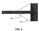
- doping may be performed with a "T" shaped pump electrode 11 having widths W1 and W3 where the diverging regions of ridge 102 are unpumped.
- FIG. 3 shows such a doping configuration with "T" shaped pump electrode 302 that pumps a portion of ridge 102.
- the entire areas of wide region 110 and narrow region 106 are pumped, while only a portion of tapered region 108 is pumped.
- pumping can occur in only a stripe that is the width of narrow region 106 and that extends through tapered region 108 and wide region 110. It should be understood that various pumping configurations may be employed without departing from the scope of the present invention.
- the facet 112 adjacent to narrow region 106 of ridge 102, is perpendicular to the ridge 102 and high reflection coated by deposition of dielectric films, to produce a reflectivity greater than 85%.
- Facet 114 adjacent to wide region 110, is perpendicular to the ridge 102 and low reflection coated by deposition of dielectric films, to produce a reflectivity below 20% and preferably below 15%, for example, around 9%.
- a cavity is thus defined by high-reflection facet 112 (the "rear facet") and low-reflection facet 114 (the "front facet").
- the light-guiding section is the result of the presence of the ridge 102, which induces a variation in the effective refractive-index profile in the lateral direction.
- the effective refractive-index profile is higher in a region under ridge 102 itself and lower in the remaining regions.
- Such effect is known as the index-guiding mechanism.
- the laser light is substantially confined in a region under ridge 102.
- the amount of residual RES defining the depth of the ridge 102, is chosen in order to obtain a refractive-index step suitable for having single-mode operation of the laser in the transverse direction.
- pumping by current injection results in gain-guiding.
- the output facet of the laser is front facet 114, adjacent to the wider region 110.
- the emission wavelength of the laser is preferably around 980 nm.
- the invention laser can be adapted so as to achieve emission at a different wavelength, for example, around 1480 nm.
- Laser 100 is pigtailed by coupling it to a single-mode fiber (not shown in FIG. 1).
- a cylindrical corrective lens is formed, for compensating divergence, only in the vertical direction.
- the width W3 of the third region 110 of the ridge 102 should be similar to the mode field diameter (MFD) of the single-mode fiber.
- MFD mode field diameter
- fibers that are single mode at the emission wavelength are used for coupling with the laser.
- W3 is selected in a range between about 5 and 20 ⁇ m.
- the value of W3 is preferably chosen in a range defined by MFD ⁇ 40% MFD. More preferably, W3 is chosen in a range defined by MFD ⁇ 15% MFD.
- single mode fibers having an MFD value around 8-8.5 ⁇ m can be advantageously used.
- the value of W3 is preferably chosen between about 5 and 11 ⁇ m, more preferably between about 7 and 9 ⁇ m.
- FIG. 4 schematically shows the ridge 102, with geometrical parameters involved together with the longitudinal (Z) and lateral (X) directions.
- the three regions 106, 108, and 110 have different roles, and Applicant has found that their geometrical dimensions have to be carefully determined in order to obtain lasing at high power without degradation of the electro-optic performances of the structure, as explained below.
- High power is considered generally to be greater than about 100 mW.
- First region 106 provides single mode selection in lateral direction during operation of the laser, thus, first region 106 is referred to as a "single-mode region.”
- Single-mode operation of the laser is firstly controlled by the depth of the ridge 102.
- higher order modes can be triggered during oscillations of the laser light in the cavity, and the propagation of such higher order modes has to be avoided in order to have the maximum coupling of energy into the single-mode fiber coupled to the laser.
- single-mode region 106 has to be sufficiently narrow and sufficiently long in order to effectively eliminate higher order modes, that is, in order to act as an effective modal filter.
- the width of the single mode region 106 should be sufficient to provide a good ohmic contact and a reasonably low current density.
- the width W1 of the single mode region 106 may be preferably chosen in a range comprised between 3 and 5 ⁇ m for the preferred emission wavelength range considered.
- Diverging region 108 provides a widening and amplification of the single mode propagating in the cavity, so that the power density along the cavity toward the output facet is lowered while increasing the overall optical power.
- the widening has to be obtained adiabatically, that is, without coupling energy into higher order modes.
- the adiabatic condition limits the angle of divergence ⁇ of the diverging region 108, which depends on the lateral dimensions of the propagating mode, to very small values.
- Diverging region 108 can be referred to as an "adiabatic region.”
- angles lower than about 2.5° are preferred. More preferably, the angle ⁇ is lower than about 1.5°. Even more preferably, the angle ⁇ is lower than 1°.
- the sides of the diverging region 108 can be accomplished in other ways, different from the straight sides shown in fig.4, provided that the divergence has to be performed adiabatically.
- the length of the diverging region 108 is preferably greater than 100 ⁇ m.
- W3 is preferably in a range between 5 and 11 ⁇ m. More preferably, it is in a range between 7 and 9 ⁇ m.
- a first advantage is that the process of manufacturing is facilitated.
- the laser can be produced starting from a long chip 500 or 502, on which at least two devices can be formed. Then, a cleaving action can be performed in order to separate the two lasers.
- chip 500 does not have a wide parallel region but two flared regions that merge, then cleaving must be precise to ensure operable devices. For instance, if the cleaving for chip 500 is not precisely at the merger of the two flared regions, then section (1) may be useable, but section (2) has an unacceptable geometry much different from its mate.
- long chip 502 has a wide parallel region, on the other hand, cleaving permits higher tolerances, thus incrementing the production yield. The same inaccurate cleaving for the embodiment of the invention using long chip 502 leads to slightly different devices (3) and (4), but with substantially the same characteristics.
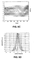
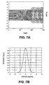
- FIGS. 6A-D and 7A-D report the results of computer simulations on various configurations of ridge lasers.
- the results reported in FIG. 6A-D were obtained with a total cavity length L of 750 ⁇ m, a length L2 of the diverging region 108 of 200 ⁇ m, a refractive index step in the light-guiding section of 0.003 and pumping current of 350 mA.
- the width W1 of the single mode region was 4.6 ⁇ m, while the maximum width of the wide region W3 was 9 ⁇ m.
- FIGS. 6A and 6C show the contour plot of the electromagnetic field in the plane in the GRIN region, obtained with a length L1 of the single mode region respectively of 400 ⁇ m and 200 ⁇ m.
- FIG. 6B a stable profile can be observed, while in FIG. 6D undesirable oscillations are shown, due to poor mode selection and corresponding coupling of energy on higher order modes.
- FIG. 7A-D The results of FIG. 7A-D were obtained with a total cavity length L of 1500 ⁇ m, a length of the tapered region L2 of 200 ⁇ m, a refractive index step in the light-guiding section of 0.003 and a pumping current of 650 mA.
- the width W1 of the single mode region was 4.6 ⁇ m, while the maximum width of the wide region W3 was 9 ⁇ m.
- FIGS. 7A and 7B plot the results obtained with a length L1 of the single mode region of 900 ⁇ m, respectively in the plane of the GRIN region and in the lateral direction on the output facet. As it can be seen, a very stable lasing action is obtained.
- FIGS. 1A and 7B plot the results obtained with a length L1 of the single mode region of 900 ⁇ m, respectively in the plane of the GRIN region and in the lateral direction on the output facet. As it can be seen, a very stable lasing action is obtained.
- the length L1 should be less than about 0.8 L.
- the preferred embodiment of the invention has a larger cross-sectional area (e.g. (3) and (4) in FIG. 5) compared with a device in which the adiabatic region ends at the output facet (e.g. (1) in FIG. 5).
- the electrical resistance is reduced in the device of the present invention.
- the thermal resistance is reduced in the preferred device that has a wide parallel region 110 following adiabatic region 108 in ridge 102.
- a lower thermal resistance leads to a lower operating temperature.
- a lower operating temperature is advantageous, since a corresponding lower enhancement of the refractive index profile in the lateral direction induced by temperature effect can be obtained, leading to a lower probability of triggering higher order modes when high powers are involved.
- a lower operating temperature results in higher reliability of the device. Applicant has found that the laser of the present invention unexpectedly enhances the beneficial effect of a lower operating temperature, due to the presence of the wide parallel region 110 adjacent to the output facet 114.
- FIGS. 8 and 9 report the results of simulations carried out for three kinds of lasers, assuming different geometrical designs of the ridge: (a) a laser having a conventional structure with no diverging regions in the ridge; (b) a laser having a conventional structure with a wide region of an adiabatic region ending at the output facet; and (c) a laser according to the present invention with a wide region of an adiabatic region and a wide parallel region adjacent to the output facet.
- the vertical structure was the same for the three lasers, as well as the ridge depth, the output power and the device length.
- the width W1 of the single mode region (for laser (a) such a width corresponds to the full ridge width) was 4.6 ⁇ m.
- the same length L1 of the single-mode region was used for the lasers (b) and (c).
- FIG. 8A plots the temperature profile within the active layer for the three lasers (with respect to the temperature of a Peltier cell placed below the laser itself, which corresponds to the temperature of the substrate 204) in the lateral direction X (see FIG. 4) at the output facet.
- FIG. 8B plots the temperature profile within the active layer in the longitudinal direction Z (see FIG. 4) along the cavity.
- both lasers (b) and (c) have a larger profile compared to the profile of laser (a) due to the lower power density. Nevertheless, laser (b) has substantially the same temperature enhancement of laser (a), while laser (c) has a much lower peak. It should be noticed that the reduction amount is 25%. This substantial reduction of the temperature allows high power operation without excitation of higher order modes, as previously said.
- both lasers (b) and (c) have a lower profile with respect to laser (a), but laser (c) has the lowest temperature along the whole cavity, with a significant reduction.
- the temperature along the cavity in the Z direction is particularly lower in the region adjacent to the output facet.
- FIGS. 9A-9B are plots of the corresponding data of FIGS. 8A-8B, obtained with a total length of the device of 1500 ⁇ m.
- Table 2 summarizes the geometrical dimensions of the various regions.
- FIGS. 9A-9B are the plots of the peak power profile along the cavity for the same lasers of FIGS. 9A and 9B.
- the advantageous effect of wide parallel region 110 adjacent to the output facet for sample laser (c) is evident for obtaining a lower peak power density.
- the advantageous results on the temperature profile and on the peak power profile are due to the appropriate choice of putting the wide parallel region adjacent to the output facet of the laser, that is in a region where the power is high.
- Such results are significant for a high-power single-mode laser having a spot size with a small lateral dimension.
- This type of laser permits efficient connection by butt-coupling in lateral direction to a single mode fiber.
- the effects on the temperature profile and on the peak power profile are mitigated by the fact that the power density is lower, due to the larger spot size area.
- the length L3 of the wide parallel region adjacent to the output facet should preferably be at least 20 ⁇ m for an appreciable effect from the present invention.
- the length L3 of the wide parallel region should be at least 0.04 L. More preferably, the length L3 of the wide parallel region should be at least 0.1 L. Even more preferably, the length L3 of the wide parallel region should be at least 0.2 L.
- Reliability data collected on more than 300 flared devices according to the invention, having a total length of 750 ⁇ m, tested at different conditions (output power ranging from 200 mW to 350 mW, case temperature from 25 C to 70 C, emission wavelength about 980 nm), indicated that a flared structure according to the invention allows to achieve a failure rate (in FIT units) which is more than 40% lower than the value obtained with a conventional laser having the same cavity length L and no flared structure, operating at the same conditions (output power, case temperature).
- This result is particularly significant for applications for which reliability is a key issue of the component (e.g. submarine applications).
- FIG. 11 shows a plot of the beam intensity profile at the output facet.
- the beam intensity profile 1102 is lower and wider for the laser according to the present invention. This leads to a respective lowering of the power density at the output facet, which is advantageous for avoiding catastrophic optical mirror damage (COMD) when high powers are involved.
- COMP catastrophic optical mirror damage
- FIG. 12 is a plot of the phase profile of the beam at the output facet of the lasers discussed for FIG. 11.
- the phase profile 1202 of the beam for the laser of the invention continuously line
- the phase profile 1204 dashed line
- the laser according to the invention is less astigmatic. This aspect is significant, since a less astigmatic beam allows a more efficient coupling of the power into a fiber, which eliminates the need for additional optics at the coupling.
- a semiconductor laser element as herein described can be typically used as a pump laser for erbium doped optical fiber amplifiers or lasers.
- the skilled in the art can achieve high power laser emission at other specific wavelengths, to provide a pump source for active fibers doped with other rare earth elements.
- the described laser allows to improve existing optical fiber amplifiers in that it allows to increase the amplifier gain and/or its output power which allows, among others, to increase the number of channels that can be amplified.
- the invention laser has a high reliability and this makes the laser particularly advantageous for use in pumping submarine optical amplifiers.
- an optical amplifier typically includes one or more pump lasers and one or more erbium doped active fibers or, in general, rare earth doped active fibers.
- the pump laser or lasers are coupled to the active fiber or fibers by one or more dichroic couplers, e.g., fused fiber couplers or microoptics couplers.
- An optical amplifier for use in a submarine telecommunication system is typically enclosed in a tight, water-proof container.
- a stripe laser using the gain guiding mechanism may be accomplished having the geometrical structure of the guiding section according to the above description.
- a semiconductor amplifier can be realized with a geometrical structure as above described, by providing the facets with antireflection (AR) coatings.
- AR antireflection
- both facet are preferably pigtailed with optical fibers.
- oblique facets i.e., not perpendicular to the ridge
Landscapes
- Physics & Mathematics (AREA)
- Condensed Matter Physics & Semiconductors (AREA)
- General Physics & Mathematics (AREA)
- Electromagnetism (AREA)
- Optics & Photonics (AREA)
- Semiconductor Lasers (AREA)
- Lasers (AREA)
Claims (22)
- Halbleiterelement zum Emittieren eines Einzelmodenlaserlichts bei einer Leistung über 100 mW, welches einen lichtleitenden Abschnitt der Länge L aufweist, welcher der Länge nach zwischen einer hinteren Facette (112) und einer vorderen Facette (114) verläuft, wobei der lichtleitende Abschnitt Folgendes enthält:dadurch gekennzeichnet, dass:einen an die hintere Facette angrenzenden, schmalen Abschnitt (106) mit Seiten, deren relative Divergenz weniger als 0,1° beträgt, der Breite W1 und der Länge L1 zum Leiten eines Singlemode (Einzelmode) der Ausbreitung,einen divergierenden Abschnitt (108) der Länge L2, welcher von einer Breite W1 zu einer Breite W3 breiter wird, zum adiabatischen Erweitern des Singlemode der Ausbreitung,die Länge L1 mehr als 0,4 L beträgt,der lichtleitende Abschnitt einen an die vordere Facette (114) angrenzenden, breiten Abschnitt (110) mit Seiten Breite W3, deren relative Divergenz weniger als 0,1° beträgt, und der Länge L3 enthält, welche mehr als 20 µm beträgt, wobei die Breite W3 in einem Bereich zwischen 5 und 20 µm liegt.
- Halbleiterelement nach Anspruch 1, dadurch gekennzeichnet, dass die hintere Facette (112) mit einer stark reflektierenden Beschichtung und die vordere Facette (114) mit einer gering reflektierenden Beschichtung beschichtet ist.
- Halbleiterelement nach Anspruch 1, dadurch gekennzeichnet, dass beide Facetten (112, 114) mit einer Antireflexionsbeschichtung beschichtet sind.
- Halbleiterelement nach einem der vorangehenden Ansprüche, dadurch gekennzeichnet, dass die Wellenlänge des emittierten Laserlichts ca. 980 nm beträgt.
- Halbleiterelement nach einem der vorangehenden Ansprüche, dadurch gekennzeichnet, dass W3 zwischen 5 und 11 µm umfasst.
- Halbleiterelement nach einem der vorangehenden Ansprüche, dadurch gekennzeichnet, dass W1 zwischen 3 und 5 µm umfasst.
- Halbleiterelement nach einem der vorangehenden Ansprüche, dadurch gekennzeichnet, dass L3 mindestens 0,04 L beträgt.
- Halbleiterelement nach einem der vorangehenden Ansprüche 1-6, dadurch gekennzeichnet, dass L3 mindestens 0,1 L beträgt.
- Halbleiterelement nach einem der vorangehenden Ansprüche, dadurch gekennzeichnet, dass L1 weniger als 0,8 L beträgt.
- Halbleiterelement nach einem der vorangehenden Ansprüche 1 bis 9, dadurch gekennzeichnet, dass L2 mehr als 100 µm beträgt.
- Halbleiterelement nach einem der vorangehenden Ansprüche, dadurch gekennzeichnet, dass der divergierende Abschnitt (108) gerade Seiten mit einem Divergenzwinkel von weniger als 2,5° aufweist.
- Halbleiterelement nach einem der vorangehenden Ansprüche 1-3, dadurch gekennzeichnet, dass die Wellenlänge des emittierten Laserlicht ca. 1480 nm beträgt.
- Halbleiterelement nach einem der vorangehenden Ansprüche, dadurch gekennzeichnet, dass es eine Vielzahl an Schichten in einer vertikalen Richtung enthält.
- Halbleiterelement nach Anspruch 13, dadurch gekennzeichnet, dass ein Steg (102) auf mindestens einer der oberen Schichten der Vielzahl an Schichten definiert ist und dadurch den lichtleitenden Abschnitt definiert.
- Halbleiterelement nach Anspruch 13 oder 14, dadurch gekennzeichnet, dass es
eine aktive Schicht (200a) mit einer Ober- und Unterseite,
eine Kernschicht (200b, 200b') über der Ober- und Unterseite der aktiven Schicht mit einem Brechungsindex n, wobei n mit der Entfernung von der aktiven Schicht abnimmt,
eine Mantelschicht (202, 202') über jeder Kernschicht,
eine obere, dünne Schicht (206) auf einer Mantelschicht und
eine Substratschicht (204) auf der anderen Mantelschicht enthält. - Halbleiterelement nach Anspruch 14, dadurch gekennzeichnet, dass es eine über der Oberfläche des Stegs (102) definierte Pumpenelektrode enthält.
- Halbleiterelement nach Anspruch 16, dadurch gekennzeichnet, dass die Pumpenelektrode über der Gesamtoberfläche des Stegs definiert ist.
- Halbleiterelement nach Anspruch 16, dadurch gekennzeichnet, dass die Pumpenelektrode T-förmig ist und eine Breite W1 über dem schmalen und divergierenden Abschnitt des lichtleitenden Abschnitts und eine Breite W3 über dem breiten Abschnitt des lichtleitenden Abschnitts aufweist.
- Mit einer Anschlusslitze versehenes Halbleiterelement, dadurch gekennzeichnet, dass das optische Halbleiterelement nach einem der vorangehenden Ansprüche an eine Einzelmodenfaser mit einem Modenfelddurchmesser MFD verbunden ist, und dass die Breite W3 in einem Bereich zwischen 0,6 MFD und 1,4 MFD liegt.
- Mit einer Anschlusslitze versehenes Halbleiterelement nach Anspruch 19, dadurch gekennzeichnet, dass die Verbindung mit der Einzelmodenfaser eine Stumpfverbindung ist.
- Glasfaserverstärker, welcher einen mit einer Seltenerde dotierten Glasfaserleiter, ein mit einer Anschlusslitze versehenes Halbleiterelement nach Anspruch 19 zum Schaffen einer Pumpenemission und einen frequenzselektiven Koppler aufweist, welcher zum Koppeln der Pumpenemission mit dem mit einer Seltenerde dotierten Glasfaserleiter geeignet ist.
- Glasfaserverstärker nach Anspruch 21, dadurch gekennzeichnet, dass er weiter einen wasserdichten Behälter enthält, wobei der mit einer Seltenerde dotierte Glasfaserleiter, das mit einer Anschlusslitze versehene Halbleiterelement und der frequenzselektive Koppler vom Behälter umgeben sind.
Priority Applications (1)
| Application Number | Priority Date | Filing Date | Title |
|---|---|---|---|
| EP00990008A EP1243055B1 (de) | 1999-12-27 | 2000-12-20 | Halbleiterlaservorrichtung mit einer divergierenden region |
Applications Claiming Priority (6)
| Application Number | Priority Date | Filing Date | Title |
|---|---|---|---|
| EP99126003 | 1999-12-27 | ||
| EP99126003 | 1999-12-27 | ||
| US17735300P | 2000-01-24 | 2000-01-24 | |
| US177353P | 2000-01-24 | ||
| EP00990008A EP1243055B1 (de) | 1999-12-27 | 2000-12-20 | Halbleiterlaservorrichtung mit einer divergierenden region |
| PCT/EP2000/013057 WO2001048874A2 (en) | 1999-12-27 | 2000-12-20 | Semiconductor laser element having a diverging region |
Publications (2)
| Publication Number | Publication Date |
|---|---|
| EP1243055A2 EP1243055A2 (de) | 2002-09-25 |
| EP1243055B1 true EP1243055B1 (de) | 2004-10-13 |
Family
ID=56290092
Family Applications (1)
| Application Number | Title | Priority Date | Filing Date |
|---|---|---|---|
| EP00990008A Expired - Lifetime EP1243055B1 (de) | 1999-12-27 | 2000-12-20 | Halbleiterlaservorrichtung mit einer divergierenden region |
Country Status (7)
| Country | Link |
|---|---|
| EP (1) | EP1243055B1 (de) |
| JP (1) | JP2003518777A (de) |
| CN (1) | CN1415128A (de) |
| AU (1) | AU770757B2 (de) |
| CA (1) | CA2395309A1 (de) |
| DE (1) | DE60014969T2 (de) |
| WO (1) | WO2001048874A2 (de) |
Families Citing this family (24)
| Publication number | Priority date | Publication date | Assignee | Title |
|---|---|---|---|---|
| US6816531B1 (en) * | 2000-03-03 | 2004-11-09 | Jds Uniphase Corporation | High-power, kink-free, single mode laser diodes |
| JP5261857B2 (ja) * | 2001-09-21 | 2013-08-14 | 日本電気株式会社 | 端面発光型半導体レーザおよび半導体レーザ・モジュール |
| IES20030516A2 (en) * | 2003-07-11 | 2004-10-06 | Eblana Photonics Ltd | Semiconductor laser and method of manufacture |
| JP4751024B2 (ja) * | 2004-01-16 | 2011-08-17 | シャープ株式会社 | 半導体レーザおよびその製造方法 |
| JP2005209952A (ja) * | 2004-01-23 | 2005-08-04 | Matsushita Electric Ind Co Ltd | 半導体レーザ装置およびそれを用いた光ピックアップ装置 |
| JP5005300B2 (ja) * | 2006-09-07 | 2012-08-22 | パナソニック株式会社 | 半導体レーザ装置 |
| DE102007026925A1 (de) * | 2007-02-28 | 2008-09-04 | Osram Opto Semiconductors Gmbh | Integrierte Trapezlaseranordnung und Verfahren zu deren Herstellung |
| JP2009033009A (ja) * | 2007-07-30 | 2009-02-12 | Panasonic Corp | 半導体レーザ装置及びその製造方法 |
| DE102008014093B4 (de) * | 2007-12-27 | 2020-02-06 | Osram Opto Semiconductors Gmbh | Kantenemittierender Halbleiterlaserchip mit zumindest einer Strombarriere |
| JP5913878B2 (ja) * | 2011-09-20 | 2016-04-27 | 日本オクラロ株式会社 | 半導体レーザ素子、それを備える光送信モジュール、光トランシーバ、及び半導体レーザ素子の製造方法 |
| US9214786B2 (en) | 2013-04-09 | 2015-12-15 | Nlight Photonics Corporation | Diode laser packages with flared laser oscillator waveguides |
| US9166369B2 (en) * | 2013-04-09 | 2015-10-20 | Nlight Photonics Corporation | Flared laser oscillator waveguide |
| US10186836B2 (en) | 2014-10-10 | 2019-01-22 | Nlight, Inc. | Multiple flared laser oscillator waveguide |
| CN104269739B (zh) * | 2014-10-20 | 2017-03-22 | 中国电子科技集团公司第四十四研究所 | 一种低成本大功率半导体基横模激光器芯片结构 |
| WO2016197137A1 (en) | 2015-06-04 | 2016-12-08 | Nlight, Inc. | Angled dbr-grating laser/amplifier with one or more mode-hopping regions |
| DE102015119226A1 (de) * | 2015-11-09 | 2017-05-11 | Osram Opto Semiconductors Gmbh | Halbleiterlaserdiode |
| CN105633795A (zh) * | 2016-03-28 | 2016-06-01 | 长春理工大学 | 一种扩展透明窗口半导体激光器 |
| JP6717733B2 (ja) * | 2016-11-04 | 2020-07-01 | 日本電信電話株式会社 | 半導体光集積回路 |
| CN106911078A (zh) * | 2017-02-17 | 2017-06-30 | 武汉光安伦光电技术有限公司 | 小发散角脊型激光器及其制作方法 |
| CN108963754B (zh) * | 2018-07-02 | 2020-10-16 | 福建中科光芯光电科技有限公司 | 一种光通信波段低发散角dfb半导体激光器的制备方法 |
| US11837838B1 (en) * | 2020-01-31 | 2023-12-05 | Freedom Photonics Llc | Laser having tapered region |
| EP4352839A4 (de) | 2021-06-10 | 2025-05-07 | Freedom Photonics LLC | Entwürfe für laterale stromsteuerung in optischen verstärkern und lasern |
| CN115332940B (zh) * | 2022-10-11 | 2022-12-13 | 苏州长光华芯光电技术股份有限公司 | 侧向光模式调节高功率半导体器件及其制备方法 |
| CN120601248B (zh) * | 2025-08-07 | 2025-09-26 | 华辰芯光(无锡)半导体有限公司 | 一种单模高功率边发射激光器及制备方法 |
Family Cites Families (4)
| Publication number | Priority date | Publication date | Assignee | Title |
|---|---|---|---|---|
| US4349905A (en) * | 1980-07-22 | 1982-09-14 | Hewlett-Packard Company | Tapered stripe semiconductor laser |
| JPS6120913A (ja) * | 1984-07-10 | 1986-01-29 | Matsushita Electric Ind Co Ltd | Ld光伝送装置 |
| US4942585A (en) * | 1987-12-22 | 1990-07-17 | Ortel Corporation | High power semiconductor laser |
| JP2695440B2 (ja) * | 1988-07-07 | 1997-12-24 | 三菱電機株式会社 | 半導体レーザ装置 |
-
2000
- 2000-12-20 DE DE60014969T patent/DE60014969T2/de not_active Expired - Fee Related
- 2000-12-20 EP EP00990008A patent/EP1243055B1/de not_active Expired - Lifetime
- 2000-12-20 WO PCT/EP2000/013057 patent/WO2001048874A2/en not_active Ceased
- 2000-12-20 CN CN00817842A patent/CN1415128A/zh active Pending
- 2000-12-20 CA CA002395309A patent/CA2395309A1/en not_active Abandoned
- 2000-12-20 JP JP2001548483A patent/JP2003518777A/ja not_active Withdrawn
- 2000-12-20 AU AU26755/01A patent/AU770757B2/en not_active Ceased
Also Published As
| Publication number | Publication date |
|---|---|
| AU770757B2 (en) | 2004-03-04 |
| CN1415128A (zh) | 2003-04-30 |
| CA2395309A1 (en) | 2001-07-05 |
| WO2001048874A3 (en) | 2001-12-13 |
| DE60014969D1 (de) | 2004-11-18 |
| DE60014969T2 (de) | 2005-10-13 |
| AU2675501A (en) | 2001-07-09 |
| WO2001048874A2 (en) | 2001-07-05 |
| EP1243055A2 (de) | 2002-09-25 |
| JP2003518777A (ja) | 2003-06-10 |
Similar Documents
| Publication | Publication Date | Title |
|---|---|---|
| EP1243055B1 (de) | Halbleiterlaservorrichtung mit einer divergierenden region | |
| US6826220B2 (en) | Semiconductor laser element having a diverging region | |
| US4783788A (en) | High power semiconductor lasers | |
| US6625182B1 (en) | Semiconductor or solid-state laser having an external fiber cavity | |
| US4856017A (en) | Single frequency high power semiconductor laser | |
| JP5261857B2 (ja) | 端面発光型半導体レーザおよび半導体レーザ・モジュール | |
| EP1121720B1 (de) | Hochleistungshalbleiterlichtquelle | |
| US6445724B2 (en) | Master oscillator vertical emission laser | |
| US6167073A (en) | High power laterally antiguided semiconductor light source with reduced transverse optical confinement | |
| US5349602A (en) | Broad-area MOPA device with leaky waveguide beam expander | |
| US5272711A (en) | High-power semiconductor laser diode | |
| US7127145B2 (en) | Semiconductor optical amplifier, and optical module using the same | |
| US6714574B2 (en) | Monolithically integrated optically-pumped edge-emitting semiconductor laser | |
| US6750478B2 (en) | Semiconductor laser device and method for suppressing fabry perot oscillations | |
| JP2005524234A (ja) | 高出力半導体レーザ・ダイオードおよびそのようなダイオードの製造方法 | |
| US6477191B1 (en) | Semiconductor laser device, semiconductor laser module, rare-earth-element-doped optical fiber amplifier and fiber laser | |
| JPH08330671A (ja) | 半導体光素子 | |
| US4348763A (en) | Multiple stripe leaky mode laser | |
| CA1252188A (en) | Single mode injection laser structure | |
| US6137625A (en) | Semiconductor optical amplifier and integrated laser source information | |
| JPH10163563A (ja) | 半導体レーザ | |
| WO2021148120A1 (en) | Single-mode dfb laser | |
| JP2000357841A (ja) | 半導体レーザ素子、半導体レーザモジュール、希土類添加光ファイバ増幅器、およびファイバレーザ | |
| JP2967757B2 (ja) | 半導体レーザ装置及びその製造方法 | |
| JP4309636B2 (ja) | 半導体レーザおよび光通信用素子 |
Legal Events
| Date | Code | Title | Description |
|---|---|---|---|
| PUAI | Public reference made under article 153(3) epc to a published international application that has entered the european phase |
Free format text: ORIGINAL CODE: 0009012 |
|
| 17P | Request for examination filed |
Effective date: 20020617 |
|
| AK | Designated contracting states |
Kind code of ref document: A2 Designated state(s): AT BE CH CY DE DK ES FI FR GB GR IE IT LI LU MC NL PT SE TR |
|
| AX | Request for extension of the european patent |
Free format text: AL;LT;LV;MK;RO;SI |
|
| 17Q | First examination report despatched |
Effective date: 20030318 |
|
| RAP1 | Party data changed (applicant data changed or rights of an application transferred) |
Owner name: CORNING O.T.I. S.P.A. |
|
| GRAP | Despatch of communication of intention to grant a patent |
Free format text: ORIGINAL CODE: EPIDOSNIGR1 |
|
| RBV | Designated contracting states (corrected) |
Designated state(s): DE FR GB IT |
|
| GRAS | Grant fee paid |
Free format text: ORIGINAL CODE: EPIDOSNIGR3 |
|
| GRAA | (expected) grant |
Free format text: ORIGINAL CODE: 0009210 |
|
| RAP1 | Party data changed (applicant data changed or rights of an application transferred) |
Owner name: CORNING O.T.I. S.R.L |
|
| AK | Designated contracting states |
Kind code of ref document: B1 Designated state(s): DE FR GB IT |
|
| REG | Reference to a national code |
Ref country code: GB Ref legal event code: FG4D |
|
| REG | Reference to a national code |
Ref country code: IE Ref legal event code: FG4D |
|
| REF | Corresponds to: |
Ref document number: 60014969 Country of ref document: DE Date of ref document: 20041118 Kind code of ref document: P |
|
| LTIE | Lt: invalidation of european patent or patent extension |
Effective date: 20041013 |
|
| PLBE | No opposition filed within time limit |
Free format text: ORIGINAL CODE: 0009261 |
|
| STAA | Information on the status of an ep patent application or granted ep patent |
Free format text: STATUS: NO OPPOSITION FILED WITHIN TIME LIMIT |
|
| ET | Fr: translation filed | ||
| 26N | No opposition filed |
Effective date: 20050714 |
|
| PGFP | Annual fee paid to national office [announced via postgrant information from national office to epo] |
Ref country code: FR Payment date: 20061220 Year of fee payment: 7 |
|
| PGFP | Annual fee paid to national office [announced via postgrant information from national office to epo] |
Ref country code: GB Payment date: 20061222 Year of fee payment: 7 |
|
| PGFP | Annual fee paid to national office [announced via postgrant information from national office to epo] |
Ref country code: IT Payment date: 20061231 Year of fee payment: 7 |
|
| PGFP | Annual fee paid to national office [announced via postgrant information from national office to epo] |
Ref country code: DE Payment date: 20070131 Year of fee payment: 7 |
|
| GBPC | Gb: european patent ceased through non-payment of renewal fee |
Effective date: 20071220 |
|
| PG25 | Lapsed in a contracting state [announced via postgrant information from national office to epo] |
Ref country code: DE Free format text: LAPSE BECAUSE OF NON-PAYMENT OF DUE FEES Effective date: 20080701 |
|
| REG | Reference to a national code |
Ref country code: FR Ref legal event code: ST Effective date: 20081020 |
|
| PG25 | Lapsed in a contracting state [announced via postgrant information from national office to epo] |
Ref country code: GB Free format text: LAPSE BECAUSE OF NON-PAYMENT OF DUE FEES Effective date: 20071220 |
|
| PG25 | Lapsed in a contracting state [announced via postgrant information from national office to epo] |
Ref country code: FR Free format text: LAPSE BECAUSE OF NON-PAYMENT OF DUE FEES Effective date: 20071231 |
|
| PG25 | Lapsed in a contracting state [announced via postgrant information from national office to epo] |
Ref country code: IT Free format text: LAPSE BECAUSE OF NON-PAYMENT OF DUE FEES Effective date: 20071220 |