EP1246160A2 - Steuerverfahren für Flüssigkristallanzeige mit aktiver Matrix - Google Patents
Steuerverfahren für Flüssigkristallanzeige mit aktiver Matrix Download PDFInfo
- Publication number
- EP1246160A2 EP1246160A2 EP02252388A EP02252388A EP1246160A2 EP 1246160 A2 EP1246160 A2 EP 1246160A2 EP 02252388 A EP02252388 A EP 02252388A EP 02252388 A EP02252388 A EP 02252388A EP 1246160 A2 EP1246160 A2 EP 1246160A2
- Authority
- EP
- European Patent Office
- Prior art keywords
- voltage
- opposing electrode
- liquid crystal
- data
- display
- Prior art date
- Legal status (The legal status is an assumption and is not a legal conclusion. Google has not performed a legal analysis and makes no representation as to the accuracy of the status listed.)
- Withdrawn
Links
- 239000004973 liquid crystal related substance Substances 0.000 title claims abstract description 57
- 239000011159 matrix material Substances 0.000 title claims abstract description 26
- 238000000034 method Methods 0.000 title claims description 8
- 230000008859 change Effects 0.000 claims abstract description 48
- 239000000758 substrate Substances 0.000 claims description 28
- 230000015556 catabolic process Effects 0.000 description 5
- 238000006731 degradation reaction Methods 0.000 description 5
- 238000010586 diagram Methods 0.000 description 4
- 230000009467 reduction Effects 0.000 description 4
- 230000004044 response Effects 0.000 description 4
- 101150015395 TAF12B gene Proteins 0.000 description 3
- 239000003990 capacitor Substances 0.000 description 3
- 229920005994 diacetyl cellulose Polymers 0.000 description 3
- 102100027992 Casein kinase II subunit beta Human genes 0.000 description 2
- 101000858625 Homo sapiens Casein kinase II subunit beta Proteins 0.000 description 2
- 238000012937 correction Methods 0.000 description 2
- 230000008878 coupling Effects 0.000 description 2
- 238000010168 coupling process Methods 0.000 description 2
- 238000005859 coupling reaction Methods 0.000 description 2
- 230000003071 parasitic effect Effects 0.000 description 2
- 229910021420 polycrystalline silicon Inorganic materials 0.000 description 2
- 239000010409 thin film Substances 0.000 description 2
- 102100024452 DNA-directed RNA polymerase III subunit RPC1 Human genes 0.000 description 1
- 101000689002 Homo sapiens DNA-directed RNA polymerase III subunit RPC1 Proteins 0.000 description 1
- VYPSYNLAJGMNEJ-UHFFFAOYSA-N Silicium dioxide Chemical group O=[Si]=O VYPSYNLAJGMNEJ-UHFFFAOYSA-N 0.000 description 1
- 230000002411 adverse Effects 0.000 description 1
- 230000003321 amplification Effects 0.000 description 1
- 239000003086 colorant Substances 0.000 description 1
- 239000002131 composite material Substances 0.000 description 1
- 230000007547 defect Effects 0.000 description 1
- 230000000593 degrading effect Effects 0.000 description 1
- 230000000694 effects Effects 0.000 description 1
- 239000011521 glass Substances 0.000 description 1
- 238000003199 nucleic acid amplification method Methods 0.000 description 1
- 230000002688 persistence Effects 0.000 description 1
- 229920005591 polysilicon Polymers 0.000 description 1
- 238000007789 sealing Methods 0.000 description 1
- 230000007704 transition Effects 0.000 description 1
Images


Classifications
-
- G—PHYSICS
- G09—EDUCATION; CRYPTOGRAPHY; DISPLAY; ADVERTISING; SEALS
- G09G—ARRANGEMENTS OR CIRCUITS FOR CONTROL OF INDICATING DEVICES USING STATIC MEANS TO PRESENT VARIABLE INFORMATION
- G09G3/00—Control arrangements or circuits, of interest only in connection with visual indicators other than cathode-ray tubes
- G09G3/20—Control arrangements or circuits, of interest only in connection with visual indicators other than cathode-ray tubes for presentation of an assembly of a number of characters, e.g. a page, by composing the assembly by combination of individual elements arranged in a matrix no fixed position being assigned to or needed to be assigned to the individual characters or partial characters
- G09G3/34—Control arrangements or circuits, of interest only in connection with visual indicators other than cathode-ray tubes for presentation of an assembly of a number of characters, e.g. a page, by composing the assembly by combination of individual elements arranged in a matrix no fixed position being assigned to or needed to be assigned to the individual characters or partial characters by control of light from an independent source
- G09G3/36—Control arrangements or circuits, of interest only in connection with visual indicators other than cathode-ray tubes for presentation of an assembly of a number of characters, e.g. a page, by composing the assembly by combination of individual elements arranged in a matrix no fixed position being assigned to or needed to be assigned to the individual characters or partial characters by control of light from an independent source using liquid crystals
- G09G3/3611—Control of matrices with row and column drivers
- G09G3/3648—Control of matrices with row and column drivers using an active matrix
-
- G—PHYSICS
- G09—EDUCATION; CRYPTOGRAPHY; DISPLAY; ADVERTISING; SEALS
- G09G—ARRANGEMENTS OR CIRCUITS FOR CONTROL OF INDICATING DEVICES USING STATIC MEANS TO PRESENT VARIABLE INFORMATION
- G09G2310/00—Command of the display device
- G09G2310/02—Addressing, scanning or driving the display screen or processing steps related thereto
- G09G2310/0243—Details of the generation of driving signals
- G09G2310/0248—Precharge or discharge of column electrodes before or after applying exact column voltages
-
- G—PHYSICS
- G09—EDUCATION; CRYPTOGRAPHY; DISPLAY; ADVERTISING; SEALS
- G09G—ARRANGEMENTS OR CIRCUITS FOR CONTROL OF INDICATING DEVICES USING STATIC MEANS TO PRESENT VARIABLE INFORMATION
- G09G2320/00—Control of display operating conditions
- G09G2320/02—Improving the quality of display appearance
-
- G—PHYSICS
- G09—EDUCATION; CRYPTOGRAPHY; DISPLAY; ADVERTISING; SEALS
- G09G—ARRANGEMENTS OR CIRCUITS FOR CONTROL OF INDICATING DEVICES USING STATIC MEANS TO PRESENT VARIABLE INFORMATION
- G09G3/00—Control arrangements or circuits, of interest only in connection with visual indicators other than cathode-ray tubes
- G09G3/20—Control arrangements or circuits, of interest only in connection with visual indicators other than cathode-ray tubes for presentation of an assembly of a number of characters, e.g. a page, by composing the assembly by combination of individual elements arranged in a matrix no fixed position being assigned to or needed to be assigned to the individual characters or partial characters
- G09G3/34—Control arrangements or circuits, of interest only in connection with visual indicators other than cathode-ray tubes for presentation of an assembly of a number of characters, e.g. a page, by composing the assembly by combination of individual elements arranged in a matrix no fixed position being assigned to or needed to be assigned to the individual characters or partial characters by control of light from an independent source
- G09G3/36—Control arrangements or circuits, of interest only in connection with visual indicators other than cathode-ray tubes for presentation of an assembly of a number of characters, e.g. a page, by composing the assembly by combination of individual elements arranged in a matrix no fixed position being assigned to or needed to be assigned to the individual characters or partial characters by control of light from an independent source using liquid crystals
- G09G3/3611—Control of matrices with row and column drivers
- G09G3/3614—Control of polarity reversal in general
-
- G—PHYSICS
- G09—EDUCATION; CRYPTOGRAPHY; DISPLAY; ADVERTISING; SEALS
- G09G—ARRANGEMENTS OR CIRCUITS FOR CONTROL OF INDICATING DEVICES USING STATIC MEANS TO PRESENT VARIABLE INFORMATION
- G09G3/00—Control arrangements or circuits, of interest only in connection with visual indicators other than cathode-ray tubes
- G09G3/20—Control arrangements or circuits, of interest only in connection with visual indicators other than cathode-ray tubes for presentation of an assembly of a number of characters, e.g. a page, by composing the assembly by combination of individual elements arranged in a matrix no fixed position being assigned to or needed to be assigned to the individual characters or partial characters
- G09G3/34—Control arrangements or circuits, of interest only in connection with visual indicators other than cathode-ray tubes for presentation of an assembly of a number of characters, e.g. a page, by composing the assembly by combination of individual elements arranged in a matrix no fixed position being assigned to or needed to be assigned to the individual characters or partial characters by control of light from an independent source
- G09G3/36—Control arrangements or circuits, of interest only in connection with visual indicators other than cathode-ray tubes for presentation of an assembly of a number of characters, e.g. a page, by composing the assembly by combination of individual elements arranged in a matrix no fixed position being assigned to or needed to be assigned to the individual characters or partial characters by control of light from an independent source using liquid crystals
- G09G3/3611—Control of matrices with row and column drivers
- G09G3/3648—Control of matrices with row and column drivers using an active matrix
- G09G3/3655—Details of drivers for counter electrodes, e.g. common electrodes for pixel capacitors or supplementary storage capacitors
-
- G—PHYSICS
- G09—EDUCATION; CRYPTOGRAPHY; DISPLAY; ADVERTISING; SEALS
- G09G—ARRANGEMENTS OR CIRCUITS FOR CONTROL OF INDICATING DEVICES USING STATIC MEANS TO PRESENT VARIABLE INFORMATION
- G09G3/00—Control arrangements or circuits, of interest only in connection with visual indicators other than cathode-ray tubes
- G09G3/20—Control arrangements or circuits, of interest only in connection with visual indicators other than cathode-ray tubes for presentation of an assembly of a number of characters, e.g. a page, by composing the assembly by combination of individual elements arranged in a matrix no fixed position being assigned to or needed to be assigned to the individual characters or partial characters
- G09G3/34—Control arrangements or circuits, of interest only in connection with visual indicators other than cathode-ray tubes for presentation of an assembly of a number of characters, e.g. a page, by composing the assembly by combination of individual elements arranged in a matrix no fixed position being assigned to or needed to be assigned to the individual characters or partial characters by control of light from an independent source
- G09G3/36—Control arrangements or circuits, of interest only in connection with visual indicators other than cathode-ray tubes for presentation of an assembly of a number of characters, e.g. a page, by composing the assembly by combination of individual elements arranged in a matrix no fixed position being assigned to or needed to be assigned to the individual characters or partial characters by control of light from an independent source using liquid crystals
- G09G3/3611—Control of matrices with row and column drivers
- G09G3/3685—Details of drivers for data electrodes
- G09G3/3688—Details of drivers for data electrodes suitable for active matrices only
Definitions
- the present invention relates to method of driving an active matrix type liquid crystal display, and more particularly to a method of alternating drive of opposing electrodes in active matrix type liquid crystal displays.
- An active matrix type liquid crystal display comprises a switch element such as a thin film transistor (hereinafter referred to as a "TFT") in each pixel, and display data is supplied to each pixel electrode via the switch element so that the alignment of liquid crystal in each pixel is controlled by the pixel electrode and an opposing electrode (common electrode) provided to oppose the pixel electrode with the liquid crystal in between.
- TFT thin film transistor
- liquid crystal display inherently has a low power consumption, further reduction in the power consumption is strongly demanded in portable information devices or the like to which LCD displays are equipped, and, consequently, still further reduction in the power consumption of liquid crystal displays is desired.
- liquid crystal drive voltage which is applied between the pixel electrode and the opposing electrode can be reduced, power consumption can be reduced.
- application of sufficient voltage to the liquid crystal is desired, and, thus, the applied voltage to the liquid crystal cannot be reduced significantly. Therefore, in a liquid crystal display, there is a need for some means that can reduce the power consumption without reducing the voltage applied to the liquid crystal and without degrading the display quality and reliability of the device.
- the present invention was conceived to solve at least the problem mentioned above, and one object of the present invention is to provide an active matrix type liquid crystal display in which the power consumption is reduced and, at the same time, necessary and sufficient voltage can be applied to the liquid crystals.
- a method for driving an active matrix type liquid crystal display wherein, in the active matrix type liquid crystal display, liquid crystal are sealed in between a first substrate and a second substrate;
- the first substrate comprises switching elements and pixel electrodes connected to the switching elements, both of which are provided in correspondence to pixels that are arranged in a matrix, selection lines for sequentially selecting the switching elements, and data lines for supplying display data to the switching elements that are connected;
- the second substrate comprises an opposing electrode for controlling, along with each of the pixel electrodes on the first electrode, the liquid crystal, the method comprising the steps of periodically changing, in a predetermined period, the opposing electrode voltage which is applied to the opposing electrode, and applying a change alleviating voltage to the data lines when the opposing electrode voltage is changed
- a drive circuit for an active matrix type display wherein, in an active matrix type display, liquid crystal is sealed between a first substrate and a second substrate, the first substrate comprises switching elements and pixel electrodes connected to the switching elements, both of which are provided in correspondence to pixels that are arranged in a matrix, selection lines for sequentially selecting the switching elements, and data lines for supplying display data to the switching elements that are connected, and the second substrate comprises an opposing electrode for controlling, along with each of the pixel electrode on the first substrate, the liquid crystal.
- Such a drive circuit comprises an opposing electrode controller for periodically changing, in a predetermined period, the opposing electrode voltage which is applied to the opposing electrode; and a data line voltage controller for applying a change alleviating voltage onto the data lines during the change in the opposing electrode voltage.
- a constant common voltage Vcom is applied to an opposing electrode and the polarity, with respect to the common voltage Vcom, of display data applied to each pixel electrode is periodically inverted in a predetermined period, to alternately drive the liquid crystals.
- the voltage on the opposing electrode is also periodically changed, that is, alternately driven. Because of this, sufficient voltage can be ensured for application to the liquid crystal without increasing the amplitude of the display data in which the polarity with respect to a predetermined reference isperiodicallyinverted.
- a change alleviating voltage to the data lines during when the opposing electrode voltage is changed, large changes in the potential of the data lines caused by capacity coupling and the change in the opposing electrode potential are both inhibited.
- the data lines formed on the first substrate are, in many cases, laid out to oppose the opposing electrode with the liquid crystals in between. Therefore, in the equivalent circuit, a parasitic capacitance is formed between the data line and the opposing electrode and is connected to the data line, and, in some cases, the potential on the data line may change in response to the change in the opposing electrode voltage when such a change occurs.
- the change in the opposing electrode voltage is executed during the non-selection period of the pixels such as the vertical blanking interval and horizontal blanking interval, but, because no pixel is selected during such these intervals, the data line is electrically separated from the display data source. As result, the potential of the data line tends to change in response to the change in the opposing electrode voltage .
- the change alleviating voltage is at the center voltage of the display data.
- the degradation of the display data output switch can be reliably prevented without increasing the circuit loading.
- the polarity, with respect to the center voltage, of the display data which is output to the data lines is periodically inverted in a predetermined period, no delay in the inversion operation is caused and the display quality is not adversely affected, even if the voltage of the data lines is set at the center voltage when the pixels are not selected.
- the voltage change on the data lines when the opposing electrode voltage is changed is also reduced. Therefore, because unnecessary loading to the switches or the like for selecting a data line can be prevented, the possibility of display defects in the column direction can be reduced, display quality can be maintained, and device reliability can be improved.
- Fig. 1 shows an overall structure of an active matrix type liquid crystal display according to the embodiment of the present invention.
- Fig. 2 shows a structure of a drive IC 100 for a display panel.
- a liquid crystal display panel 200 is constructed by affixing a first substrate and a second substrate, each made of, for example, a glass substrate, with a predetermined gap between them and sealing liquid crystal in this gap.
- pixel electrodes which are arranged in a matrix and switching elements 10 (here a TFT having a double gate structure) respectively connected to the pixel electrodes are formed on the first substrate, and, furthermore, selection lines (gate lines) 12 for sequentially selecting the TFTs and data lines 22 for supplying display data to the selected TFT are provided on the first substrate.
- the pixel electrode formed for each pixel is constituted by a liquid crystal capacitor Clc and an opposing electrode (common electrode) formed on the second substrate with the liquid crystal in between.
- the alignment of the liquid crystal is controlled based on the potential difference (alternating) between the display data voltage which is applied to the pixel electrode via each TFT 10 and the voltage on the opposing electrode, to effect display at each pixel.
- a storage capacitor Csc is provided in parallel to the liquid crystal capacitor Clc and connected to the pixel TFT 10, and maintains the pixel electrode voltage for one display period (one vertical scan period).
- a p-Si TFT which uses polycrystalline silicon (polysilicon, or "p-Si" as the active layer can be used to form not only the switch elements in the pixels, but also the transistors constituting the drivers.
- p-Si TFTs are employed. As shown in Fig. 1, on the first substrate, pixel p-Si TFTs 10, a horizontal direction (H) driver 220, data output switches Hsw for controlling the timing for outputting data from the H driver 220, change alleviating voltage output switches (hereinafter referred to as "alleviating voltage output switch") Msw to be described later, and a vertical direction (V) driver 210 for sequentially outputting selection signals to the gate lines 12 are provided.
- H horizontal direction
- V vertical direction
- a drive IC 100 has a structure as shown in Fig. 2, and produces analog display data (R, G, and B data for color display), various timing signals for driving the V driver 210 and the H driver 220, opposing electrode voltage signal Vcom, etc., and outputs these to the liquid crystal display panel 200.
- a serial to parallel converter circuit 102 converts serially input signals such as, for example, 8-bit digital videosignalsintoparalleldata.
- An RGB matrix circuit 104 reproduces digital data of R, G, and B primary colors from the composite digital video data supplied from the converter circuit 102.
- a sample/hold circuit 106 samples the R, G, and B data and a correction circuit 108 applies contrast, brightness, and gamma corrections to each of the R, G, and B data streams and outputs each to a respective corresponding digital to analog converter circuit (DAC) 110 among a plurality of DACs 110.
- the R, G, and B video signals converted to analog signals at the DACs 110 are respectively amplified by one of a plurality of operational amplifiers 112, and are output to the video lines of the panel 200 as analog R, G, and B display data.
- the drive IC 100 further comprises a CPU interface (I/F) circuit 120 and a timing controller (T/C) 160, and in some cases further comprises a built-in VCO 180.
- the T/C 160 produces and supplies a change alleviation control signal Mc to be described later and panel control signals (timings signals) necessary for operation of the V driver 210 and H driver 220 shown in Fig. 1, using a clock from the VCO 180 and based on the timing signals such as a master clock MCLK, a horizontal synchronization signal Hsync, and a vertical synchronizationsignalVsync.
- the T/C160 produces and supplies timing signals necessary for each of the circuits for video signal processing system as described above .
- the T/C 160 forms an opposing electrode controller, and generates a Vcom inversion control signal COM-FRP for periodically inverting the opposing electrode voltage signal (Vcom) in a predetermined period and outputs COM-FRP to an analog switch 140 to be described below.
- Vcom opposing electrode voltage signal
- the I/F circuit 120 receives and interprets instructions transmitted from a CPU (not shown) , and outputs an opposing electrode driving signal (Vcom) and a change alleviating voltage signal (VM) which are both digital signals .
- a DAC 122 converts the digital change alleviating voltage signal into an analog signal and outputs the converted analog signal to the display panel 200 after amplification by an operational amplifier 124.
- Digital opposing electrode voltage signals which are output from the I/F circuit 120 and have opposite polarities are respectively converted to analog signals by DACs 130 and 134, and amplified by a first operational amplifier 132 and a second operational amplifier 136.
- the analog switch 140 Based on the Vcom inversion control signal from the T/C 160, the analog switch 140 alternately selects one of the first and second operational amplifiers 132 and 136. Inthismanner, the output from the selected one of the amplifiers 132 and 136 is supplied to the Vcom output terminal.
- Fig. 3 shows a relationship between the display data signal waveform on the data line and the voltage waveform on the opposing electrode.
- the V driver 210 and H driver 220 shown in Fig. 1 are controlled, pixel TFTs 10 are sequentially selected in row units, and the display data signal which is output on the corresponding data line is applied to the pixel electrode via the selected TFT 10.
- the liquid crystal In order to prevent persistence, the liquid crystal must be alternately driven by periodically inverting the polarity of the applied voltage in a predetermined period.
- a so-called line inversion drive is employed in which the voltage level of the display data is inverted every horizontal scan period (1H). Furthermore in the subsequent frame, an opposite polarity is applied on the same line. With such line inversion drive, the potential at a predetermined position changes on a data line changes as shown in Fig. 3, and the polarity of the display data is inverted with respect to a video center voltage Vc every 1H.
- the opposing electrode voltage (Vcom) is also periodically inverted.
- liquid crystal is driven by a potential difference between the potential of the opposing electrode and the potential of the display data which are written to each of the pixel electrodes.
- the opposing electrode voltage is fixed at a video center voltage Vc, but by inverting the opposing electrode potential, for example, every 1H, similar as for the display data, it is possible to apply the same voltage to the liquid crystal as when the opposing electrode voltage is fixed at Vc, even when the amplitude of the display data signal is reduced. This configuration is therefore useful in view of reduction in the power consumption of the device.
- Such inversion of the opposing electrode voltage is performed during a non-display period, such as the horizontal blanking interval within one horizontal scan period or the vertical blanking interval within one vertical scan period.
- the reference voltage for the inversion is the center voltage Vrc of the voltage which is actually applied to the liquid crystal.
- the outputs from the V driver 210 and form the H driver 220 are stopped.
- Data output switches Hsw are provided between the H driver 220 and the data lines 22, and these switches are controlled to be switched off during the non-display period. Therefore, during the non-display period, all data lines 22 are electrically separated.
- the data lines 22 are formed on the first substrate to align with the pixel electrodes, and, in many cases, parasitic capacitances are created between the data lines 22 and the opposing electrode on the second substrate, with the liquid crystal in between. Therefore, if the opposing electrode voltage Vcom is inverted when these data lines 22 are electrically separated, capacity coupling is generated and the potentials of the data lines 22 tend to change in response to the opposing electrode voltage.
- the waveforms (a) and (b) as shown in Fig. 3 illustrate the potential of a data line 22 which is changed in response to the change in the opposing electrode voltage. For example, if the amplitude of inversion of the opposing electrode voltage is 3.5 V, when the opposing electrode voltage is reduced, the potential at the data line 22 is rapidly reduced by 3.5 V. In contrast, when the opposing electrode voltage is increased, the potential of the data line 22 is also increased by 3.5 V. In other words, the amplitude of the potential at the data line 22 is increased by the amount of change of the opposing electrode voltage (for example, -2.25 V ⁇ 8.25 V) compared to the original amplitude of the display data signal (for example, 1.75 V ⁇ 5.25V).
- the switches Hsw are formed from a p-ch type TFT and an n-ch type TFT with the source of the p-ch type TFT connected to the drain of the n-ch type TFT and the source of the n-ch type TFT connected to the drain of the p-ch type TFT.
- an off voltage is applied to the gates of the two TFTs.
- Figs. 4A through 4F show conditions of the switch Hsw when it is controlled to be switched off.
- the potential of data line 22 is changed by the change in the opposing electrode voltage, as shown by (a) in Fig. 3
- the potentials at each section of the switch Hsw transition from the state shown in Fig. 4A to the state shown in Fig. 4B.
- the reverse bias applied between the gate and drain (data line side) is 7.25 V in Fig. 4A, which shows a state before the opposing electrode voltage is changed, but is 10.75 V after the voltage change, as shown in Fig. 4B.
- the potential of data line 22 is changed as shown by (b) in Fig. 3
- the reverse bias between the gate and the source (data line side) of the n-ch type TFT of the switch Hsw is 4.75 V before the voltage change, as shown in Fig. 4D, but is 8.25 V after the voltage change, as shown in Fig. 4E.
- change alleviating voltage output switches Msw are provided, as shown in Fig. 1, which are controlled when the opposing electrode voltage is changed during anon-displayperiod.
- the data lines 22 can be actively fixed to a predetermined voltage (VM) when the opposing voltage is changed, that is, the data lines 22 are electrically connected to a predetermined power supply voltage, so that the voltage change in the data lines is alleviated.
- VM predetermined voltage
- the load to the switches Hsw can be reduced while the voltage signal (change alleviating voltage) VM is at any level within the amplitude range of the display data, by setting the voltage to be at the video center voltage Vc, it is possible to inhibit changes in the potential of the data lines 22 without applying a DC component voltage to the liquid crystal.
- Figs. 4C and 4F show respectively the conditions of the switch Hsw when a video center voltage Vc (3.5 V) is applied while the opposingelectrodevoltageischanged. Asisclearfromthesefigures, by applying a video center voltage Vc, the reverse bias voltage loaded to the switch Hsw can be reduced even beyond the level when the opposing electrode voltage is not periodically inverted.
- Vc 3.5 V
- the change alleviating voltage can be applied either before or after the changing timing of the opposing electrode voltage during the non-display period, but, in order to minimize the duration when a large reverse bias voltage is applied to the switch Hsw, it is desirable that the interval between the changing timing of the opposing electrode voltage and the application timing of the change alleviating voltage be set as short as possible. Also, in order to further reduce the potential changes on the data line 22, it is desirable that the data line 22 be electrically floating when the opposing electrode voltage is changed. Therefore, it is preferable that the opposing electrode voltage be changed during the period of application of the change alleviating voltage VM to the data line 22.
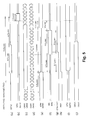
- Fig. 5 shows an example of a timing chart for each of the control signals generated by the T/C 160 shown in Fig. 2 for controlling the display panel, around an H return period.
- the T/C 160 comprises an H counter and counts CKB1 or CKB2 shown in Fig. 5 (d) both of which are produced based on a master clock MCLK (not shown).
- a horizontal synchronization signal of Fig. 5 (a) is detected (in this example, at the L level)
- the H counter is reset.
- a horizontal start pulse STH shown in Fig. 5 (b) (XSTH is the inverted signal of STH) is output to the H driver 220 of the panel 200 based on the count value of the H counter which is updated every 1H.
- Fig. 5 (c) shows a horizontal clock CKH1 (CKH2 is the inverted signal of CKH1) which is output to the H driver 220.
- Fig. 5 (h) shows an inversion control signal FRP for inverting the polarity of the display data signal every 1H. Based on the inversion control signal FRP, the polarity of the display data signal supplied to each data line during one horizontal scan period is controlled.
- Fig. 5 (i) shows a vertical start pulse STV (XSTV is the inverted signal of STV) which is output from the T/C 160 to the V driver 210 once every vertical period based on a vertical synchronization signal Vsync (not shown) .
- the waveform shown in Fig. 5 (j) is a vertical clock CKV1 (CKV2 is the inverted signal of CKV1) which become H level (or L level) once every 1H.
- Fig. 5 (g) shows an opposing voltage inversion control signal COMP-FRP for inverting the polarity of the opposing electrode voltage every 1H, similar to the display data signal.
- the V driver 210 When the vertical start pulse STV is supplied to the V driver 210, the V driver 210 outputs, at every rise (or fall) of the vertical clockCKV1, agate signal (pixel selection signal) to the corresponding gate line 12, so that the pixel TFT 10 connected to the corresponding gate line 12 is controlled to be switched on.
- the switch Hsw is controlled to be switched on and a display data signal is output from a video input line 24 onto the data line 22, which is then applied to the pixel electrode via the pixel TFT 10 in an ON state.
- the potential of the opposing electrode forming the liquid crystal capacity Clc along with the pixel electrode with the liquid crystal in between is controlled to be inverted every 1H.
- the alignment of the liquid crystal between the electrodes is thereby controlled by the potential on the opposing electrode at that time and the potential of the pixel electrode corresponding to the display data signal.
- an enable signal ENB as shown in Fig. 5 (e) (XENB is the inverted signal of ENB) is output to the V driver 210 and H driver 220 based on the count value of the master clock counted by the H counter from the output of the horizontal synchronization signals.
- the V driver 210 stops the output of gate signals to the gate lines 12 during a period when output is forbidden in the V driver 210 as instructed by the enable signal ENB.
- the H driver 220 stops output of data line selection signals to the switches Hsw. Therefore, when the enable signal is being output, no display data signal is output onto the data lines 22 and no gate selection signal is output to the gate lines 12.
- the enable signal ENB is output for a duration of, for example, 7.2 ⁇ sec, and the T/C 160 outputs an alleviation control signal MC as shown in Fig. 5 (f) (XMC is the inverted signal of MC) to the H driver 220 after a predetermined amount of time has elapsed (for example, 2.7 ⁇ sec) since the start of output of the enable signal ENB, based on the counter value by the H counter.
- the control signal MC is output for a duration of, for example, 4.0 usec and is always completed before completion of the output period of the enable signal ENB.
- the H driver switches to an ON state all of the alleviating voltage output switches Msw, each of which is provided between the VM line 26 onto which the change alleviating voltage signal VM is output and each of the data lines 22, as shown in Fig. 1.
- the alleviating voltage output switches Msw are switched on so that the alleviating voltage VM which is equal to the video center voltage Vc (for example, 3.5 V) is applied to each of the data lines 22.
- the polarity of the opposing voltage inversion control signal COM-FRP shown in Fig. 5 (g) is inverted after the output of the enable signal ENB is started and after the alleviation control signal MC is output.
- the switch 140 shown in Fig. 2 is switched, and the opposing electrode voltage is inverted.
- each of the data lines 22 is connected to the VM line 26 via a corresponding switchMsw, as described above. Therefore, even when the opposing electrode voltage is changed, the voltage on the data line 22 is less likely to change, and the reverse bias to the switches Hsw is reduced during the opposing voltage change, as shown in Figs. 4C and 4F.
Landscapes
- Engineering & Computer Science (AREA)
- Chemical & Material Sciences (AREA)
- Crystallography & Structural Chemistry (AREA)
- Physics & Mathematics (AREA)
- Computer Hardware Design (AREA)
- General Physics & Mathematics (AREA)
- Theoretical Computer Science (AREA)
- Liquid Crystal Display Device Control (AREA)
- Liquid Crystal (AREA)
- Control Of Indicators Other Than Cathode Ray Tubes (AREA)
Applications Claiming Priority (2)
| Application Number | Priority Date | Filing Date | Title |
|---|---|---|---|
| JP2001101768 | 2001-03-30 | ||
| JP2001101768A JP2002297110A (ja) | 2001-03-30 | 2001-03-30 | アクティブマトリクス型液晶表示装置の駆動方法 |
Publications (2)
| Publication Number | Publication Date |
|---|---|
| EP1246160A2 true EP1246160A2 (de) | 2002-10-02 |
| EP1246160A3 EP1246160A3 (de) | 2003-01-15 |
Family
ID=18955041
Family Applications (1)
| Application Number | Title | Priority Date | Filing Date |
|---|---|---|---|
| EP02252388A Withdrawn EP1246160A3 (de) | 2001-03-30 | 2002-04-02 | Steuerverfahren für Flüssigkristallanzeige mit aktiver Matrix |
Country Status (6)
| Country | Link |
|---|---|
| US (1) | US7002543B2 (de) |
| EP (1) | EP1246160A3 (de) |
| JP (1) | JP2002297110A (de) |
| KR (1) | KR100464898B1 (de) |
| CN (1) | CN1201187C (de) |
| TW (1) | TW535139B (de) |
Families Citing this family (18)
| Publication number | Priority date | Publication date | Assignee | Title |
|---|---|---|---|---|
| JP2003173174A (ja) | 2001-09-25 | 2003-06-20 | Sharp Corp | 画像表示装置および表示駆動方法 |
| JP4638117B2 (ja) * | 2002-08-22 | 2011-02-23 | シャープ株式会社 | 表示装置およびその駆動方法 |
| JP4120326B2 (ja) * | 2002-09-13 | 2008-07-16 | ソニー株式会社 | 電流出力型駆動回路およびディスプレイデバイス |
| JP4326242B2 (ja) * | 2003-03-13 | 2009-09-02 | 株式会社 日立ディスプレイズ | 液晶表示装置 |
| JP3870933B2 (ja) * | 2003-06-24 | 2007-01-24 | ソニー株式会社 | 表示装置及びその駆動方法 |
| JP2005274658A (ja) * | 2004-03-23 | 2005-10-06 | Hitachi Displays Ltd | 液晶表示装置 |
| JP2005283702A (ja) * | 2004-03-29 | 2005-10-13 | Sony Corp | 表示パネル、表示装置、半導体集積回路及び電子機器 |
| KR101142995B1 (ko) * | 2004-12-13 | 2012-05-08 | 삼성전자주식회사 | 표시 장치 및 그 구동 방법 |
| KR101112555B1 (ko) * | 2005-05-04 | 2012-03-13 | 삼성전자주식회사 | 표시 장치 및 그 구동 방법 |
| KR101136282B1 (ko) * | 2005-06-30 | 2012-04-19 | 엘지디스플레이 주식회사 | 액정표시장치 |
| JP4853028B2 (ja) * | 2006-01-18 | 2012-01-11 | 三菱電機株式会社 | アクティブマトリクス表示装置、およびそのタイミング制御用半導体装置 |
| EP2513966B1 (de) * | 2009-12-18 | 2020-09-16 | Semiconductor Energy Laboratory Co., Ltd. | Halbleiterbauelement |
| WO2011089832A1 (en) * | 2010-01-20 | 2011-07-28 | Semiconductor Energy Laboratory Co., Ltd. | Method for driving display device and liquid crystal display device |
| US9201540B2 (en) * | 2011-09-07 | 2015-12-01 | Apple Inc. | Charge recycling system and method |
| WO2013084813A1 (ja) * | 2011-12-07 | 2013-06-13 | シャープ株式会社 | 表示装置および電子機器 |
| JP2013218341A (ja) * | 2013-05-20 | 2013-10-24 | Necディスプレイソリューションズ株式会社 | 液晶表示装置および液晶パネルの駆動方法 |
| KR102469296B1 (ko) * | 2015-09-22 | 2022-11-23 | 삼성디스플레이 주식회사 | 표시 패널 구동 장치, 이를 이용하는 표시 패널 구동 방법 및 이를 포함하는 표시 장치 |
| CN105931594B (zh) * | 2016-07-08 | 2018-12-14 | 京东方科技集团股份有限公司 | 像素电路、驱动方法、阵列基板、显示面板和显示装置 |
Family Cites Families (17)
| Publication number | Priority date | Publication date | Assignee | Title |
|---|---|---|---|---|
| JPS6066236A (ja) * | 1983-09-21 | 1985-04-16 | Canon Inc | 液晶デイスプレイパネルの駆動法 |
| JPH0685108B2 (ja) * | 1985-08-29 | 1994-10-26 | キヤノン株式会社 | マトリクス表示パネル |
| DE69224959T2 (de) * | 1991-11-07 | 1998-08-13 | Canon Kk | Flüssigkristallvorrichtung und Steuerverfahren dafür |
| JPH0643833A (ja) * | 1992-04-24 | 1994-02-18 | Toshiba Corp | 液晶表示装置およびその駆動方法 |
| US5426447A (en) * | 1992-11-04 | 1995-06-20 | Yuen Foong Yu H.K. Co., Ltd. | Data driving circuit for LCD display |
| JPH06337657A (ja) | 1993-05-31 | 1994-12-06 | Toshiba Corp | 液晶表示装置 |
| JPH07129127A (ja) * | 1993-11-05 | 1995-05-19 | Internatl Business Mach Corp <Ibm> | 液晶表示装置の駆動方法及び装置 |
| JP3482683B2 (ja) | 1994-04-22 | 2003-12-22 | ソニー株式会社 | アクティブマトリクス表示装置及びその駆動方法 |
| TW275684B (de) * | 1994-07-08 | 1996-05-11 | Hitachi Seisakusyo Kk | |
| JP3501530B2 (ja) * | 1994-12-22 | 2004-03-02 | キヤノン株式会社 | アクティブマトリックス液晶表示装置とその駆動方法 |
| JP3424387B2 (ja) | 1995-04-11 | 2003-07-07 | ソニー株式会社 | アクティブマトリクス表示装置 |
| US6229515B1 (en) * | 1995-06-15 | 2001-05-08 | Kabushiki Kaisha Toshiba | Liquid crystal display device and driving method therefor |
| JP3131411B2 (ja) | 1997-12-01 | 2001-01-31 | ソニー株式会社 | 液晶ディスプレイ装置 |
| JPH11327518A (ja) * | 1998-03-19 | 1999-11-26 | Sony Corp | 液晶表示装置 |
| JP4081852B2 (ja) * | 1998-04-30 | 2008-04-30 | ソニー株式会社 | 有機el素子のマトリクス駆動方法及び有機el素子のマトリクス駆動装置 |
| US6486864B1 (en) * | 1999-03-10 | 2002-11-26 | Sharp Kabushiki Kaisha | Liquid crystal display device, and method for driving the same |
| JP2001272654A (ja) | 2000-03-28 | 2001-10-05 | Sanyo Electric Co Ltd | アクティブマトリクス型液晶表示装置 |
-
2001
- 2001-03-30 JP JP2001101768A patent/JP2002297110A/ja active Pending
-
2002
- 2002-02-07 TW TW091102166A patent/TW535139B/zh not_active IP Right Cessation
- 2002-03-28 US US10/113,097 patent/US7002543B2/en not_active Expired - Lifetime
- 2002-03-29 CN CNB021049874A patent/CN1201187C/zh not_active Expired - Fee Related
- 2002-03-29 KR KR10-2002-0017339A patent/KR100464898B1/ko not_active Expired - Lifetime
- 2002-04-02 EP EP02252388A patent/EP1246160A3/de not_active Withdrawn
Non-Patent Citations (1)
| Title |
|---|
| None * |
Also Published As
| Publication number | Publication date |
|---|---|
| KR100464898B1 (ko) | 2005-01-06 |
| EP1246160A3 (de) | 2003-01-15 |
| TW535139B (en) | 2003-06-01 |
| CN1379378A (zh) | 2002-11-13 |
| US7002543B2 (en) | 2006-02-21 |
| US20020140661A1 (en) | 2002-10-03 |
| CN1201187C (zh) | 2005-05-11 |
| KR20020077246A (ko) | 2002-10-11 |
| JP2002297110A (ja) | 2002-10-11 |
Similar Documents
| Publication | Publication Date | Title |
|---|---|---|
| US5959600A (en) | Active matrix display device | |
| US7808472B2 (en) | Liquid crystal display and driving method thereof | |
| US7002543B2 (en) | Method for driving active matrix type liquid crystal display | |
| US8217929B2 (en) | Electro-optical device, driving method, and electronic apparatus with user adjustable ratio between positive and negative field | |
| US7777737B2 (en) | Active matrix type liquid crystal display device | |
| KR100389027B1 (ko) | 액정표시장치 및 그 구동방법 | |
| US20020196247A1 (en) | Display device | |
| CN1996105B (zh) | 液晶显示装置 | |
| US8009155B2 (en) | Output buffer of a source driver applied in a display | |
| JP2007279539A (ja) | ドライバ回路、表示装置及びその駆動方法 | |
| US20100118016A1 (en) | Video voltage supplying circuit, electro-optical apparatus and electronic apparatus | |
| JPH11161237A (ja) | 液晶表示装置 | |
| JP5418388B2 (ja) | 液晶表示装置 | |
| JP3443059B2 (ja) | 残像消去方法および該残像消去方法を用いた表示装置 | |
| JP4612349B2 (ja) | 液晶表示装置 | |
| KR100667184B1 (ko) | 액정표시장치의 소스 구동장치 | |
| JP2006106019A (ja) | 液晶表示装置及び液晶表示装置の駆動制御方法 | |
| KR101352936B1 (ko) | 액정 표시 장치 | |
| JPS63172193A (ja) | アクテイブマトリクス型表示装置の駆動方法 | |
| KR101197757B1 (ko) | 액정 표시 장치의 데이터 처리 방법 및 장치 | |
| KR101194647B1 (ko) | 액정표시장치의 공통전극 구동회로 | |
| JP3366354B2 (ja) | Tftアクティブマトリクス液晶表示装置及びその駆動方法 | |
| KR20070070766A (ko) | 액정표시장치 | |
| JP2006126346A (ja) | 液晶表示装置及びその駆動方法 | |
| KR20060078674A (ko) | 액정표시장치 및 이의 구동방법 |
Legal Events
| Date | Code | Title | Description |
|---|---|---|---|
| PUAI | Public reference made under article 153(3) epc to a published international application that has entered the european phase |
Free format text: ORIGINAL CODE: 0009012 |
|
| AK | Designated contracting states |
Kind code of ref document: A2 Designated state(s): AT BE CH CY DE DK ES FI FR GB GR IE IT LI LU MC NL PT SE TR |
|
| AX | Request for extension of the european patent |
Free format text: AL;LT;LV;MK;RO;SI |
|
| PUAL | Search report despatched |
Free format text: ORIGINAL CODE: 0009013 |
|
| AK | Designated contracting states |
Kind code of ref document: A3 Designated state(s): AT BE CH CY DE DK ES FI FR GB GR IE IT LI LU MC NL PT SE TR |
|
| AX | Request for extension of the european patent |
Free format text: AL;LT;LV;MK;RO;SI |
|
| 17P | Request for examination filed |
Effective date: 20030619 |
|
| 17Q | First examination report despatched |
Effective date: 20030805 |
|
| AKX | Designation fees paid |
Designated state(s): DE FI FR GB NL |
|
| 17Q | First examination report despatched |
Effective date: 20030805 |
|
| STAA | Information on the status of an ep patent application or granted ep patent |
Free format text: STATUS: THE APPLICATION IS DEEMED TO BE WITHDRAWN |
|
| 18D | Application deemed to be withdrawn |
Effective date: 20070417 |