EP1246237A2 - Verfahren zur Herstellung von Isolationsgräben zwischen aktiven Bereichen einer E2PROM-Zelle - Google Patents
Verfahren zur Herstellung von Isolationsgräben zwischen aktiven Bereichen einer E2PROM-Zelle Download PDFInfo
- Publication number
- EP1246237A2 EP1246237A2 EP01307982A EP01307982A EP1246237A2 EP 1246237 A2 EP1246237 A2 EP 1246237A2 EP 01307982 A EP01307982 A EP 01307982A EP 01307982 A EP01307982 A EP 01307982A EP 1246237 A2 EP1246237 A2 EP 1246237A2
- Authority
- EP
- European Patent Office
- Prior art keywords
- layer
- trenches
- substrate
- insulating material
- conductive
- Prior art date
- Legal status (The legal status is an assumption and is not a legal conclusion. Google has not performed a legal analysis and makes no representation as to the accuracy of the status listed.)
- Withdrawn
Links
Images

Classifications
-
- H—ELECTRICITY
- H10—SEMICONDUCTOR DEVICES; ELECTRIC SOLID-STATE DEVICES NOT OTHERWISE PROVIDED FOR
- H10B—ELECTRONIC MEMORY DEVICES
- H10B41/00—Electrically erasable-and-programmable ROM [EEPROM] devices comprising floating gates
- H10B41/30—Electrically erasable-and-programmable ROM [EEPROM] devices comprising floating gates characterised by the memory core region
-
- H—ELECTRICITY
- H10—SEMICONDUCTOR DEVICES; ELECTRIC SOLID-STATE DEVICES NOT OTHERWISE PROVIDED FOR
- H10W—GENERIC PACKAGES, INTERCONNECTIONS, CONNECTORS OR OTHER CONSTRUCTIONAL DETAILS OF DEVICES COVERED BY CLASS H10
- H10W10/00—Isolation regions in semiconductor bodies between components of integrated devices
-
- H—ELECTRICITY
- H10—SEMICONDUCTOR DEVICES; ELECTRIC SOLID-STATE DEVICES NOT OTHERWISE PROVIDED FOR
- H10B—ELECTRONIC MEMORY DEVICES
- H10B69/00—Erasable-and-programmable ROM [EPROM] devices not provided for in groups H10B41/00 - H10B63/00, e.g. ultraviolet erasable-and-programmable ROM [UVEPROM] devices
-
- H—ELECTRICITY
- H10—SEMICONDUCTOR DEVICES; ELECTRIC SOLID-STATE DEVICES NOT OTHERWISE PROVIDED FOR
- H10W—GENERIC PACKAGES, INTERCONNECTIONS, CONNECTORS OR OTHER CONSTRUCTIONAL DETAILS OF DEVICES COVERED BY CLASS H10
- H10W10/00—Isolation regions in semiconductor bodies between components of integrated devices
- H10W10/01—Manufacture or treatment
-
- H—ELECTRICITY
- H10—SEMICONDUCTOR DEVICES; ELECTRIC SOLID-STATE DEVICES NOT OTHERWISE PROVIDED FOR
- H10W—GENERIC PACKAGES, INTERCONNECTIONS, CONNECTORS OR OTHER CONSTRUCTIONAL DETAILS OF DEVICES COVERED BY CLASS H10
- H10W10/00—Isolation regions in semiconductor bodies between components of integrated devices
- H10W10/01—Manufacture or treatment
- H10W10/011—Manufacture or treatment of isolation regions comprising dielectric materials
- H10W10/014—Manufacture or treatment of isolation regions comprising dielectric materials using trench refilling with dielectric materials, e.g. shallow trench isolations
-
- H—ELECTRICITY
- H10—SEMICONDUCTOR DEVICES; ELECTRIC SOLID-STATE DEVICES NOT OTHERWISE PROVIDED FOR
- H10W—GENERIC PACKAGES, INTERCONNECTIONS, CONNECTORS OR OTHER CONSTRUCTIONAL DETAILS OF DEVICES COVERED BY CLASS H10
- H10W10/00—Isolation regions in semiconductor bodies between components of integrated devices
- H10W10/10—Isolation regions comprising dielectric materials
- H10W10/17—Isolation regions comprising dielectric materials formed using trench refilling with dielectric materials, e.g. shallow trench isolations
Definitions
- the present invention relates to a self-aligned method of forming a semiconductor memory array of floating gate memory cells, and more particularly to an improved method of forming the isolation regions between active regions in which the memory cells are formed.
- Non-volatile semiconductor memory cells using a floating gate to store charges thereon and memory arrays of such non-volatile memory cells formed in a semiconductor substrate are well known in the art.
- floating gate memory cells have been of the split gate type, or stacked gate type, or a combination thereof.
- Self-alignment is well known in the art. Self-alignment refers to the act of processing one or more steps involving one or more materials such that the features are automatically aligned with respect to one another in that step processing. Accordingly, the present invention uses the technique of self-alignment to achieve the manufacturing of the isolation regions used in a semiconductor memory array, such as one with a floating gate memory cell type.
- FIG. 1A-1B show the well known shallow trench process (STI) for forming isolation regions between active regions of a memory array semiconductor device.
- a first layer of insulation material 12 such as silicon dioxide (“oxide")
- a layer of polysilicon 14 (used to form the floating gate) is deposited on top of the layer of insulation material 12.
- a silicon nitride layer 16 (“nitride") is deposited over the polysilicon layer 14.
- a suitable photo-resistant material 18 is then applied on the silicon nitride layer 16 and a masking step is performed to selectively remove the photo-resistant material from certain regions (stripes 20).
- the silicon nitride 16, the polysilicon 14 and the underlying insulation material 12 are etched away in parallel stripes 20 using standard etching techniques (i.e. anisotropic etch process). The etching continues to form trenches 22 that extend down into the substrate 10. As the silicon substrate is etched to form trench 22, a slight lateral undercut 26 is formed, where the oxide layer 12 and poly layer 14 overhang the trench 22. Where the photo resist 18 is not removed, the silicon nitride 16, the first polysilicon region 14 and the underlying insulation region 12 are maintained.
- the structure is further processed to remove the remaining photo resist 18, which is followed by the formation of an isolation material 24, such as silicon dioxide, in the trenches 22 (e.g. by depositing an oxide layer, followed by a CMP etch). Then, the nitride layer 16 is selectively removed. The resulting structure is shown in Fig. 1B.
- the remaining polysilicon layer 14 and the underlying first insulation material 12 form the active regions in which the memory cells are formed.
- the substrate 10 has alternating stripes of active regions and isolation regions with the isolation regions being formed of the shallow trench insulation material 24.
- Fig. 1B represents a self aligned structure, which is more compact than a structure formed by a non self-aligned method.
- problems can occur with this structure after the isolation is completed and during the formation of the memory cells.
- Fig. 1C illustrates the structure after back processing steps are performed to complete the formation of the memory cell array structure.
- Poly layer loss is typical in such back processing steps, whereby the side edges of poly layer 14 that at one time extended over to overhang the isolation trench 22 are later are pulled back away from the isolation trench 22. This results in a gap ⁇ between the side edges of the poly layer 14 and the edges of the isolation trench 22, leaving a portion of oxide layer 12 and the substrate 10 exposed and unprotected by the poly layer 14.
- this structure is prone to silicon pitting in the active region, where processing steps which rely on the protection by poly layer 14 tend to damage oxide layer 12 and substrate 10 in the gap region ⁇ . Further, the electrical performance of the final product is adversely affected because the poly layer 14 (which forms the floating gate that controls conduction in the underlying substrate) no longer overlays the full width of the substrate 10 between adjacent isolation trenches.
- One further disadvantage of conventional STI isolation is that poly layer lifting occurs (i.e. smiling effect), which means the thickness of the oxide layer 12 near the side edges of the poly layer 14 increases. Poly layer lifting occurs because the poly layer 14 is formed before isolation trench oxide 24 is formed.
- the present invention solves the aforementioned problems by utilizing a process that self aligns the poly layer to the diffusion edge, where an increased overlap is formed between the side edges of the poly layer and the isolation regions.
- the process of the present invention can be independently optimized in a self-aligned manner.
- the present invention is a self-aligned method of forming isolation and active regions in a semiconductor device, and includes the steps of forming a layer of first material on a semiconductor substrate, forming a plurality of spaced apart trenches that extend through the layer of first material and into the substrate, forming a first layer of insulating material along sidewall portions of the trenches, filling the trenches with an insulating material, removing the layer of first material to expose portions of the substrate, forming a second layer of insulating material on the exposed portions of the substrate, and forming a layer of conductive material on the second layer of insulating material.
- a semiconductor structure for use in the manufacture of an electrically programmable and erasable memory device includes a substrate of semiconductor material of a first conductivity type, a first layer of insulating material formed on the substrate, a layer of conductive material formed on the first layer of insulating material, a plurality of spaced apart trenches formed through the first layer of insulating material and the layer of conductive material and into the substrate, a second layer of insulation material formed on sidewall portions of the trenches, and a block of insulation material formed in the trenches. For each of the trenches, an edge portion of the layer of conductive material extends over and overlaps with the first layer of insulating material by a predetermined distance ⁇ .
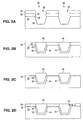
- a semiconductor substrate 30 which is preferably of P type and is well known in the art.
- a silicon nitride layer 32 (hereinafter “nitride”) is deposited over the silicon substrate 30, preferably by chemical vapor deposition (CVD).
- a suitable photo-resistant material 34 is applied on the nitride layer 32, and a masking step is performed to selectively remove the photo-resistant material from parallel stripe regions 36. Where the photo-resist material 34 is removed, the exposed stripes of nitride layer 32 are etched away using standard etching techniques (i.e. anisotropic etch process) to expose stripes of the underlying silicon substrate 30.
- a silicon etch process is then performed in the stripes 36 to form trenches 38 that extend through nitride layer 32 and into the silicon substrate 30.
- the trenches are originally defined by nitride edge 42 and sidewall portions 39 formed in the silicon substrate 30.
- the resulting structure is illustrated in Fig. 2A, and includes slight undercut portions 40 where the edges 42 of the nitride layer extend beyond trench sidewall portions 39 formed in the silicon substrate 30.
- the structure is further processed to remove the remaining photo resist 34.
- a linear oxidation process is performed to form oxide layers 44 along trench sidewall portions 39 in the substrate 30 by passivating the trench sidewall portions 39.
- This oxidation step further pushes the trench sidewall portions 39 laterally underneath the nitride layer 32, which increases the width of trenches 38 in substrate 10 and enhances the undercut portions 40 by creating a self aligned offset between the sidewall portions 39 and the adjacent edge 42 of the nitride layer 32.
- the trenches 38 are then filled with oxide to form oxide blocks 46 by conventional oxide deposition and planarization (e.g. CMP).
- CMP oxide deposition and planarization
- nitride etch (wet or dry) process is performed to remove nitride layer 32.
- An insulating layer 48 is then formed on the exposed portions of the substrate 10.
- insulating layer 48 is an oxide layer formed by oxide deposition (e.g. CVD) or by oxidizing the exposed surface of the substrate 30. The resulting structure is shown in Fig. 2C.
- a conductive layer 50 is then formed over the insulating (oxide) layer 48 so that its top surface is even with the top surface of trench oxide 46.
- the conductive layer is formed by a polysilicon deposition process, followed by CMP planarization. The resulting structure is shown in Fig. 2D.
- the isolation regions are now defined by the combination of the oxide blocks 46 and the oxide layers 44.
- the size of this overlap distance ⁇ is dictated primarily by the thickness of the oxide layer 44 formed in the isolation trenches 38, which is controllable.
- the overlap distance ⁇ can be independently optimized in a self-aligned manner to provide an enhanced overlap that counteracts the poly layer loss during later back end processing, so that the edges of poly layer 50 are better aligned to the edges of the isolation regions once all processing steps are completed. Further, since the poly layer 50 is formed after the formation of trench oxide 46, insulating oxide 48 and oxide layers 44, poly lifting is avoided.
- the present invention is not limited to the embodiment described above and illustrated herein, but encompasses any and all variations falling within the scope of the appended claims.
- the foregoing method describes the use of polysilicon as the conductive material, and nitride and oxide as insulation materials, it should be clear to those having ordinary skill in the art that any appropriate conductive material and insulation materials can be used.
- the thickness of oxide layer 44 can be less than the length of overhang portion 40, whereby the edge 52 of conductive layer 50 will also partially extend over and overlap with a portion of corresponding oxide block 46.
Landscapes
- Non-Volatile Memory (AREA)
- Semiconductor Memories (AREA)
- Element Separation (AREA)
Applications Claiming Priority (4)
| Application Number | Priority Date | Filing Date | Title |
|---|---|---|---|
| US28031301P | 2001-03-29 | 2001-03-29 | |
| US280313P | 2001-03-29 | ||
| US09/916,423 US6627942B2 (en) | 2001-03-29 | 2001-07-26 | Self-aligned floating gate poly for a flash E2PROM cell |
| US916423 | 2001-07-26 |
Publications (1)
| Publication Number | Publication Date |
|---|---|
| EP1246237A2 true EP1246237A2 (de) | 2002-10-02 |
Family
ID=26960198
Family Applications (1)
| Application Number | Title | Priority Date | Filing Date |
|---|---|---|---|
| EP01307982A Withdrawn EP1246237A2 (de) | 2001-03-29 | 2001-09-19 | Verfahren zur Herstellung von Isolationsgräben zwischen aktiven Bereichen einer E2PROM-Zelle |
Country Status (6)
| Country | Link |
|---|---|
| US (1) | US6627942B2 (de) |
| EP (1) | EP1246237A2 (de) |
| JP (1) | JP2002299479A (de) |
| KR (1) | KR100811576B1 (de) |
| CN (1) | CN1290171C (de) |
| TW (1) | TW523880B (de) |
Families Citing this family (6)
| Publication number | Priority date | Publication date | Assignee | Title |
|---|---|---|---|---|
| KR100541554B1 (ko) * | 2003-12-09 | 2006-01-12 | 삼성전자주식회사 | 플래쉬 메모리 소자의 제조방법 및 그에 의해 제조된플래쉬 메모리 소자 |
| US7183161B2 (en) * | 2004-09-17 | 2007-02-27 | Freescale Semiconductor, Inc. | Programming and erasing structure for a floating gate memory cell and method of making |
| US7094645B2 (en) * | 2004-09-17 | 2006-08-22 | Freescale Semiconductor, Inc. | Programming and erasing structure for a floating gate memory cell and method of making |
| US7307002B2 (en) * | 2005-04-04 | 2007-12-11 | Spansion Llc | Non-critical complementary masking method for poly-1 definition in flash memory device fabrication |
| KR100723767B1 (ko) * | 2005-11-10 | 2007-05-30 | 주식회사 하이닉스반도체 | 플래쉬 메모리 소자 및 그 제조방법 |
| US9368579B2 (en) * | 2012-02-07 | 2016-06-14 | The Board Of Trustees Of The Leland Stanford Junior University | Selective area growth of germanium and silicon-germanium in silicon waveguides for on-chip optical interconnect applications |
Family Cites Families (30)
| Publication number | Priority date | Publication date | Assignee | Title |
|---|---|---|---|---|
| US5808328A (en) | 1977-02-21 | 1998-09-15 | Zaidan Hojin Handotai Kenkyu Shinkokai | High-speed and high-density semiconductor memory |
| US4757360A (en) | 1983-07-06 | 1988-07-12 | Rca Corporation | Floating gate memory device with facing asperities on floating and control gates |
| US4947221A (en) | 1985-11-29 | 1990-08-07 | General Electric Company | Memory cell for a dense EPROM |
| IT1191566B (it) | 1986-06-27 | 1988-03-23 | Sgs Microelettronica Spa | Dispositivo di memoria non labile a semiconduttore del tipo a porta non connessa (floating gate) alterabile elettricamente con area di tunnel ridotta e procedimento di fabbricazione |
| US4794565A (en) | 1986-09-15 | 1988-12-27 | The Regents Of The University Of California | Electrically programmable memory device employing source side injection |
| KR910000139B1 (ko) | 1986-10-27 | 1991-01-21 | 가부시키가이샤 도시바 | 불휘발성 반도체기억장치 |
| US5268319A (en) | 1988-06-08 | 1993-12-07 | Eliyahou Harari | Highly compact EPROM and flash EEPROM devices |
| JP2600301B2 (ja) | 1988-06-28 | 1997-04-16 | 三菱電機株式会社 | 半導体記憶装置およびその製造方法 |
| US5051793A (en) | 1989-03-27 | 1991-09-24 | Ict International Cmos Technology, Inc. | Coplanar flash EPROM cell and method of making same |
| KR940006094B1 (ko) | 1989-08-17 | 1994-07-06 | 삼성전자 주식회사 | 불휘발성 반도체 기억장치 및 그 제조방법 |
| US5572054A (en) | 1990-01-22 | 1996-11-05 | Silicon Storage Technology, Inc. | Method of operating a single transistor non-volatile electrically alterable semiconductor memory device |
| US5029130A (en) | 1990-01-22 | 1991-07-02 | Silicon Storage Technology, Inc. | Single transistor non-valatile electrically alterable semiconductor memory device |
| US5021848A (en) | 1990-03-13 | 1991-06-04 | Chiu Te Long | Electrically-erasable and electrically-programmable memory storage devices with self aligned tunnel dielectric area and the method of fabricating thereof |
| JP2815495B2 (ja) | 1991-07-08 | 1998-10-27 | ローム株式会社 | 半導体記憶装置 |
| US5544103A (en) | 1992-03-03 | 1996-08-06 | Xicor, Inc. | Compact page-erasable eeprom non-volatile memory |
| JP3133667B2 (ja) | 1995-02-23 | 2001-02-13 | 三洋電機株式会社 | スプリットゲート型トランジスタ、スプリットゲート型トランジスタの製造方法、不揮発性半導体メモリ |
| US5780892A (en) | 1995-03-21 | 1998-07-14 | Winbond Electronics Corporation | Flash E2 PROM cell structure with poly floating and control gates |
| KR0144906B1 (ko) | 1995-03-31 | 1998-07-01 | 김광호 | 불휘발성 메모리 소자 및 그 제조방법 |
| US5597751A (en) | 1995-12-20 | 1997-01-28 | Winbond Electronics Corp. | Single-side oxide sealed salicide process for EPROMs |
| US5814853A (en) | 1996-01-22 | 1998-09-29 | Advanced Micro Devices, Inc. | Sourceless floating gate memory device and method of storing data |
| US5780341A (en) | 1996-12-06 | 1998-07-14 | Halo Lsi Design & Device Technology, Inc. | Low voltage EEPROM/NVRAM transistors and making method |
| US6165853A (en) * | 1997-06-16 | 2000-12-26 | Micron Technology, Inc. | Trench isolation method |
| US6306725B1 (en) * | 1997-11-19 | 2001-10-23 | Texas Instruments Incorporated | In-situ liner for isolation trench side walls and method |
| US6008108A (en) * | 1998-12-07 | 1999-12-28 | United Microelectronics Corp. | Method of fabricating a shallow-trench isolation structure in an integrated circuit |
| US6180467B1 (en) * | 1998-12-15 | 2001-01-30 | United Microelectronics Corp. | Method of fabricating shallow trench isolation |
| US6091104A (en) | 1999-03-24 | 2000-07-18 | Chen; Chiou-Feng | Flash memory cell with self-aligned gates and fabrication process |
| US6140182A (en) | 1999-02-23 | 2000-10-31 | Actrans System Inc. | Nonvolatile memory with self-aligned floating gate and fabrication process |
| KR100281192B1 (ko) * | 1999-03-04 | 2001-01-15 | 황인길 | 반도체 소자 분리를 위한 얕은 트렌치 제조 방법 |
| US6103573A (en) | 1999-06-30 | 2000-08-15 | Sandisk Corporation | Processing techniques for making a dual floating gate EEPROM cell array |
| US6222227B1 (en) | 1999-08-09 | 2001-04-24 | Actrans System Inc. | Memory cell with self-aligned floating gate and separate select gate, and fabrication process |
-
2001
- 2001-07-26 US US09/916,423 patent/US6627942B2/en not_active Expired - Lifetime
- 2001-09-19 EP EP01307982A patent/EP1246237A2/de not_active Withdrawn
- 2001-09-19 JP JP2001284379A patent/JP2002299479A/ja not_active Withdrawn
- 2001-09-19 KR KR1020010057992A patent/KR100811576B1/ko not_active Expired - Fee Related
- 2001-09-19 CN CNB011379057A patent/CN1290171C/zh not_active Expired - Fee Related
- 2001-09-19 TW TW090123069A patent/TW523880B/zh not_active IP Right Cessation
Also Published As
| Publication number | Publication date |
|---|---|
| KR20020077013A (ko) | 2002-10-11 |
| KR100811576B1 (ko) | 2008-03-10 |
| CN1378263A (zh) | 2002-11-06 |
| US6627942B2 (en) | 2003-09-30 |
| CN1290171C (zh) | 2006-12-13 |
| US20020142544A1 (en) | 2002-10-03 |
| TW523880B (en) | 2003-03-11 |
| JP2002299479A (ja) | 2002-10-11 |
Similar Documents
| Publication | Publication Date | Title |
|---|---|---|
| CN111418063A (zh) | 具有集成高k金属控制栅的非易失性分裂栅存储器单元及制造方法 | |
| JP2001102467A (ja) | フローティングゲートメモリセルの半導体メモリアレイ、このアレイを形成する自己整合方法、不揮発性メモリセルのアレイを有する半導体装置、及び、複数の半導体素子に接続する複数の行ラインと列ラインを形成する方法 | |
| US20150014761A1 (en) | Semiconductor device and manufacturing method thereof | |
| US8378395B2 (en) | Methods of fabricating field effect transistors having protruded active regions | |
| US6218265B1 (en) | Process for fabricating a semiconductor non-volatile memory device with shallow trench isolation (STI) | |
| US6858494B2 (en) | Structure and fabricating method with self-aligned bit line contact to word line in split gate flash | |
| US20050282337A1 (en) | High write and erase efficiency embedded flash cell | |
| US6627942B2 (en) | Self-aligned floating gate poly for a flash E2PROM cell | |
| US6953973B2 (en) | Self-aligned trench isolation method and semiconductor device fabricated using the same | |
| US6800525B2 (en) | Method of manufacturing split gate flash memory device | |
| KR20010003086A (ko) | 플로팅 게이트 형성 방법 | |
| EP2904631B1 (de) | Selbstjustierendes verfahren zur herstellung einer halbleiterspeichermatrix aus floating-gate-speicherzellen mit einer einzelpolyschicht | |
| JP4537618B2 (ja) | 半導体装置及びその製造方法 | |
| EP1782460B1 (de) | Herstellungsverfahren für eine Floating-Gate-Speicherzelle | |
| US8963220B2 (en) | Shallow trench isolation for a memory | |
| KR100330948B1 (ko) | 비휘발성 반도체 메모리 장치 및 그 제조방법 | |
| US20050064662A1 (en) | [method of fabricating flash memory] | |
| KR100641507B1 (ko) | 플래시 메모리의 부유 게이트 형성 방법 | |
| US7855124B2 (en) | Method for forming a semiconductor device | |
| CN118102728A (zh) | 非易失性存储器结构及其形成方法 | |
| KR20070032833A (ko) | 불휘발성 메모리 장치의 제조방법 | |
| KR20060133253A (ko) | 불휘발성 메모리 장치의 제조 방법 |
Legal Events
| Date | Code | Title | Description |
|---|---|---|---|
| PUAI | Public reference made under article 153(3) epc to a published international application that has entered the european phase |
Free format text: ORIGINAL CODE: 0009012 |
|
| AK | Designated contracting states |
Kind code of ref document: A2 Designated state(s): AT BE CH CY DE DK ES FI FR GB GR IE IT LI LU MC NL PT SE TR |
|
| AX | Request for extension of the european patent |
Free format text: AL;LT;LV;MK;RO;SI |
|
| STAA | Information on the status of an ep patent application or granted ep patent |
Free format text: STATUS: THE APPLICATION HAS BEEN WITHDRAWN |
|
| 18W | Application withdrawn |
Effective date: 20030731 |