EP1246246A2 - Lichtemittierende Vorrichtung und Herstellungsverfahren - Google Patents
Lichtemittierende Vorrichtung und Herstellungsverfahren Download PDFInfo
- Publication number
- EP1246246A2 EP1246246A2 EP02252386A EP02252386A EP1246246A2 EP 1246246 A2 EP1246246 A2 EP 1246246A2 EP 02252386 A EP02252386 A EP 02252386A EP 02252386 A EP02252386 A EP 02252386A EP 1246246 A2 EP1246246 A2 EP 1246246A2
- Authority
- EP
- European Patent Office
- Prior art keywords
- pixels
- pixel
- emissive layer
- organic
- electrode
- Prior art date
- Legal status (The legal status is an assumption and is not a legal conclusion. Google has not performed a legal analysis and makes no representation as to the accuracy of the status listed.)
- Withdrawn
Links
- 238000004519 manufacturing process Methods 0.000 title claims description 6
- 230000005525 hole transport Effects 0.000 claims abstract description 15
- 239000011159 matrix material Substances 0.000 claims abstract description 11
- 238000000034 method Methods 0.000 claims description 9
- 239000000463 material Substances 0.000 claims description 7
- 238000005401 electroluminescence Methods 0.000 claims description 3
- 239000010409 thin film Substances 0.000 abstract description 23
- 239000010408 film Substances 0.000 abstract description 16
- 238000007740 vapor deposition Methods 0.000 abstract description 2
- 239000010410 layer Substances 0.000 description 83
- 239000003990 capacitor Substances 0.000 description 9
- 238000003860 storage Methods 0.000 description 9
- 239000000758 substrate Substances 0.000 description 9
- 239000004065 semiconductor Substances 0.000 description 5
- 230000000694 effects Effects 0.000 description 4
- 238000001704 evaporation Methods 0.000 description 4
- 230000008020 evaporation Effects 0.000 description 4
- 238000012986 modification Methods 0.000 description 3
- 230000004048 modification Effects 0.000 description 3
- 239000012044 organic layer Substances 0.000 description 3
- 230000015572 biosynthetic process Effects 0.000 description 2
- 239000011229 interlayer Substances 0.000 description 2
- NRCMAYZCPIVABH-UHFFFAOYSA-N Quinacridone Chemical class N1C2=CC=CC=C2C(=O)C2=C1C=C1C(=O)C3=CC=CC=C3NC1=C2 NRCMAYZCPIVABH-UHFFFAOYSA-N 0.000 description 1
- GQVWHWAWLPCBHB-UHFFFAOYSA-L beryllium;benzo[h]quinolin-10-olate Chemical compound [Be+2].C1=CC=NC2=C3C([O-])=CC=CC3=CC=C21.C1=CC=NC2=C3C([O-])=CC=CC3=CC=C21 GQVWHWAWLPCBHB-UHFFFAOYSA-L 0.000 description 1
- 238000000151 deposition Methods 0.000 description 1
- 238000009826 distribution Methods 0.000 description 1
- 238000010030 laminating Methods 0.000 description 1
- 238000004020 luminiscence type Methods 0.000 description 1
- 239000002184 metal Substances 0.000 description 1
- 230000001590 oxidative effect Effects 0.000 description 1
- 229910021420 polycrystalline silicon Inorganic materials 0.000 description 1
- 238000007738 vacuum evaporation Methods 0.000 description 1
Images



Classifications
-
- H—ELECTRICITY
- H10—SEMICONDUCTOR DEVICES; ELECTRIC SOLID-STATE DEVICES NOT OTHERWISE PROVIDED FOR
- H10K—ORGANIC ELECTRIC SOLID-STATE DEVICES
- H10K59/00—Integrated devices, or assemblies of multiple devices, comprising at least one organic light-emitting element covered by group H10K50/00
- H10K59/10—OLED displays
- H10K59/12—Active-matrix OLED [AMOLED] displays
-
- H—ELECTRICITY
- H05—ELECTRIC TECHNIQUES NOT OTHERWISE PROVIDED FOR
- H05B—ELECTRIC HEATING; ELECTRIC LIGHT SOURCES NOT OTHERWISE PROVIDED FOR; CIRCUIT ARRANGEMENTS FOR ELECTRIC LIGHT SOURCES, IN GENERAL
- H05B33/00—Electroluminescent light sources
- H05B33/10—Apparatus or processes specially adapted to the manufacture of electroluminescent light sources
-
- H—ELECTRICITY
- H10—SEMICONDUCTOR DEVICES; ELECTRIC SOLID-STATE DEVICES NOT OTHERWISE PROVIDED FOR
- H10K—ORGANIC ELECTRIC SOLID-STATE DEVICES
- H10K71/00—Manufacture or treatment specially adapted for the organic devices covered by this subclass
Definitions
- the present invention relates to a light-emitting device, and more particularly to increasing the effective light emission area.
- Organic EL elements are self emitting displays in which an electrical current is supplied to an organic EL layer, provided between an anode and a cathode, causing the organic EL layer to emit light. Also since a backlight is unnecessary, unlike LCDs, organic EL elements are expected to be the next major type of flat display panel. In particular, in the active matrix type of organic EL display in which a switching element is formed at each pixel, a larger and higher resolution screen is possible since display data can be stored at each respective pixel.
- the organic EL layer which is an emissive layer, is usually formed by a vacuum evapovation process using a shadow mask on a circuit substrate.
- Fig. 6 shows a typical pixel arrangement of a color organic EL display 1.
- the organic EL display 1 comprises a plurality of pixels 1a arranged in a matrix configuration.
- Each pixel 1a has a switching element, such as a thin-film transistor, and the switching element of each pixel is driven by a gate line corresponding to the row and a data line corresponding to a column so as to cause the organic EL element to emit light.
- the arrangement of the R pixels, the G pixels, and the B pixels is arbitrary, the R pixels, the G pixels, and the B pixels may be positioned linearly (stripe arrangement in columns) as shown in the figure, for example.
- Fig. 7 is a detailed top view of the pixel 1a of Fig. 6.
- Fig. 8A and 8B respectively show the cross-sectional views of A-A and B-B of Fig. 7.
- the area enclosed by a gate line 51 extending in the row direction and a data line 52 extending in the column direction represents one pixel area la.
- an n-channel thin-film transistor 13 Within this area are formed an n-channel thin-film transistor 13, a storage capacitor 70, and a p-channel thin-film transistor 42.
- An organic EL element 65 which is connected via a drain electrode 43d to the thin-film transistor 42, is further provided.
- a source of the thin-film transistor 42 is connected to a power line 53 via a source electrode 43s.
- An active layer 9 of the thin-film transistor 13 forms a pattern of a double-gate structure that passes twice underneath gate electrodes 11 protruding from the gate line 51.
- a drain of the thin-film transistor 13 is connected to the data line 52 via a drain electrode 16 and a source is connected to a gate 41 of the thin-film transistor 42 via the storage capacitor 70 and a bridge structure.
- the storage capacitor 70 is formed from an electrode 55 integrated with the active layer 9 and an SC line 54 connected to power Vsc.
- the drain of the thin-film transistor 42 is connected to an organic EL element 60.
- the organic EL element 60 is comprised from an anode (transparent electrode) 61 that is formed at each pixel on a planarization insulating film 17 on the thin-film transistors 13, 42, a cathode (metal electrode) 66 that is formed in common with the pixels on the topmost layer, and an organic layer 65 that is laminated between the anode 61 and the cathode 66.
- the anode 61 is comprised from a material such as ITO and is connected via the drain electrode 43d to the thin-film transistor 42.
- the organic layer 65 is comprised by sequentially laminating from the anode 61, a hole transport layer 62, an organic emissive layer 63, and an electron transport layer 64.
- the organic emissive layer 63 is composed of a different material for the R pixels, the G pixels, and the B pixels, a material containing BeBq 2 that includes a Quinacridon derivative is used.
- each pixel is all laminated on a substrate 3. Namely, an insulating layer 4 is formed on the substrate 3, and thereon a semiconductor layer 9 is formed as a pattern. Gates 11, 41 are then formed via a gate oxidizing film 12 on the semiconductor 9. An interlayer insulating film 15 is formed on gates 11, 41, and the active layer 9, such as of poly-silicon, is connected to the anode 61 via a contact hole that is formed in the interlayer insulating film 15.
- the organic emissive layer 63 may be evaporated for each of the R pixels, G pixels, and B pixels using a shadow mask 2 having an opening 2a corresponding to each pixel as shown in Fig. 9. Since a current is mainly supplied to the region sandwiched by the anode 61 and the cathode 66, the organic emissive layer 63 is positioned then formed on the anode 61.
- the thin-film transistor 13 turns on and the storage capacitor 70 is charged in accordance with the voltage value of the data signal that is impressed on the data line 52 at the time.
- the gate of the thin-film transistor 42 receives a voltage corresponding to the charge stored in the storage capacitor 70. This controls the current that is supplied to the organic EL element from the power line 53 so that the organic EL element emits light at an intensity that corresponds to the supplied current.
- the organic emissive layer 63 is formed by vacuum evaporation using the mask 2 provided with openings 2a corresponding to the pixels as shown in Fig. 9, the thickness of the organic emissive layer 63 becomes uneven due to the shadowing effect at the edges of the opening 2a, resulting in a problem where uniform emission characteristics can not be obtained.
- Fig. 10 shows a partial enlarged view of the mask 2.
- the opening 2a of the mask 2 is formed to match the shape of the anode 61 so as to be positioned on the anode 61 of each pixel as described in the foregoing, and allows the evaporated organic luminescence material to pass through from a evaporation source that is secured to a predetermined position.
- the film thickness of the organic emissive layer 63 along the z direction in the figure is approximately uniform at a center 100 as shown in Fig. 11 and the film thickness at edges 102 of the opening 2a is less than the center due to the shadowing effect. This sort of unevenness in film thickness may result in a problem of uneven light emission or a decrease in the effective light emission area.
- the object of the present invention is to increase the effective light emission area during light emission at each pixel in a light-emitting device, such as of an organic EL display.
- the light-emitting device of the present invention comprises a first electrode, a second electrode, and an emissive layer formed between the first electrode and the second electrode. At least either the first electrode or the second electrode is formed at each pixel and the emissive layer is in common with a plurality of pixels in adjacency in a matrix.
- the emissive layer is in common with a plurality of pixels of the same color in adjacency.
- An organic electroluminescence material for example, is used for the emissive layer.
- Forming the emissive layer in common or integrally with adjacent pixels instead of at each pixel obviates the use of a mask having an opening corresponding to each pixel and eliminates the shadowing effect that develops at the edges of the openings so that the film thickness of the emissive layer can be made uniform.
- Making a uniform film thickness of the emissive layer results in the flow of a uniform current in the emissive layer, thereby increasing the effective light emission area.
- the first electrode an anode and the second electrode a cathode, for example, at least either the first electrode or the second electrode is formed at each pixel. Therefore, even though the emissive layer is in common with a plurality of pixels in adjacency, the flow of the current is actually in the portion sandwiched by the first electrode and the second electrode so that the light emission can be controlled at each pixel.
- the present invention provides a method for manufacturing the light-emitting device.
- This method includes the steps of (a) forming the first electrode on a substrate, (b) forming the emissive layer on the first electrode using a mask having an opening, and (c) forming the second electrode on the emissive layer. At least either the first electrode or the second electrode is formed at each pixel, and the emissive layer in step (b) is integrally formed with a plurality of pixels in adjacency by the same opening in the mask.
- a mask using this manufacturing method has an opening that is in common with a plurality of pixels in adjacency.
- the pixel is a color pixel
- the opening is in common with a plurality of pixels of the same color in adjacency.
- the pixel is composed from an R pixel, a G pixel, and a B pixel
- the opening is in common with R pixels, with G pixels, or with B pixels.
- the emissive layer for the R pixels is formed using a mask having a common opening for the R pixels
- the emissive layer for the G pixels is formed using a mask having a common opening for the G pixels
- the emissive layer for the B pixels is formed using a mask having a common opening for the B pixels.
- the film thickness of the emissive layer according to the present invention can be made uniform by forming a common emissive layer. As a result, uneven light emission can be suppressed and the effective light emission area can be increased.
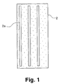
- Fig. 1 shows a configuration of the shadow mask 2 for the formation of the organic emissive layer 63 relating to the present embodiment.
- the conventional mask shown in Fig. 9 are discrete openings 2a corresponding to the respective pixels.
- openings 2a that are in common among adjacent pixels. More specifically, for a particular color, the R pixels, for example, the R pixel group is arranged linearly in a column.
- the opening 2a for forming the R pixels is also arranged linearly in a column so that the opening 2a is in common among adjacent pixels. This yields the opening 2a as a stripe shape as shown in the figure.
- the width of the opening 2a corresponds to the width of one pixel and the length is determined according to the number of pixels to be in common.
- the length of the organic emissive layer 63 in common with all the pixels arranged in the column is the pixel length ⁇ k.
- the pitch of the stripe shape opening 2a is equivalent to the pitch of the same color pixels in the row.
- the mask 2 has the same conventional thickness of 50 ⁇ m.
- the mask for the G pixels and the mask for the B pixels have a similar configuration and the opening 2a can be formed in a stripe shape.
- the organic emissive layer 63 for the R pixels, the organic emissive layer 63 for the G pixels, and the organic emissive layer 63 for the B pixels are respectively formed on the substrate 3.
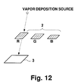
- the evaporation source is usually positioned below the substrate 3, and the mask 2 is positioned between the evaporation source and the substrate 3 (bottom surface of the substrate).
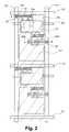
- Fig. 2 is a top view of the organic EL display when the organic emissive layer 63 is formed using the mask 2 shown in Fig. 1.
- Fig. 3A and 3B respectively show the cross-sectional views of A-A and B-B in Fig. 2. It should be noted that two adjacent pixels of the same color are shown in a column for the convenience of illustration.
- each pixel is substantially similar to that shown in Fig. 7.
- the thin-film transistors 13, 42 and the storage capacitor 70 are formed in one pixel.
- the drain of the thin-film transistor 13 is connected to the data line 52
- the source of the thin-film transistor 13 is connected to one electrode of the storage capacitor 70 and to the gate of the thin-film transistor 42
- the gate of the thin-film transistor 13 is connected to the gate line 51.
- the source of the thin-film transistor 42 is connected to the power line 53 and the drain is connected to the transparent anode 61.
- the mask 2 having the stripe-shaped openings 2a as shown in Fig. 1 is used so that the organic emissive layer 63 is formed not only on the electrode of one pixel, namely, the anode 61 individually formed as an electrode for each pixel, but integrally on all the adjacent pixels in the column, or more specifically, the column region sandwiched by the data line 52 and the power line 53.
- the formed region of the organic emissive layer 63 is shown shaded for convenience. It is formed not only on the anode 61 of one pixel but also on the thin-film transistors 13, 42, the storage capacitor 70, and the gate line 51.
- the organic emissive layer 63 is formed in a similar manner as the hole transport layer 62, the electron transport layer 64, and the cathode 66 in Fig. 3A, and the organic emissive layer 63 extends near a source electrode 43s of the thin-film transistor 42 in Fig. 3B.
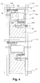
- the conventional formed region of the organic emissive layer 63 is shown shaded in Fig. 4.
- the organic emissive layer 63 is formed only on the anode 61 of one pixel, which clearly differs from the present embodiment.
- the opening 2a of the mask 2 has a striped shape and the organic emissive layer 63 is in common with adjacent pixels of the same color so that the edges of the opening 2a are not on a boundary of adjacent pixels or a boundary of the anode 61. Therefore, in the case where the organic emissive layer 63 is formed by evaporation, the shadowing effect at the edges disappears, and the film thickness of the organic emissive layer 63 can be made uniform along the column.
- the organic emissive layer 63 is formed also on the thin-film transistors 13, 42 and the storage capacitor 70.
- the organic emissive layer 63 has a high resistivity, current flows only through the part sandwiched by the anode 61 and the cathode 66 so that light emission occurs only on the anode 61. Namely, light emission occurs at each pixel.
- the present embodiment was described for the case where pixels of the same color are linearly arranged along a column.
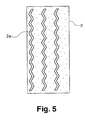
- the invention can also be applied for the case where pixels of the same color are arranged in a zigzag manner along a column, such as in a delta arrangement.
- Fig. 5 shows the mask 2 for this case.
- the openings 2a are also formed in a zigzag shape along the column.
- Using this mask 2 enables the organic emissive layer 63 to be in common among the pixels of the same color in adjacency in a zigzag manner and the film thickness of the organic emissive layer 63 to be uniform on the anode 61.
- the organic emissive layer 63 can also be formed in common by an ink jet method in a similar fashion using the mask 2 (which functions as a frame for limiting the region for dripping ink) shown in Fig. 1.
- the mask 2 shown in Fig. 1 can be used for each panel.
- the present embodiment was described for the case in which the organic emissive layer 63 was formed using a mask.
- the hole transport layer 62, the organic emissive layer 63, and the electron transport layer 64 forming the organic layer 65 can also all be formed using the same mask.
- the present invention is also applicable in this case. Namely, by having the mask for forming the hole transport layer 62 in common with adjacent pixels, the hole transport layer 62 is in common with adjacent pixels of the same color. Then, as described above, by having the mask for forming the emissive layer 63 in common with adjacent pixels, the emissive layer 63 is in common with adjacent pixels of the same color.
- the electron transport layer 64 can be made in common with adjacent pixels of the same color.
- the hole transport layer 62 and the organic emissive layer 63 can be in common with adjacent pixels of the same color with the electron transport layer 64 formed at each pixel, or the hole transport layer 62 can be formed at each pixel with the organic emissive layer 63 and the electron transport layer 64 in common with adjacent pixels of the same color.
Landscapes
- Engineering & Computer Science (AREA)
- Microelectronics & Electronic Packaging (AREA)
- Manufacturing & Machinery (AREA)
- Electroluminescent Light Sources (AREA)
- Devices For Indicating Variable Information By Combining Individual Elements (AREA)
Applications Claiming Priority (2)
| Application Number | Priority Date | Filing Date | Title |
|---|---|---|---|
| JP2001102390A JP4789341B2 (ja) | 2001-03-30 | 2001-03-30 | 半導体装置及び半導体装置製造用マスク |
| JP2001102390 | 2001-03-30 |
Publications (2)
| Publication Number | Publication Date |
|---|---|
| EP1246246A2 true EP1246246A2 (de) | 2002-10-02 |
| EP1246246A3 EP1246246A3 (de) | 2005-10-26 |
Family
ID=18955599
Family Applications (1)
| Application Number | Title | Priority Date | Filing Date |
|---|---|---|---|
| EP02252386A Withdrawn EP1246246A3 (de) | 2001-03-30 | 2002-04-02 | Lichtemittierende Vorrichtung und Herstellungsverfahren |
Country Status (6)
| Country | Link |
|---|---|
| US (1) | US6975065B2 (de) |
| EP (1) | EP1246246A3 (de) |
| JP (1) | JP4789341B2 (de) |
| KR (1) | KR100462514B1 (de) |
| CN (1) | CN1384696A (de) |
| TW (1) | TWI286385B (de) |
Cited By (1)
| Publication number | Priority date | Publication date | Assignee | Title |
|---|---|---|---|---|
| WO2013160778A1 (en) * | 2012-04-25 | 2013-10-31 | Ignis Innovation Inc. | High resolution display architecture |
Families Citing this family (11)
| Publication number | Priority date | Publication date | Assignee | Title |
|---|---|---|---|---|
| KR100686343B1 (ko) | 2003-11-29 | 2007-02-22 | 삼성에스디아이 주식회사 | 유기 전계 발광 표시 장치 |
| CN1822385B (zh) | 2005-01-31 | 2013-02-06 | 株式会社半导体能源研究所 | 显示装置及含有其的电子设备 |
| KR100708147B1 (ko) * | 2005-03-14 | 2007-04-16 | 삼성전자주식회사 | 발광소자 클러스터 및 이를 채용한 직하발광형 백라이트유닛 및 액정표시장치 |
| KR101219036B1 (ko) | 2005-05-02 | 2013-01-07 | 삼성디스플레이 주식회사 | 유기 발광 표시 장치 |
| KR100993426B1 (ko) | 2008-11-10 | 2010-11-09 | 삼성모바일디스플레이주식회사 | 유기전계발광 표시 장치 및 그의 제조 방법 |
| KR101711191B1 (ko) * | 2010-10-28 | 2017-03-02 | 삼성디스플레이 주식회사 | 유기 발광 표시 장치 및 그 제조방법 |
| CN102497690B (zh) * | 2011-12-16 | 2016-03-16 | 信利半导体有限公司 | 一种oled照明器件 |
| CN103205687B (zh) * | 2012-01-16 | 2016-03-02 | 昆山允升吉光电科技有限公司 | 蒸镀掩模板及其制作方法 |
| KR200492239Y1 (ko) | 2015-04-27 | 2020-09-03 | 코웨이 주식회사 | 휴대용 살균수 분사기 |
| KR102062587B1 (ko) * | 2017-02-08 | 2020-01-13 | 삼성디스플레이 주식회사 | 표시 장치 |
| CN111384086B (zh) * | 2018-12-28 | 2023-04-18 | 广东聚华印刷显示技术有限公司 | 像素结构及显示屏 |
Family Cites Families (17)
| Publication number | Priority date | Publication date | Assignee | Title |
|---|---|---|---|---|
| US5822026A (en) * | 1994-02-17 | 1998-10-13 | Seiko Epson Corporation | Active matrix substrate and color liquid crystal display |
| US5952037A (en) * | 1995-03-13 | 1999-09-14 | Pioneer Electronic Corporation | Organic electroluminescent display panel and method for manufacturing the same |
| JP3719743B2 (ja) * | 1995-08-09 | 2005-11-24 | 株式会社日立製作所 | プラズマディスプレイパネル |
| JP3539597B2 (ja) * | 1995-10-13 | 2004-07-07 | ソニー株式会社 | 有機光学的素子及びその製造方法 |
| US5688551A (en) * | 1995-11-13 | 1997-11-18 | Eastman Kodak Company | Method of forming an organic electroluminescent display panel |
| JPH10289784A (ja) * | 1997-04-14 | 1998-10-27 | Mitsubishi Chem Corp | 有機電界発光素子 |
| JP3580092B2 (ja) * | 1997-08-21 | 2004-10-20 | セイコーエプソン株式会社 | アクティブマトリクス型表示装置 |
| TW420965B (en) * | 1998-07-14 | 2001-02-01 | Matsushita Electric Industrial Co Ltd | Dispersion-type electroluminescence element |
| DE19916745A1 (de) * | 1999-04-13 | 2000-10-19 | Mannesmann Vdo Ag | Lichtemittierende Diode mit organischen lichtemittierenden Stoffen zur Erzeugung von Licht mit Mischfarben |
| TW480722B (en) | 1999-10-12 | 2002-03-21 | Semiconductor Energy Lab | Manufacturing method of electro-optical device |
| JP4780826B2 (ja) * | 1999-10-12 | 2011-09-28 | 株式会社半導体エネルギー研究所 | 電気光学装置の作製方法 |
| JP2001313172A (ja) * | 2000-02-25 | 2001-11-09 | Seiko Epson Corp | 有機エレクトロルミネッセンス白色光源、及びその製造方法 |
| JP4601842B2 (ja) * | 2000-02-28 | 2010-12-22 | 株式会社半導体エネルギー研究所 | 薄膜形成方法 |
| TW495809B (en) * | 2000-02-28 | 2002-07-21 | Semiconductor Energy Lab | Thin film forming device, thin film forming method, and self-light emitting device |
| JP2001296819A (ja) * | 2000-04-17 | 2001-10-26 | Nec Corp | 有機薄膜elデバイス及びその製造方法 |
| JP4053209B2 (ja) * | 2000-05-01 | 2008-02-27 | 三星エスディアイ株式会社 | 有機elディスプレイの製造方法 |
| CN1295945C (zh) * | 2000-12-20 | 2007-01-17 | 皇家菲利浦电子有限公司 | 场致发光彩色显示屏 |
-
2001
- 2001-03-30 JP JP2001102390A patent/JP4789341B2/ja not_active Expired - Lifetime
-
2002
- 2002-03-06 TW TW091104103A patent/TWI286385B/zh not_active IP Right Cessation
- 2002-03-27 US US10/109,170 patent/US6975065B2/en not_active Expired - Lifetime
- 2002-03-29 CN CN02104991A patent/CN1384696A/zh active Pending
- 2002-03-29 KR KR10-2002-0017323A patent/KR100462514B1/ko not_active Expired - Lifetime
- 2002-04-02 EP EP02252386A patent/EP1246246A3/de not_active Withdrawn
Cited By (3)
| Publication number | Priority date | Publication date | Assignee | Title |
|---|---|---|---|---|
| WO2013160778A1 (en) * | 2012-04-25 | 2013-10-31 | Ignis Innovation Inc. | High resolution display architecture |
| US9190456B2 (en) | 2012-04-25 | 2015-11-17 | Ignis Innovation Inc. | High resolution display panel with emissive organic layers emitting light of different colors |
| USRE48002E1 (en) | 2012-04-25 | 2020-05-19 | Ignis Innovation Inc. | High resolution display panel with emissive organic layers emitting light of different colors |
Also Published As
| Publication number | Publication date |
|---|---|
| US20020158576A1 (en) | 2002-10-31 |
| TWI286385B (en) | 2007-09-01 |
| EP1246246A3 (de) | 2005-10-26 |
| KR20020077241A (ko) | 2002-10-11 |
| CN1384696A (zh) | 2002-12-11 |
| JP2002299052A (ja) | 2002-10-11 |
| US6975065B2 (en) | 2005-12-13 |
| KR100462514B1 (ko) | 2004-12-17 |
| JP4789341B2 (ja) | 2011-10-12 |
Similar Documents
| Publication | Publication Date | Title |
|---|---|---|
| US7432885B2 (en) | Active matrix display | |
| KR100518709B1 (ko) | 마스크를 사용해서 층 재료를 부착시켜 기판 상에 사전설정된 패턴의 층을 형성하는 방법 | |
| JP4624452B2 (ja) | カラー有機el表示装置 | |
| US20040135501A1 (en) | Organic electroluminescence panel | |
| US7190122B2 (en) | OLED display with improved active matrix circuitry | |
| KR20010050816A (ko) | 컬러 표시 장치 | |
| JP2001290441A (ja) | カラー表示装置 | |
| KR100545974B1 (ko) | 일렉트로 루미네센스 표시 장치 및 일렉트로 루미네센스표시 장치의 패턴 레이아웃 방법 | |
| CN111863881A (zh) | Oled显示装置及制造oled显示装置的方法 | |
| US6975065B2 (en) | Light-emitting device and light-emitting device manufacturing method | |
| US6380673B1 (en) | Organic electroluminescence display | |
| WO2007130289A2 (en) | Electrical connection in oled devices | |
| JP4260126B2 (ja) | カラー有機el表示装置 | |
| US20110241036A1 (en) | Light-emitting apparatus | |
| KR20060023180A (ko) | 유기 el 패널 및 그 제조 방법 | |
| US7256757B2 (en) | Organic EL display panel | |
| JP2006331920A (ja) | 蒸着マスク、有機エレクトロルミネッセンス表示装置、及び、その製造方法 | |
| JP4789340B2 (ja) | 半導体装置及び半導体装置製造用マスク | |
| WO2021126143A1 (en) | Oled sub-pixel patterning structure | |
| KR100902076B1 (ko) | 유기 전계 발광 장치의 화소 회로 및 그 제조방법 | |
| KR100550005B1 (ko) | 표면 발광형 유기 이엘 다이오드 디스플레이 장치 및 그제조 방법 | |
| KR100873066B1 (ko) | 유기 전계 발광 장치 및 그 제조방법 | |
| JP2002367776A (ja) | 有機エレクトロルミネセンス素子 | |
| JP2003066871A (ja) | 有機el表示装置及びその製造方法 |
Legal Events
| Date | Code | Title | Description |
|---|---|---|---|
| PUAI | Public reference made under article 153(3) epc to a published international application that has entered the european phase |
Free format text: ORIGINAL CODE: 0009012 |
|
| AK | Designated contracting states |
Kind code of ref document: A2 Designated state(s): AT BE CH CY DE DK ES FI FR GB GR IE IT LI LU MC NL PT SE TR |
|
| AX | Request for extension of the european patent |
Free format text: AL;LT;LV;MK;RO;SI |
|
| PUAL | Search report despatched |
Free format text: ORIGINAL CODE: 0009013 |
|
| AK | Designated contracting states |
Kind code of ref document: A3 Designated state(s): AT BE CH CY DE DK ES FI FR GB GR IE IT LI LU MC NL PT SE TR |
|
| AX | Request for extension of the european patent |
Extension state: AL LT LV MK RO SI |
|
| 17P | Request for examination filed |
Effective date: 20060313 |
|
| AKX | Designation fees paid |
Designated state(s): DE FI NL |
|
| STAA | Information on the status of an ep patent application or granted ep patent |
Free format text: STATUS: THE APPLICATION IS DEEMED TO BE WITHDRAWN |
|
| 18D | Application deemed to be withdrawn |
Effective date: 20061004 |