EP1246264A2 - Nitrid-Halbleitervorrichtung - Google Patents
Nitrid-Halbleitervorrichtung Download PDFInfo
- Publication number
- EP1246264A2 EP1246264A2 EP02006937A EP02006937A EP1246264A2 EP 1246264 A2 EP1246264 A2 EP 1246264A2 EP 02006937 A EP02006937 A EP 02006937A EP 02006937 A EP02006937 A EP 02006937A EP 1246264 A2 EP1246264 A2 EP 1246264A2
- Authority
- EP
- European Patent Office
- Prior art keywords
- nitride semiconductor
- layer
- semiconductor device
- contact
- contact layer
- Prior art date
- Legal status (The legal status is an assumption and is not a legal conclusion. Google has not performed a legal analysis and makes no representation as to the accuracy of the status listed.)
- Withdrawn
Links
Images


Classifications
-
- H—ELECTRICITY
- H10—SEMICONDUCTOR DEVICES; ELECTRIC SOLID-STATE DEVICES NOT OTHERWISE PROVIDED FOR
- H10H—INORGANIC LIGHT-EMITTING SEMICONDUCTOR DEVICES HAVING POTENTIAL BARRIERS
- H10H20/00—Individual inorganic light-emitting semiconductor devices having potential barriers, e.g. light-emitting diodes [LED]
- H10H20/80—Constructional details
- H10H20/81—Bodies
- H10H20/822—Materials of the light-emitting regions
- H10H20/824—Materials of the light-emitting regions comprising only Group III-V materials, e.g. GaP
- H10H20/825—Materials of the light-emitting regions comprising only Group III-V materials, e.g. GaP containing nitrogen, e.g. GaN
-
- B—PERFORMING OPERATIONS; TRANSPORTING
- B82—NANOTECHNOLOGY
- B82Y—SPECIFIC USES OR APPLICATIONS OF NANOSTRUCTURES; MEASUREMENT OR ANALYSIS OF NANOSTRUCTURES; MANUFACTURE OR TREATMENT OF NANOSTRUCTURES
- B82Y20/00—Nanooptics, e.g. quantum optics or photonic crystals
-
- H—ELECTRICITY
- H01—ELECTRIC ELEMENTS
- H01S—DEVICES USING THE PROCESS OF LIGHT AMPLIFICATION BY STIMULATED EMISSION OF RADIATION [LASER] TO AMPLIFY OR GENERATE LIGHT; DEVICES USING STIMULATED EMISSION OF ELECTROMAGNETIC RADIATION IN WAVE RANGES OTHER THAN OPTICAL
- H01S5/00—Semiconductor lasers
- H01S5/30—Structure or shape of the active region; Materials used for the active region
- H01S5/34—Structure or shape of the active region; Materials used for the active region comprising quantum well or superlattice structures, e.g. single quantum well [SQW] lasers, multiple quantum well [MQW] lasers or graded index separate confinement heterostructure [GRINSCH] lasers
- H01S5/343—Structure or shape of the active region; Materials used for the active region comprising quantum well or superlattice structures, e.g. single quantum well [SQW] lasers, multiple quantum well [MQW] lasers or graded index separate confinement heterostructure [GRINSCH] lasers in AIIIBV compounds, e.g. AlGaAs-laser, InP-based laser
- H01S5/34333—Structure or shape of the active region; Materials used for the active region comprising quantum well or superlattice structures, e.g. single quantum well [SQW] lasers, multiple quantum well [MQW] lasers or graded index separate confinement heterostructure [GRINSCH] lasers in AIIIBV compounds, e.g. AlGaAs-laser, InP-based laser with a well layer based on Ga(In)N or Ga(In)P, e.g. blue laser
-
- H—ELECTRICITY
- H01—ELECTRIC ELEMENTS
- H01S—DEVICES USING THE PROCESS OF LIGHT AMPLIFICATION BY STIMULATED EMISSION OF RADIATION [LASER] TO AMPLIFY OR GENERATE LIGHT; DEVICES USING STIMULATED EMISSION OF ELECTROMAGNETIC RADIATION IN WAVE RANGES OTHER THAN OPTICAL
- H01S2304/00—Special growth methods for semiconductor lasers
-
- H—ELECTRICITY
- H01—ELECTRIC ELEMENTS
- H01S—DEVICES USING THE PROCESS OF LIGHT AMPLIFICATION BY STIMULATED EMISSION OF RADIATION [LASER] TO AMPLIFY OR GENERATE LIGHT; DEVICES USING STIMULATED EMISSION OF ELECTROMAGNETIC RADIATION IN WAVE RANGES OTHER THAN OPTICAL
- H01S5/00—Semiconductor lasers
- H01S5/04—Processes or apparatus for excitation, e.g. pumping, e.g. by electron beams
- H01S5/042—Electrical excitation ; Circuits therefor
- H01S5/0425—Electrodes, e.g. characterised by the structure
- H01S5/04256—Electrodes, e.g. characterised by the structure characterised by the configuration
- H01S5/04257—Electrodes, e.g. characterised by the structure characterised by the configuration having positive and negative electrodes on the same side of the substrate
-
- H—ELECTRICITY
- H01—ELECTRIC ELEMENTS
- H01S—DEVICES USING THE PROCESS OF LIGHT AMPLIFICATION BY STIMULATED EMISSION OF RADIATION [LASER] TO AMPLIFY OR GENERATE LIGHT; DEVICES USING STIMULATED EMISSION OF ELECTROMAGNETIC RADIATION IN WAVE RANGES OTHER THAN OPTICAL
- H01S5/00—Semiconductor lasers
- H01S5/30—Structure or shape of the active region; Materials used for the active region
- H01S5/305—Structure or shape of the active region; Materials used for the active region characterised by the doping materials used in the laser structure
- H01S5/3054—Structure or shape of the active region; Materials used for the active region characterised by the doping materials used in the laser structure p-doping
- H01S5/3063—Structure or shape of the active region; Materials used for the active region characterised by the doping materials used in the laser structure p-doping using Mg
-
- H—ELECTRICITY
- H10—SEMICONDUCTOR DEVICES; ELECTRIC SOLID-STATE DEVICES NOT OTHERWISE PROVIDED FOR
- H10H—INORGANIC LIGHT-EMITTING SEMICONDUCTOR DEVICES HAVING POTENTIAL BARRIERS
- H10H20/00—Individual inorganic light-emitting semiconductor devices having potential barriers, e.g. light-emitting diodes [LED]
- H10H20/80—Constructional details
- H10H20/83—Electrodes
- H10H20/832—Electrodes characterised by their material
Definitions
- the present invention relates to a group III nitride semiconductor device, and more particularly, to an improvement of the electric contact properties between a semiconductor and metal electrodes of a group III nitride semiconductor device.
- semiconductor light emitting devices having a crystal layer of a group III nitride semiconductor (Al x Ga 1-x ) 1-y In y N (0 ⁇ x ⁇ 1, 0 ⁇ y ⁇ 1) doped with a group II element such as magnesium (Mg), zinc (Zn) and the like are attracting attention as devices capable of emitting blue light. It is particularly required to develop a group III nitride semiconductor device having improved electric contact properties between electrodes and the semiconductor.
- a charge transportation on a p-type semiconductor/metal boundary basically depends on an energy difference between the valence band of the semiconductor and the Fermi level of the metal. Depending on the energy difference, an ohmic contact or a Schottky contact is formed.
- an ohmic contact or a Schottky contact is formed.
- there is no metal which sufficiently reduces the Schottky barrier for a p-type nitride semiconductor there is no metal which sufficiently reduces the Schottky barrier for a p-type nitride semiconductor, and further improvements in the contact properties cannot be attained by simply selecting an optimum electrode metal.
- a conventional method uses a semiconductor layer having a small band gap as a contact layer with a metal.
- Japanese Patent Kokai No. Hei 10-65216 discloses an attempt to reduce a contact resistance with electrodes by using a nitride semiconductor including In, having a small band gap, as a contact layer with the electrodes.
- a method for improving the contact properties by using a semiconductor layer having a high carrier concentration for a contact layer with a metal is also known.
- the foregoing method presents difficulties in achieving a high carrier density.
- AlGaN-based nitrides also suffer from their large band gap, and particularly with p-type ones, a high carrier concentration is difficult to achieve.
- the present invention has been made in view of the foregoing situation, and it is an object of the invention to provide a group III nitride semiconductor device having improved electrode contact properties of the device.
- a nitride semiconductor device is a nitride semiconductor device including a semiconductor layer made of a group III nitride semiconductor, and a metal electrode for supplying the semiconductor layer with a carrier, the device comprising:
- the second contact layer may have a group II element added thereto.
- the second contact layer may have a thickness of 500 ⁇ or less.
- the aforementioned group II element may be magnesium.
- the first contact layer may be In y Ga 1-y N (0.05 ⁇ y ⁇ 0.4).
- the first contact layer characteristically may have a thickness in a range of 10 to 1000 ⁇ .
- the nitride semiconductor device may be a light emitting device.
- the present inventors have conducted detailed experiments on the electrode contact properties of a device which includes a semiconductor layer made of a group III nitride, and a metal electrode for supplying carriers, i.e., holes to the semiconductor layer, with the intention of improving the electric characteristic of the device to reach the present invention.
- the device disclosed in the aforementioned Japanese Patent Kokai No. Hei 10-65216 was fabricated using a contact layer made of p-type InGaN which was provided with a high hole concentration through a thermal anneal treatment, and the device was investigated for the contact properties. However, no significant improvement was achieved.
- a thin GaN layer or the like was grown on the topmost surface as a second contact layer, and conversion into the p-type was effected by applying the thermal anneal treatment. This process was found to improve the contact properties of the completed device.
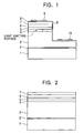
- Fig. 1 illustrates a semiconductor light emitting device having a multi-quantum well structure (MQW) according to the present invention.
- the device comprises a multi-layer structure having a plurality of nitride semiconductor crystal films represented by (Al x Ga 1-x ) 1-y In y N (0 ⁇ x ⁇ 1, 0 ⁇ y ⁇ 1), epitaxially grown in sequence on a substrate 1 made of sapphire.
- a low temperature buffer layer 2 made of AlN, GaN and the like, and an n-type GaN underlying layer 3 doped with Si or the like for growing a conductive layer are stacked in sequence.
- An active layer 4 is disposed on the n-type GaN underlying layer 3.
- Deposited in sequence on the active layer 4 are an Mg doped AlGaN electron barrier layer 5, an Mg doped InGaN layer 6, and an Mg-doped GaN layer 7, which are converted into the p-type through a thermal anneal treatment.
- An insulating layer 8 is further deposited on the p-type Mg-doped GaN layer 7 and n-type GaN underlying layer 3, and a p-side electrode 9 and an n-side electrode 10 are formed in corresponding windows, respectively, and a light emitting device is formed of the foregoing respective portions.
- an organic metal vapor deposition (MOCVD) method is used as a deposition method, unless otherwise indicated.
- a hydrogen gas is used as a gas for use in transportation of a precursor, unless otherwise indicated.
- a sapphire substrate 1 is loaded into an MOCVD reactor (not shown), and an AlN buffer layer 2 is grown on the sapphire substrate at low temperatures. Then, trimethyl gallium (TMG), ammonia and methyl silane are supplied to a reactor at flow rates of 1.7 x 10 -4 mol/minute, 9.0 x 10 -2 mol/minute, and 7.2 x 10 -9 mol/minute, respectively, to grow an n-type GaN layer 3 doped with Si in a thickness of approximately 6 ⁇ m, at a substrate temperature of 1050°C.
- TMG trimethyl gallium
- the substrate temperature is reduced to 780°C while ammonia is being supplied to the reactor at 9.0 x 10 -2 mol/minute.
- TMG is supplied at 4.8 x 10 -6 mol/minute; trimethyl indium (TMI) at 2.6 x 10 -5 mol/minute; and ammonia at 3.1 x 10 -1 mol/minute.
- TMG is supplied at 4.8 x 10 -6 mol/minute; TMI at 2.6 x 10 -6 mol/minute; and ammonia at 3.1 x 10 -1 mol/minute.
- TMG trimethyl aluminum
- EtCp2Mg bisethylcyclopentadienyl magnesium
- the substrate temperature is reduced to 770°C.
- TMG is supplied at 1.0 x 10 -5 mol/minute; TMI at 1.7 x 10 -5 mol/minute; EtCp2Mg at 8.8 x 10 -8 mol/minute; and ammonia at 4.5 x 10 -1 mol/minute to deposit an Mg doped InGaN layer 6.
- the supply of TMI is stopped, and the supply of EtCp2Mg is changed to 2.3 x 10 -7 mol/minute to grow an Mg doped GaN layer 7, i.e., a second contact layer of 10 ⁇ thick on the first contact layer 6, thereby completing a wafer 1 as illustrated in Fig. 2.
- the thickness is determined by epitaxially growing the second contact layer 7 for 40 seconds. The flow rate of EtCp2Mg is adjusted such that the hole concentration is maximized after thermal annealing in nitrogen, at 950°C, for 5 minutes.
- the total film thicknesses of the layers between the active layer and electrode e.g., the total thickness of GaN/InGaN (second contact layer 7/first contact layer 6) in the case of the wafer 1, are made the same with each other.
- each of the resulted wafers is thermally annealed in a nitrogen atmosphere at 950°C for 5 minutes.
- Mg which is a p-type dopant
- the n-type GaN layer 3 is exposed, as illustrated in Fig. 3, by reactive ion etching (RIE) or the like, by way of example.
- RIE reactive ion etching
- windows are patterned on the insulating film 8 for forming electrodes.
- a p-side electrode 9 and an n-side electrode 10 are formed, respectively, through the windows (Fig. 1).
- Suitable materials for the p-side electrode 9 and n-side electrode 10 are nickel and titanium, respectively.
- the rear surface of the sapphire substrate of each wafer is polished to reduce the wafer thickness to approximately 100 ⁇ m. Then, the wafer is cleaved into chips, thereby completing devices.
- the devices fabricated from the wafers 1, 2, 3 are hereinafter called the device 1, device 2 and device 3, respectively.
- Fig. 4 shows the electric characteristics including currents and voltages of the device 1 according to the embodiment of the present invention and the comparative devices 2 and 3. As is apparent from Fig. 4, a driving voltage is reduced by the present invention.
- the thickness of the second contact layer 7 is preferably 500 ⁇ or less.
- the thickness of the first contact layer 6 is preferably in a range of 10 to 1000 ⁇ .
- a ridge type semiconductor light emitting device may be formed as illustrated in Fig. 5, using the same technique as the foregoing embodiment, except that a guide layer and a cladding layer are newly provided.
- an n-type AlGaN cladding layer 11 and an n-type GaN guide layer 12 are stacked between an n-type GaN underlying layer 3 and an active layer 4, and a p-type GaN guide layer 13 and a p-type AlGaN cladding layer 14 are further stacked between a p-type Mg doped AlGaN electron barrier layer 5 and a p-type first contact layer 6.
- a mask of a predetermined width is formed on a second contact layer 7, and portions other than those below a mask, i.e., the p-type first contact layer 6, p-type second contact layer 7, and p-type AlGaN cladding layer 14 are removed, while leaving a portion of the whole thickness of the p-type GaN guide layer 13, thereby forming a narrow ridge structure.
- an insulating film 8 is formed on the resulting wafer, a p-side electrode window in a top portion of the ridge and an n-side electrode window are formed, and respective electrodes are disposed to fabricate a ridge type semiconductor light emitting device.
- Members indicated by the same reference numerals in Figs. 5 and 1 are the same members.
- a group III nitride semiconductor device has a first contact layer and a second contact layer between a semiconductor active layer and a metal electrode, the electrode contact properties of the device can be improved.
Landscapes
- Physics & Mathematics (AREA)
- Nanotechnology (AREA)
- Engineering & Computer Science (AREA)
- Chemical & Material Sciences (AREA)
- Optics & Photonics (AREA)
- Biophysics (AREA)
- Life Sciences & Earth Sciences (AREA)
- Electromagnetism (AREA)
- General Physics & Mathematics (AREA)
- Crystallography & Structural Chemistry (AREA)
- Condensed Matter Physics & Semiconductors (AREA)
- Led Devices (AREA)
- Semiconductor Lasers (AREA)
- Electrodes Of Semiconductors (AREA)
Applications Claiming Priority (2)
| Application Number | Priority Date | Filing Date | Title |
|---|---|---|---|
| JP2001092899 | 2001-03-28 | ||
| JP2001092899A JP2002289914A (ja) | 2001-03-28 | 2001-03-28 | 窒化物半導体素子 |
Publications (2)
| Publication Number | Publication Date |
|---|---|
| EP1246264A2 true EP1246264A2 (de) | 2002-10-02 |
| EP1246264A3 EP1246264A3 (de) | 2006-05-24 |
Family
ID=18947295
Family Applications (1)
| Application Number | Title | Priority Date | Filing Date |
|---|---|---|---|
| EP02006937A Withdrawn EP1246264A3 (de) | 2001-03-28 | 2002-03-26 | Nitrid-Halbleitervorrichtung |
Country Status (6)
| Country | Link |
|---|---|
| US (1) | US20020149026A1 (de) |
| EP (1) | EP1246264A3 (de) |
| JP (1) | JP2002289914A (de) |
| KR (1) | KR100475005B1 (de) |
| CN (1) | CN1379483A (de) |
| TW (1) | TW533606B (de) |
Families Citing this family (9)
| Publication number | Priority date | Publication date | Assignee | Title |
|---|---|---|---|---|
| CN1333470C (zh) * | 2004-02-27 | 2007-08-22 | 广镓光电股份有限公司 | 发光二极管结构 |
| CN1993835A (zh) * | 2004-06-14 | 2007-07-04 | 三菱电线工业株式会社 | 氮化物半导体发光器件 |
| JP2007188990A (ja) * | 2006-01-12 | 2007-07-26 | Mitsubishi Electric Corp | 窒化物半導体素子 |
| KR101337615B1 (ko) | 2006-06-26 | 2013-12-06 | 재단법인서울대학교산학협력재단 | 질화갈륨계 화합물 반도체 및 그 제조방법 |
| CN101931036B (zh) * | 2010-07-21 | 2014-03-12 | 中国科学院半导体研究所 | 一种氮化镓系发光二极管 |
| JP5598437B2 (ja) * | 2011-07-12 | 2014-10-01 | 豊田合成株式会社 | Iii族窒化物半導体発光素子の製造方法 |
| WO2014002959A1 (ja) * | 2012-06-25 | 2014-01-03 | 三菱化学株式会社 | m面窒化物系発光ダイオードの製造方法 |
| CN111640836A (zh) * | 2020-06-18 | 2020-09-08 | 佛山紫熙慧众科技有限公司 | GaN基LED器件电极结构及LED器件 |
| CN114242860B (zh) * | 2021-12-27 | 2024-11-26 | 江苏第三代半导体研究院有限公司 | Led芯片及其制备方法 |
Family Cites Families (9)
| Publication number | Priority date | Publication date | Assignee | Title |
|---|---|---|---|---|
| US5656832A (en) * | 1994-03-09 | 1997-08-12 | Kabushiki Kaisha Toshiba | Semiconductor heterojunction device with ALN buffer layer of 3nm-10nm average film thickness |
| JP2666237B2 (ja) * | 1994-09-20 | 1997-10-22 | 豊田合成株式会社 | 3族窒化物半導体発光素子 |
| JPH1051070A (ja) * | 1996-07-29 | 1998-02-20 | Fujitsu Ltd | 半導体レーザ |
| JP3374737B2 (ja) * | 1997-01-09 | 2003-02-10 | 日亜化学工業株式会社 | 窒化物半導体素子 |
| JP3322179B2 (ja) * | 1997-08-25 | 2002-09-09 | 松下電器産業株式会社 | 窒化ガリウム系半導体発光素子 |
| JPH1187850A (ja) * | 1997-09-03 | 1999-03-30 | Sharp Corp | 窒化物系化合物半導体レーザ素子及びレーザ装置 |
| JPH11251685A (ja) * | 1998-03-05 | 1999-09-17 | Toshiba Corp | 半導体レーザ |
| CA2322490C (en) * | 1998-03-12 | 2010-10-26 | Nichia Chemical Industries, Ltd. | Nitride semiconductor device |
| JP4149054B2 (ja) * | 1998-11-27 | 2008-09-10 | シャープ株式会社 | 半導体装置 |
-
2001
- 2001-03-28 JP JP2001092899A patent/JP2002289914A/ja active Pending
-
2002
- 2002-03-26 EP EP02006937A patent/EP1246264A3/de not_active Withdrawn
- 2002-03-26 US US10/105,633 patent/US20020149026A1/en not_active Abandoned
- 2002-03-27 TW TW091106078A patent/TW533606B/zh not_active IP Right Cessation
- 2002-03-28 CN CN02108234A patent/CN1379483A/zh active Pending
- 2002-03-28 KR KR10-2002-0017054A patent/KR100475005B1/ko not_active Expired - Fee Related
Also Published As
| Publication number | Publication date |
|---|---|
| EP1246264A3 (de) | 2006-05-24 |
| KR20020077194A (ko) | 2002-10-11 |
| KR100475005B1 (ko) | 2005-03-08 |
| JP2002289914A (ja) | 2002-10-04 |
| US20020149026A1 (en) | 2002-10-17 |
| TW533606B (en) | 2003-05-21 |
| CN1379483A (zh) | 2002-11-13 |
Similar Documents
| Publication | Publication Date | Title |
|---|---|---|
| US8513694B2 (en) | Nitride semiconductor device and manufacturing method of the device | |
| US6829273B2 (en) | Nitride semiconductor layer structure and a nitride semiconductor laser incorporating a portion of same | |
| US6020602A (en) | GaN based optoelectronic device and method for manufacturing the same | |
| US8304790B2 (en) | Nitride semiconductor with active layer of quantum well structure with indium-containing nitride semiconductor | |
| EP2383846B1 (de) | Lichtemissionsvorrichtung und Herstellungsverfahren dafür | |
| KR100735934B1 (ko) | 선택적으로 도핑된 ⅲ-ⅴ 질화물층을 갖는 디바이스 및 발광 디바이스 | |
| US8017932B2 (en) | Light-emitting device | |
| KR100448662B1 (ko) | 질화물반도체소자 및 그 제조방법 | |
| US7939833B2 (en) | Nitride semiconductor light emitting device | |
| US20120205625A1 (en) | (Al, In, Ga, B)N DEVICE STRUCTURES ON A PATTERNED SUBSTRATE | |
| US8357607B2 (en) | Method for fabricating nitride-based semiconductor device having electrode on m-plane | |
| US20070176162A1 (en) | Nitride semiconductor light-emitting device and method for manufacturing the same | |
| EP1196971B1 (de) | Nitrid-halbleiterschichtenstruktur und deren anwendung in halbleiterlasern | |
| US8030680B2 (en) | Nitride semiconductor light-emitting device and method for manufacturing the same | |
| WO2007060931A1 (ja) | 窒化物半導体素子 | |
| US20150115220A1 (en) | (Al, In, Ga, B)N DEVICE STRUCTURES ON A PATTERNED SUBSTRATE | |
| JPH1174622A (ja) | 窒化物系半導体発光素子 | |
| EP1246264A2 (de) | Nitrid-Halbleitervorrichtung | |
| JP2010040692A (ja) | 窒化物系半導体素子及びその製造方法 | |
| US7015515B2 (en) | Group III nitride compound semiconductor device having a superlattice structure | |
| JPH09167857A (ja) | 半導体素子及びその製造方法 | |
| JP3859356B2 (ja) | 窒化物半導体素子の製造方法 | |
| JP2004104088A (ja) | 窒化物半導体素子 | |
| JP2008277867A (ja) | 半導体発光素子の製造方法 | |
| JPH077182A (ja) | 窒化ガリウム系化合物半導体発光素子 |
Legal Events
| Date | Code | Title | Description |
|---|---|---|---|
| PUAI | Public reference made under article 153(3) epc to a published international application that has entered the european phase |
Free format text: ORIGINAL CODE: 0009012 |
|
| AK | Designated contracting states |
Kind code of ref document: A2 Designated state(s): AT BE CH CY DE DK ES FI FR GB GR IE IT LI LU MC NL PT SE TR |
|
| AX | Request for extension of the european patent |
Free format text: AL;LT;LV;MK;RO;SI |
|
| PUAL | Search report despatched |
Free format text: ORIGINAL CODE: 0009013 |
|
| AK | Designated contracting states |
Kind code of ref document: A3 Designated state(s): AT BE CH CY DE DK ES FI FR GB GR IE IT LI LU MC NL PT SE TR |
|
| AX | Request for extension of the european patent |
Extension state: AL LT LV MK RO SI |
|
| AKX | Designation fees paid | ||
| STAA | Information on the status of an ep patent application or granted ep patent |
Free format text: STATUS: THE APPLICATION IS DEEMED TO BE WITHDRAWN |
|
| 18D | Application deemed to be withdrawn |
Effective date: 20061127 |
|
| REG | Reference to a national code |
Ref country code: DE Ref legal event code: 8566 |