EP1248148A1 - Lithographische Maske mit Schutzschicht - Google Patents
Lithographische Maske mit Schutzschicht Download PDFInfo
- Publication number
- EP1248148A1 EP1248148A1 EP20010303222 EP01303222A EP1248148A1 EP 1248148 A1 EP1248148 A1 EP 1248148A1 EP 20010303222 EP20010303222 EP 20010303222 EP 01303222 A EP01303222 A EP 01303222A EP 1248148 A1 EP1248148 A1 EP 1248148A1
- Authority
- EP
- European Patent Office
- Prior art keywords
- layer
- mask
- substrate
- patterning means
- radiation
- Prior art date
- Legal status (The legal status is an assumption and is not a legal conclusion. Google has not performed a legal analysis and makes no representation as to the accuracy of the status listed.)
- Withdrawn
Links
- 238000001459 lithography Methods 0.000 title description 3
- 239000011241 protective layer Substances 0.000 title 1
- 238000000059 patterning Methods 0.000 claims abstract description 24
- 238000000034 method Methods 0.000 claims abstract description 16
- 229910010272 inorganic material Inorganic materials 0.000 claims abstract description 14
- 239000011147 inorganic material Substances 0.000 claims abstract description 14
- 238000004519 manufacturing process Methods 0.000 claims abstract description 14
- 239000000758 substrate Substances 0.000 claims description 34
- VYPSYNLAJGMNEJ-UHFFFAOYSA-N Silicium dioxide Chemical compound O=[Si]=O VYPSYNLAJGMNEJ-UHFFFAOYSA-N 0.000 claims description 20
- 229910052681 coesite Inorganic materials 0.000 claims description 10
- 229910052906 cristobalite Inorganic materials 0.000 claims description 10
- 239000000377 silicon dioxide Substances 0.000 claims description 10
- 229910052682 stishovite Inorganic materials 0.000 claims description 10
- 229910052905 tridymite Inorganic materials 0.000 claims description 10
- 239000000463 material Substances 0.000 claims description 6
- 229910052581 Si3N4 Inorganic materials 0.000 claims description 5
- 229910001632 barium fluoride Inorganic materials 0.000 claims description 5
- WUKWITHWXAAZEY-UHFFFAOYSA-L calcium difluoride Chemical compound [F-].[F-].[Ca+2] WUKWITHWXAAZEY-UHFFFAOYSA-L 0.000 claims description 5
- 229910001634 calcium fluoride Inorganic materials 0.000 claims description 5
- 238000000151 deposition Methods 0.000 claims description 2
- 230000005855 radiation Effects 0.000 abstract description 31
- 239000000356 contaminant Substances 0.000 abstract description 6
- 239000010410 layer Substances 0.000 description 63
- XUIMIQQOPSSXEZ-UHFFFAOYSA-N Silicon Chemical compound [Si] XUIMIQQOPSSXEZ-UHFFFAOYSA-N 0.000 description 13
- 229910052710 silicon Inorganic materials 0.000 description 13
- 239000010703 silicon Substances 0.000 description 13
- PZNSFCLAULLKQX-UHFFFAOYSA-N Boron nitride Chemical compound N#B PZNSFCLAULLKQX-UHFFFAOYSA-N 0.000 description 7
- QTBSBXVTEAMEQO-UHFFFAOYSA-N Acetic acid Chemical compound CC(O)=O QTBSBXVTEAMEQO-UHFFFAOYSA-N 0.000 description 5
- 229910052582 BN Inorganic materials 0.000 description 5
- 230000004075 alteration Effects 0.000 description 5
- 238000005530 etching Methods 0.000 description 5
- 230000003287 optical effect Effects 0.000 description 5
- QGZKDVFQNNGYKY-UHFFFAOYSA-N Ammonia Chemical compound N QGZKDVFQNNGYKY-UHFFFAOYSA-N 0.000 description 3
- 238000010894 electron beam technology Methods 0.000 description 3
- 230000033001 locomotion Effects 0.000 description 3
- 239000002245 particle Substances 0.000 description 3
- GRYLNZFGIOXLOG-UHFFFAOYSA-N Nitric acid Chemical compound O[N+]([O-])=O GRYLNZFGIOXLOG-UHFFFAOYSA-N 0.000 description 2
- 238000003486 chemical etching Methods 0.000 description 2
- 150000001875 compounds Chemical class 0.000 description 2
- 238000009826 distribution Methods 0.000 description 2
- 238000003384 imaging method Methods 0.000 description 2
- 238000010884 ion-beam technique Methods 0.000 description 2
- 229910017604 nitric acid Inorganic materials 0.000 description 2
- 230000010363 phase shift Effects 0.000 description 2
- 238000001020 plasma etching Methods 0.000 description 2
- TXEYQDLBPFQVAA-UHFFFAOYSA-N tetrafluoromethane Chemical compound FC(F)(F)F TXEYQDLBPFQVAA-UHFFFAOYSA-N 0.000 description 2
- KRHYYFGTRYWZRS-UHFFFAOYSA-N Fluorane Chemical compound F KRHYYFGTRYWZRS-UHFFFAOYSA-N 0.000 description 1
- 238000001015 X-ray lithography Methods 0.000 description 1
- 239000003929 acidic solution Substances 0.000 description 1
- 229910021529 ammonia Inorganic materials 0.000 description 1
- 238000003491 array Methods 0.000 description 1
- QVGXLLKOCUKJST-UHFFFAOYSA-N atomic oxygen Chemical compound [O] QVGXLLKOCUKJST-UHFFFAOYSA-N 0.000 description 1
- 230000002238 attenuated effect Effects 0.000 description 1
- 230000005540 biological transmission Effects 0.000 description 1
- 238000006243 chemical reaction Methods 0.000 description 1
- 238000005229 chemical vapour deposition Methods 0.000 description 1
- 239000011248 coating agent Substances 0.000 description 1
- 238000000576 coating method Methods 0.000 description 1
- 230000003750 conditioning effect Effects 0.000 description 1
- 238000010276 construction Methods 0.000 description 1
- 238000013461 design Methods 0.000 description 1
- 238000001514 detection method Methods 0.000 description 1
- 238000011161 development Methods 0.000 description 1
- 230000000694 effects Effects 0.000 description 1
- 230000005670 electromagnetic radiation Effects 0.000 description 1
- 238000005516 engineering process Methods 0.000 description 1
- 239000007789 gas Substances 0.000 description 1
- PCHJSUWPFVWCPO-UHFFFAOYSA-N gold Chemical compound [Au] PCHJSUWPFVWCPO-UHFFFAOYSA-N 0.000 description 1
- 229910052737 gold Inorganic materials 0.000 description 1
- 239000010931 gold Substances 0.000 description 1
- 150000004678 hydrides Chemical class 0.000 description 1
- 238000005286 illumination Methods 0.000 description 1
- 238000007689 inspection Methods 0.000 description 1
- 238000005468 ion implantation Methods 0.000 description 1
- 239000002346 layers by function Substances 0.000 description 1
- 239000004973 liquid crystal related substance Substances 0.000 description 1
- 230000005381 magnetic domain Effects 0.000 description 1
- 239000011159 matrix material Substances 0.000 description 1
- 238000005259 measurement Methods 0.000 description 1
- 230000015654 memory Effects 0.000 description 1
- QSHDDOUJBYECFT-UHFFFAOYSA-N mercury Chemical compound [Hg] QSHDDOUJBYECFT-UHFFFAOYSA-N 0.000 description 1
- 229910052753 mercury Inorganic materials 0.000 description 1
- 238000001465 metallisation Methods 0.000 description 1
- 239000000203 mixture Substances 0.000 description 1
- 229910000069 nitrogen hydride Inorganic materials 0.000 description 1
- 239000012044 organic layer Substances 0.000 description 1
- 239000011368 organic material Substances 0.000 description 1
- 230000003647 oxidation Effects 0.000 description 1
- 238000007254 oxidation reaction Methods 0.000 description 1
- 239000001301 oxygen Substances 0.000 description 1
- 229910052760 oxygen Inorganic materials 0.000 description 1
- 238000005240 physical vapour deposition Methods 0.000 description 1
- 238000005498 polishing Methods 0.000 description 1
- 229920001721 polyimide Polymers 0.000 description 1
- 229920000642 polymer Polymers 0.000 description 1
- 230000037452 priming Effects 0.000 description 1
- 238000012545 processing Methods 0.000 description 1
- 239000004065 semiconductor Substances 0.000 description 1
- 238000007493 shaping process Methods 0.000 description 1
- 238000003860 storage Methods 0.000 description 1
- 239000010409 thin film Substances 0.000 description 1
Images


Classifications
-
- G—PHYSICS
- G03—PHOTOGRAPHY; CINEMATOGRAPHY; ANALOGOUS TECHNIQUES USING WAVES OTHER THAN OPTICAL WAVES; ELECTROGRAPHY; HOLOGRAPHY
- G03F—PHOTOMECHANICAL PRODUCTION OF TEXTURED OR PATTERNED SURFACES, e.g. FOR PRINTING, FOR PROCESSING OF SEMICONDUCTOR DEVICES; MATERIALS THEREFOR; ORIGINALS THEREFOR; APPARATUS SPECIALLY ADAPTED THEREFOR
- G03F1/00—Originals for photomechanical production of textured or patterned surfaces, e.g., masks, photo-masks, reticles; Mask blanks or pellicles therefor; Containers specially adapted therefor; Preparation thereof
- G03F1/62—Pellicles, e.g. pellicle assemblies, e.g. having membrane on support frame; Preparation thereof
-
- G—PHYSICS
- G03—PHOTOGRAPHY; CINEMATOGRAPHY; ANALOGOUS TECHNIQUES USING WAVES OTHER THAN OPTICAL WAVES; ELECTROGRAPHY; HOLOGRAPHY
- G03F—PHOTOMECHANICAL PRODUCTION OF TEXTURED OR PATTERNED SURFACES, e.g. FOR PRINTING, FOR PROCESSING OF SEMICONDUCTOR DEVICES; MATERIALS THEREFOR; ORIGINALS THEREFOR; APPARATUS SPECIALLY ADAPTED THEREFOR
- G03F1/00—Originals for photomechanical production of textured or patterned surfaces, e.g., masks, photo-masks, reticles; Mask blanks or pellicles therefor; Containers specially adapted therefor; Preparation thereof
- G03F1/62—Pellicles, e.g. pellicle assemblies, e.g. having membrane on support frame; Preparation thereof
- G03F1/64—Pellicles, e.g. pellicle assemblies, e.g. having membrane on support frame; Preparation thereof characterised by the frames, e.g. structure or material, including bonding means therefor
Definitions
- the present invention relates to patterning means for use in a lithographic projection apparatus comprising a patterned layer, a frame and a protecting layer having a thickness of less than 10 ⁇ m.
- the apparatus usually comprises:
- patterning means as here employed should be broadly interpreted as referring to means that can be used to endow an incoming radiation beam with a patterned cross-section, corresponding to a pattern that is to be created in a target portion of the substrate; the term “light valve” can also be used in this context.
- the said pattern will correspond to a particular functional layer in a device being created in the target portion, such as an integrated circuit or other device (see below). Examples of such patterning means include:
- Lithographic projection apparatus can be used, for example, in the manufacture of integrated circuits (ICs).
- the patterning means may generate a circuit pattern corresponding to an individual layer of the IC, and this pattern can be imaged onto a target portion (e.g. comprising one or more dies) on a substrate (silicon wafer) that has been coated with a layer of radiation-sensitive material (resist).
- a target portion e.g. comprising one or more dies
- a substrate silicon wafer
- a layer of radiation-sensitive material resist
- a single wafer will contain a whole network of adjacent target portions that are successively irradiated via the projection system, one at a time.
- employing patterning by a mask on a mask table a distinction can be made between two different types of machine.
- each target portion is irradiated by exposing the entire mask pattern onto the target portion in one go; such an apparatus is commonly referred to as a wafer stepper.
- each target portion is irradiated by progressively scanning the mask pattern under the projection beam in a given reference direction (the "scanning" direction) while synchronously scanning the substrate table parallel or anti-parallel to this direction; since, in general, the projection system will have a magnification factor M (generally ⁇ 1), the speed V at which the substrate table is scanned will be a factor M times that at which the mask table is scanned.
- M magnification factor
- a pattern (e.g. in a mask) is imaged onto a substrate that is at least partially covered by a layer of radiation-sensitive material (resist).
- the substrate Prior to this imaging step, the substrate may undergo various procedures, such as priming, resist coating and a soft bake. After exposure, the substrate may be subjected to other procedures, such as a post-exposure bake (PEB), development, a hard bake and measurement/inspection of the imaged features.
- PEB post-exposure bake
- This array of procedures is used as a basis to pattern an individual layer of a device, e.g. an IC.
- Such a patterned layer may then undergo various processes such as etching, ion-implantation (doping), metallization, oxidation, chemo-mechanical polishing, etc., all intended to finish off an individual layer. If several layers are required, then the whole procedure, or a variant thereof, will have to be repeated for each new layer. Eventually, an array of devices will be present on the substrate (wafer). These devices are then separated from one another by a technique such as dicing or sawing, whence the individual devices can be mounted on a carrier, connected to pins, etc.
- the projection system may hereinafter be referred to as the "lens"; however, this term should be broadly interpreted as encompassing various types of projection system, including refractive optics, reflective optics, and catadioptric systems, for example.
- the radiation system may also include components operating according to any of these design types for directing, shaping or controlling the projection beam of radiation, and such components may also be referred to below, collectively or singularly, as a "lens”.
- the lithographic apparatus may be of a type having two or more substrate tables (and/or two or more mask tables). In such "multiple stage” devices the additional tables may be used in parallel, or preparatory steps may be carried out on one or more tables while one or more other tables are being used for exposures. Twin stage lithographic apparatus are described, for example, in US 5,969,441 and WO 98/40791, incorporated herein by reference.
- lithographic projection apparatus employ patterning means comprising the patterned layer in order to endow the projection beam with the pattern in its cross-section.
- the pattern (which is part of the patterned layer) is positioned in a focal plane position in order to properly image the pattern onto a target portion of the substrate.
- Contaminants such as particles or adsorbing (carbonaceous) species, may foul the pattern of the patterned layer.
- the patterning means comprises a protecting layer. This protecting layer keeps contaminants out of the focal plane position, hence not affecting the imaged pattern.
- this layer In the case of a relatively thick protecting layer having a thickness of about 300 to 1000 ⁇ m, this layer generally acts as an optical element, consequently introducing aberrations. These aberrations become particularly significant if 157 nm radiation is employed as opposed to 248 and 193 nm radiation. In such case, aberrations may, for example, cause a drift in the focal plane position or introduce a shift of the imaged pattern in the plane of the substrate surface. Moreover, during a scanning motion the protecting layer may vibrate perpendicular to the plane of the layer. The vibrating movement of the protecting layer leads to variation in aberration level, which is very hard, if not impossible, to correct.
- protecting layers having a thickness of a few microns are contemplated. These layers do not act as optical elements and hence will not introduce aforementioned aberrations. In general, such thin layers are difficult to manufacture. For this reason, protecting layers consisting of organic materials are being manufactured today and considered for use in lithography. However, such organic layers have as a disadvantage that they are generally not sufficiently transparent to 157 nm radiation. And above all, these layers are not stable upon exposure to 157 nm radiation and deteriorate in a short period of time.
- patterning means as specified in the opening paragraph, which patterning means can be characterized in that the protecting layer comprises an inorganic material.
- Such inorganic material can be manufactured sufficiently thin and appeared to be stable upon exposure to 157 nm radiation.
- Suitable inorganic materials that are transmissive to 157 nm radiation may be selected from a group comprising SiO 2 , F-doped SiO 2 , CaF 2 , BaF 2 , BN and Si 3 N 4 .
- a method of manufacturing a patterning means comprising a patterned layer, a frame and a protecting layer having a thickness of less than 10 ⁇ m, the method comprising the steps of:
- a method to manufacture a mask for x-ray lithography is proposed in which a thin boron nitride (BN) layer is manufactured.
- the BN layer acts as supporting layer for bearing the pattern of the mask.
- This layer does not stand-alone; on top of the BN layer a polymer e . g . polyimide film is deposited, onto which a pattern consisting of gold, for example, is provided.
- a polymer e . g . polyimide film is deposited, onto which a pattern consisting of gold, for example, is provided.
- More details can be gleaned from S.S. Dana and J.R. Maldonado, J. Vacuum Science and Technology, B4 (1), 1986, 235-239, which is incorporated herein by reference.
- the present invention only one inorganic layer is required for protecting the pattern on the patterned layer.
- the method must also be suitable for other inorganic materials. As a consequence, for each material specific manufacturing conditions are needed.
- the terms "radiation” and “beam” are used to encompass all types of electromagnetic radiation, including ultraviolet radiation (e.g. with a wavelength of 365, 248, 193, 157 or 126 nm) and EUV (extreme ultra-violet radiation, e.g. having a wavelength in the range 5-20 nm), as well as particle beams, such as ion beams or electron beams.
- ultraviolet radiation e.g. with a wavelength of 365, 248, 193, 157 or 126 nm
- EUV extreme ultra-violet radiation, e.g. having a wavelength in the range 5-20 nm
- particle beams such as ion beams or electron beams.
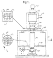
- Figure 1 schematically depicts a lithographic projection apparatus according to a particular embodiment of the invention.
- the apparatus comprises:
- the source LA (e.g. an excimer laser, an undulator or wiggler provided around the path of an electron beam in a storage ring or synchrotron, a laser-produced plasma source, a discharge source or an electron or ion beam source) produces a beam of radiation.
- This beam is fed into an illumination system (illuminator) IL, either directly or after having traversed conditioning means, such as a beam expander Ex, for example.
- the illuminator IL may comprise adjusting means AM for setting the outer and/or inner radial extent (commonly referred to as ⁇ -outer and ⁇ -inner, respectively) of the intensity distribution in the beam.
- it will generally comprise various other components, such as an integrator IN and a condenser CO.
- the beam PB impinging on the mask MA has a desired uniformity and intensity distribution in its cross-section.
- the source LA may be within the housing of the lithographic projection apparatus (as is often the case when the source LA is a mercury lamp, for example), but that it may also be remote from the lithographic projection apparatus, the radiation beam which it produces being led into the apparatus (e.g. with the aid of suitable directing mirrors); this latter scenario is often the case when the source LA is an excimer laser.
- the current invention and Claims encompass both of these scenarios.
- the beam PB subsequently intercepts the mask MA, which is held on a mask table MT. Having traversed the mask MA, the beam PB passes through the lens PL, which focuses the beam PB onto a target portion C of the substrate W. With the aid of the second positioning means (and interferometric measuring means IF), the substrate table WT can be moved accurately, e.g. so as to position different target portions C in the path of the beam PB. Similarly, the first positioning means can be used to accurately position the mask MA with respect to the path of the beam PB, e.g. after mechanical retrieval of the mask MA from a mask library, or during a scan.
- the mask table MT may just be connected to a short stroke actuator, or may be fixed.
- the depicted apparatus can be used in two different modes:
- FIG. 2 shows a schematic cross-section of a patterning means 10 according to the present invention which may be used in a lithographic projection apparatus.
- the patterning means comprises a patterned layer 11, a frame 12 and a protecting layer 13.
- the frame 12 is attached to the layer 11 and the protecting layer 13 is mounted in the frame 12.
- the protecting layer 13 is located opposite to and facing a pattern (not shown) of the patterned layer 11 where in between a space 14 separates layer 13 from the pattern.
- contaminants e.g. particles or adsorbed (carbonaceous) species, adsorb on the protecting layer, they are out of the focal plane position of the pattern and are not projected onto the substrate.
- the protecting layer 13 has a thickness of less than 10 ⁇ m, preferably about 3 ⁇ m or less. With such thickness values, the layer 13 does not act as an optical element, and hence does not cause undesirable and uncontrollable optical distortion effects. Additionally, the layer 13 is made of an inorganic material which is transmissive to the applied radiation, for example, 157 nm radiation. Suitable materials may be compounds selected from a group comprising SiO 2 , F-doped SiO 2 , CaF 2 , BaF 2 , BN and Si 3 N 4 .
- thin inorganic protecting layers can be manufactured by first taking a substantially flat substrate e.g. a silicon wafer. Onto the wafer 20 the inorganic material is deposited by physical vapor deposition or by chemical vapor deposition, for example. With these methods it is also possible to first deposit an intermediate compound which is then converted to the desired inorganic material.
- a substantially flat substrate e.g. a silicon wafer.
- the inorganic material is deposited by physical vapor deposition or by chemical vapor deposition, for example.
- an intermediate compound which is then converted to the desired inorganic material.
- boron nitride (BN) layer diborane hydride (B 2 H 6 ) and ammonia (NH 3 ) are provided as gases in a reaction chamber which are then upon exposure to a heated silicon wafer 20 converted to boron nitride.
- B 2 H 6 diborane hydride
- NH 3 ammonia
- the silicon wafer is removed e.g. by reactive ion etching using tetrafluoromethane (CF 4 ) and/or oxygen (O 2 ) or by chemical etching with an acidic solution of e.g . a mixture of hydrogen fluoride (HF), nitric acid (HNO 3 ) or acetic acid (CH 3 COOH). It is also possible to remove the silicon via a combination of both reactive ion and chemical etching, which are subsequently performed in random order. It is preferable to employ etching methods which only or at least to a much greater extent affect the silicon wafer 20 and not the protecting layer 13. If the silicon wafer is completely removed, the protecting layer 13 can be mounted in a frame 12. The frame is in turn attached to the patterned layer 11.
- etching methods which only or at least to a much greater extent affect the silicon wafer 20 and not the protecting layer 13. If the silicon wafer is completely removed, the protecting layer 13 can be mounted in a frame 12. The frame is in turn attached to the patterned layer
- the silicon wafer 20 can also be removed only partially as is shown in Figure 4.
- Inorganic material is deposited on both sides of the silicon wafer resulting in a protecting layer 13 and a back side layer 21.
- the material of layers 13 and 21 may differ or be the same.
- part of the inorganic material of back side layer 21 is selectively etched away.
- silicon 20 which is not covered by the inorganic layer 21 is selectively removed provided that layer 21 is substantially insensitive to this etching step. In this way, a window of silicon 20 is created surrounding the inorganic protecting layer 13. This relatively thick silicon window 20 can be used as (part of) a frame 12.
Landscapes
- Physics & Mathematics (AREA)
- General Physics & Mathematics (AREA)
- Exposure And Positioning Against Photoresist Photosensitive Materials (AREA)
Priority Applications (1)
| Application Number | Priority Date | Filing Date | Title |
|---|---|---|---|
| EP20010303222 EP1248148A1 (de) | 2001-04-05 | 2001-04-05 | Lithographische Maske mit Schutzschicht |
Applications Claiming Priority (1)
| Application Number | Priority Date | Filing Date | Title |
|---|---|---|---|
| EP20010303222 EP1248148A1 (de) | 2001-04-05 | 2001-04-05 | Lithographische Maske mit Schutzschicht |
Publications (1)
| Publication Number | Publication Date |
|---|---|
| EP1248148A1 true EP1248148A1 (de) | 2002-10-09 |
Family
ID=8181880
Family Applications (1)
| Application Number | Title | Priority Date | Filing Date |
|---|---|---|---|
| EP20010303222 Withdrawn EP1248148A1 (de) | 2001-04-05 | 2001-04-05 | Lithographische Maske mit Schutzschicht |
Country Status (1)
| Country | Link |
|---|---|
| EP (1) | EP1248148A1 (de) |
Citations (7)
| Publication number | Priority date | Publication date | Assignee | Title |
|---|---|---|---|---|
| JPS63262651A (ja) * | 1987-04-21 | 1988-10-28 | Seiko Epson Corp | フオトマスク保護膜 |
| EP0373923A2 (de) * | 1988-12-13 | 1990-06-20 | Mitsui Petrochemical Industries, Ltd. | Staubschutzkörper mit hoher Lichttransmission und Verfahren zu seiner Herstellung |
| EP0574092A1 (de) * | 1987-09-30 | 1993-12-15 | Sharp Kabushiki Kaisha | Fotomasken |
| US5650915A (en) * | 1994-05-25 | 1997-07-22 | Texas Instruments Incorporated | Thermally enhanced molded cavity package having a parallel lid |
| US5809103A (en) * | 1996-12-20 | 1998-09-15 | Massachusetts Institute Of Technology | X-ray lithography masking |
| EP0940718A2 (de) * | 1998-03-02 | 1999-09-08 | Carl Zeiss | Retikel mit Kristall-Trägermaterial und Pellicle |
| US5989752A (en) * | 1996-05-29 | 1999-11-23 | Chiu; Tzu-Yin | Reconfigurable mask |
-
2001
- 2001-04-05 EP EP20010303222 patent/EP1248148A1/de not_active Withdrawn
Patent Citations (7)
| Publication number | Priority date | Publication date | Assignee | Title |
|---|---|---|---|---|
| JPS63262651A (ja) * | 1987-04-21 | 1988-10-28 | Seiko Epson Corp | フオトマスク保護膜 |
| EP0574092A1 (de) * | 1987-09-30 | 1993-12-15 | Sharp Kabushiki Kaisha | Fotomasken |
| EP0373923A2 (de) * | 1988-12-13 | 1990-06-20 | Mitsui Petrochemical Industries, Ltd. | Staubschutzkörper mit hoher Lichttransmission und Verfahren zu seiner Herstellung |
| US5650915A (en) * | 1994-05-25 | 1997-07-22 | Texas Instruments Incorporated | Thermally enhanced molded cavity package having a parallel lid |
| US5989752A (en) * | 1996-05-29 | 1999-11-23 | Chiu; Tzu-Yin | Reconfigurable mask |
| US5809103A (en) * | 1996-12-20 | 1998-09-15 | Massachusetts Institute Of Technology | X-ray lithography masking |
| EP0940718A2 (de) * | 1998-03-02 | 1999-09-08 | Carl Zeiss | Retikel mit Kristall-Trägermaterial und Pellicle |
Non-Patent Citations (1)
| Title |
|---|
| PATENT ABSTRACTS OF JAPAN vol. 013, no. 080 (P - 832) 23 February 1989 (1989-02-23) * |
Similar Documents
| Publication | Publication Date | Title |
|---|---|---|
| JP4036849B2 (ja) | Euvリソグラフィ用基板塗被方法およびフォトレジスト層を有する基板 | |
| EP1429189B1 (de) | Lithographischer Apparat und Verfahren zur Herstellung einer Vorrichtung | |
| US6956222B2 (en) | Lithographic apparatus and method of manufacturing a device | |
| EP1467252A1 (de) | Verfahren zur Herstellung einer Vorrichtung und Photomaskensatz zur Durchführung des Verfahrens | |
| EP1480078A1 (de) | Methode zum Beschichten eines Substrats für die EUV-Lithographie, sowie Substrat mit Fotoresistschicht | |
| US7081945B2 (en) | Device manufacturing method, device manufactured thereby and lithographic apparatus therefor | |
| US6937318B2 (en) | Lithographic apparatus, computer program, device manufacturing method, and device manufactured thereby | |
| US20040130693A1 (en) | Lithographic apparatus, optical element and device manufacturing method | |
| US6747730B2 (en) | Lithographic apparatus, device manufacturing method, and method of manufacturing an optical element | |
| EP1319982A1 (de) | Lithographischer Apparat, Verfahren zur Herstellung einer Vorrichtung und Computerprogramm | |
| US7420653B2 (en) | Lithographic projection apparatus, mirror, method of supplying a protective cap layer, device manufacturing method and device manufactured accordingly | |
| US6707530B2 (en) | Lithographic apparatus, device manufacturing method, and device manufactured thereby | |
| US6714279B2 (en) | Lithographic projection apparatus, device manufacturing method and device manufactured thereby | |
| EP1469349A1 (de) | Lithographische Projektionsvorrichtung mit einem einen Konkavspiegel und einen Konvexspiegel aufweisenden Kollektor | |
| US6954257B2 (en) | Lithographic apparatus and device manufacturing method | |
| EP1394616A1 (de) | Ausrichtgerät, lithographischer Apparat, Ausrichtungsverfahren und Verfahren zur Herstellung einer Vorrichtung | |
| US20040120458A1 (en) | Method of fabricating an optical element, lithographic apparatus and device manufacturing method | |
| US7088421B2 (en) | Lithographic apparatus, device manufacturing method, and device manufactured thereby | |
| EP1243970A1 (de) | Lithographischer Apparat | |
| EP1324137B1 (de) | Verfahren zur Herstellung eines Artikels, dabei hergestellter Artikel und lithographischer Apparat dafür | |
| EP1394815B1 (de) | Lithographiegerät mit einem Mo/Si Mehrfachschichtenspiegel mit einer Schutzschicht | |
| EP1186958B1 (de) | Lithographischer Projektionsapparat | |
| EP1256847B1 (de) | Lithographischer Apparat mit Spülgassystem | |
| EP1431834B1 (de) | Verfahren zur Herstellung eines Artikels unter Verwendung einer lithographischen Projektionsmaske | |
| EP1335248A1 (de) | Lithographischer Apparat und Verfahren zur Herstellung einer Vorrichtung |
Legal Events
| Date | Code | Title | Description |
|---|---|---|---|
| PUAI | Public reference made under article 153(3) epc to a published international application that has entered the european phase |
Free format text: ORIGINAL CODE: 0009012 |
|
| AK | Designated contracting states |
Kind code of ref document: A1 Designated state(s): AT BE CH CY DE DK ES FI FR GB GR IE IT LI LU MC NL PT SE TR |
|
| AX | Request for extension of the european patent |
Free format text: AL;LT;LV;MK;RO;SI |
|
| STAA | Information on the status of an ep patent application or granted ep patent |
Free format text: STATUS: THE APPLICATION IS DEEMED TO BE WITHDRAWN |
|
| 18D | Application deemed to be withdrawn |
Effective date: 20020806 |