EP1248287B1 - Procédé de fabrication d'une résistance et un condensateur dans un IC - Google Patents
Procédé de fabrication d'une résistance et un condensateur dans un IC Download PDFInfo
- Publication number
- EP1248287B1 EP1248287B1 EP02252420A EP02252420A EP1248287B1 EP 1248287 B1 EP1248287 B1 EP 1248287B1 EP 02252420 A EP02252420 A EP 02252420A EP 02252420 A EP02252420 A EP 02252420A EP 1248287 B1 EP1248287 B1 EP 1248287B1
- Authority
- EP
- European Patent Office
- Prior art keywords
- metal
- capacitor
- layer
- tfr
- dielectric layer
- Prior art date
- Legal status (The legal status is an assumption and is not a legal conclusion. Google has not performed a legal analysis and makes no representation as to the accuracy of the status listed.)
- Expired - Lifetime
Links
Images



Classifications
-
- H—ELECTRICITY
- H10—SEMICONDUCTOR DEVICES; ELECTRIC SOLID-STATE DEVICES NOT OTHERWISE PROVIDED FOR
- H10D—INORGANIC ELECTRIC SEMICONDUCTOR DEVICES
- H10D84/00—Integrated devices formed in or on semiconductor substrates that comprise only semiconducting layers, e.g. on Si wafers or on GaAs-on-Si wafers
- H10D84/201—Integrated devices formed in or on semiconductor substrates that comprise only semiconducting layers, e.g. on Si wafers or on GaAs-on-Si wafers characterised by the integration of only components covered by H10D1/00 or H10D8/00, e.g. RLC circuits
- H10D84/204—Integrated devices formed in or on semiconductor substrates that comprise only semiconducting layers, e.g. on Si wafers or on GaAs-on-Si wafers characterised by the integration of only components covered by H10D1/00 or H10D8/00, e.g. RLC circuits of combinations of diodes or capacitors or resistors
- H10D84/206—Integrated devices formed in or on semiconductor substrates that comprise only semiconducting layers, e.g. on Si wafers or on GaAs-on-Si wafers characterised by the integration of only components covered by H10D1/00 or H10D8/00, e.g. RLC circuits of combinations of diodes or capacitors or resistors of combinations of capacitors and resistors
-
- H—ELECTRICITY
- H10—SEMICONDUCTOR DEVICES; ELECTRIC SOLID-STATE DEVICES NOT OTHERWISE PROVIDED FOR
- H10D—INORGANIC ELECTRIC SEMICONDUCTOR DEVICES
- H10D1/00—Resistors, capacitors or inductors
- H10D1/40—Resistors
- H10D1/47—Resistors having no potential barriers
- H10D1/474—Resistors having no potential barriers comprising refractory metals, transition metals, noble metals, metal compounds or metal alloys, e.g. silicides
-
- H—ELECTRICITY
- H10—SEMICONDUCTOR DEVICES; ELECTRIC SOLID-STATE DEVICES NOT OTHERWISE PROVIDED FOR
- H10D—INORGANIC ELECTRIC SEMICONDUCTOR DEVICES
- H10D1/00—Resistors, capacitors or inductors
- H10D1/60—Capacitors
- H10D1/68—Capacitors having no potential barriers
- H10D1/692—Electrodes
-
- Y—GENERAL TAGGING OF NEW TECHNOLOGICAL DEVELOPMENTS; GENERAL TAGGING OF CROSS-SECTIONAL TECHNOLOGIES SPANNING OVER SEVERAL SECTIONS OF THE IPC; TECHNICAL SUBJECTS COVERED BY FORMER USPC CROSS-REFERENCE ART COLLECTIONS [XRACs] AND DIGESTS
- Y10—TECHNICAL SUBJECTS COVERED BY FORMER USPC
- Y10S—TECHNICAL SUBJECTS COVERED BY FORMER USPC CROSS-REFERENCE ART COLLECTIONS [XRACs] AND DIGESTS
- Y10S438/00—Semiconductor device manufacturing: process
- Y10S438/957—Making metal-insulator-metal device
Definitions
- This invention relates to the field of integrated circuit (IC) fabrication, and particularly to the fabrication of capacitors and thin film resistors on a common substrate.
- IC integrated circuit
- Capacitors having a poly-oxide-poly structure have traditionally been employed in this context, because they are simple and inexpensive to fabricate. Unfortunately, the capacitance value of such devices varies significantly with applied voltage, and their inherently high resistance and parasitic capacitance components make them unsuitable for many high performance analog circuits.
- a capacitor having a metal-oxide-metal structure avoids these deficiencies, and can in general be placed further from the supporting substrate, thereby lowering the parasitic capacitive components.
- one level of interconnect metal is typically incorporated as either the top or bottom plate of the capacitor.
- this technique can lower the effectiveness of the capacitor, due to limitations imposed on the metal etch used for the top and/or bottom plates.
- resistors Similar problems are encountered when integrating resistors. Polysilicon resistors are simple and inexpensive to fabricate, but their resistance values vary with applied voltage and temperature, they exhibit high parasitic capacitance, and often have poor matching characteristics. Thin film resistors formed from metal or metal combinations have been formed to overcome these shortcomings. Such resistors are generally integrated with one of the metal interconnect levels to improve manufacturing efficiency. Unfortunately, this can lead to degradation in the resistors' matching characteristics due to the metal thickness dictated by the interconnect level, or due to the irreproducibility of the dimensions of each resistor's active opening in the metal when it is cleared to expose the resistor.
- US-B-6174766 discloses a method of fabricating a capacitor and a transistor on a substrate.
- a MOS transistor is formed on the substrate and then a capacitor is formed on the substrate having upper and lower electrodes with a metal oxide dielectric film therebetween.
- An insulating film is formed over the capacitor and a transistor contact hole is provided through this film for providing an electrical connection to the transistor.
- the present invention is concerned with forming a resistor and a capacitor on a common IC substrate having existing active device and metal interconnect structures.
- An IC resistor and capacitor fabrication method is presented which overcomes the problems noted above, providing high performance thin film resistors and metal-dielectric-metal capacitors on a common substrate.
- an IC's active devices and a metal interconnect level are fabricated on a substrate.
- a dielectric layer is deposited over these structures, which protects them from the subsequent process steps required to form the resistors and capacitors.
- a layer of thin film material suitable for the formation of thin film resistors (TFRs) is deposited next, followed by a metal layer that will form the bottom plates of the metal-dielectric-metal capacitors.
- the capacitors' dielectric layer is deposited to a desired thickness to target a particular capacitance value, followed by the deposition of another metal layer that will form the capacitors' top plates.
- the metal layers, the capacitor dielectric layer, and the thin film material layer are patterned and etched to form TFRs and metal-dielectric-metal capacitors as desired on the IC substrate.
- the method may he practiced using any of several alternative process sequences.
- the bodies of the TFRs can be formed before the deposition of the capacitors' layers.
- the capacitors' bottom plates may be patterned and etched prior to doing the same for their top plates.
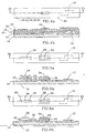
- FIGs. 1a-7a plane views
- 1b-7b corresponding cross-sectional views
- the sequence shows the formation of one TFR and one capacitor; however, in practice, the described method is likely to be employed to fabricate numerous TFRs and capacitors with a common set of process steps.
- an IC's active devices and at least one metal interconnect level are fabricated.
- a portion of a substrate 10 supports a metal interconnect 12, which is connected to one or more active devices (not shown).
- a dielectric layer 14 is deposited atop these existing structures. Layer 14 serves to protect the existing structures from the remaining process steps, as well as isolating the TFR and capacitor from the existing metal.
- the remaining layers required for the TFR and capacitor are deposited after the deposition of dielectric layer 14; this is shown in FIGs. 3a and 3b.
- a high resistivity film 16 from which the TFR will be made is deposited on layer 14, followed by a layer of metal 18 which will be used to form the bottom plate of the capacitor.
- the capacitor dielectric layer 20 is deposited next, with the thickness of the layer chosen to provide a particular capacitance value.
- Another metal layer 22 is deposited on the capacitor dielectric, which will be used to form the top plate of the capacitor.
- the desired TFR and capacitor structures are now formed.
- the top plate 24 of the capacitor is patterned and etched.
- the masking layer is then removed.
- the bottom plate 26 and TFR body 28 are patterned and etched, with those portions of thin film layer 16, metal layer 18, and dielectric layer 20 removed from areas which will not define resistors or capacitors.
- the capacitor's bottom plate stack can be etched with almost any combination of wet and dry etches.
- the active opening 30 which defines the TFR's length is patterned and etched. This removes the capacitor dielectric 20 and bottom plate metal 18 from above the area of the TFR body 28, except for "endcaps" 32 which are left at the TFR ends.
- FIGs. 7a and 7b The completion of the process is shown in FIGs. 7a and 7b.
- An inter-metal dielectric layer 34 is deposited over the TFR (36) and capacitor (38) structures, vias 40 are formed to provide contacts to the TFR and capacitor, and a metal layer 42 is deposited, patterned and etched to interconnect the TFR and capacitor to the other IC circuitry.
- Substrate 10 is typically silicon, and the IC's transistors and a metallization level are completed using well-known processes prior to commencing the present method.
- Dielectric layer 14 is preferably plasma-enhanced chemical vapor deposition (PECVD) oxide, having a thickness of 1000-6000 ⁇ .
- the thin film material 16 is preferably silicon-chromium-carbon (Si x Cr y C z ) having a sheet resistance of 50 - 3000 ohms/square, which is sputter deposited and optionally annealed.
- Bottom plate metal 18 is preferably titanium-tungsten (TiW) having a thickness of 500-3000 ⁇ , which is sputter deposited after an appropriate surface cleaning procedure. The bottom plate material should be chosen so as not to react with either the thin film material 16 or the capacitor dielectric layer 20.
- Capacitor dielectric layer 20 is preferably PECVD oxide having a thickness of 200-1500 ⁇ . Good control of this thickness is critical to achieving a desired capacitance value.
- dielectric layer 20 is oxide, the resulting capacitor is referred to as a metal-oxide-metal capacitor (MOMCAP).
- Top plate metal 22 preferably comprises a composite stack of TiW and an aluminum-copper (Al-Cu) alloy.
- the TiW is preferably sputter deposited to a thickness of 500-3000 ⁇
- the Al-Cu alloy is preferably sputtered - in a high-vacuum system without being exposed to the atmosphere - to a thickness of 1000-7000 ⁇ .
- the use of this composite stack gives the top plate a low resistivity, as well as providing symmetry to the capacitor.
- top plate 24 is patterned using standard photolithographic techniques. Due to the sensitivity of the capacitor to the loss of dielectric material around the active top plate area, top plate metal 22 is preferably wet etched in a 2 step process. Wet etching is preferred due its higher selectivity with respect to the capacitor's dielectric layer. Wet etching is enabled because 1) the (preferred) top plate metal is the TiW and Al-Cu alloy stack, and 2)because the capacitor's top plate is separate from the metal interconnects under dielectric layer 14, such that no fine features need to be maintained. When the top plate etch is complete, the photoresist is removed using standard dry resist strip processing.
- the bottom plate masking layer preferably fully encloses the top plate pattern.
- the bottom plate and TFR body are preferably etched using a multi-step etch process in a single dry etch tool, which should provide an excellent pattern transfer.
- the capacitor dielectric can first be etched in a standard CF 4 /CHF 3 plasma, the bottom plate's TiW etched in hot H 2 O 2 , and the thin film dry etched in either a standard Cl 2 and O 2 chemistry or a standard SF 6 chemistry. The photo pattern is then removed using standard dry resist strip processing.
- the etching of the TFR's active opening preferably comprises dry etching dielectric layer 20 using standard CF 4 /CHF 3 plasma, and etching metal layer 16 using hot H 2 O 2 . Note that since only the length of the resistor is defined in this step, this last mask is noc sensitive co misalignment in either the length or width dimensions of the TFR.
- the photoresist is preferably removed using a wet chemical stripper, since the thin film material can be sensitive to exposure to dry stripping processes.
- Intermetal dielectric layer 34 is preferably PECVD oxide, planarized using either a spin-on glass etch back step or with chemical-mechanical polishing (CMP).
- CMP chemical-mechanical polishing
- the vias are patterned and etched down to stop on three different levels: the capacitor top plate, the capacitor bottom plate and the TFR end caps, and the metal level found below dielectric layer 14.
- the present process does not preclude the use of an alternative metal process, such as using copper as the interconnect metal, or using dual-damascene metal patterning.
- top and bottom plates can comprise any metals capable of being wet-etched.
- FIGs. 8a-12a plane views
- FIGs. 8b-12b corresponding cross-sectional views
- the sequence starts as described above and as shown in FIGs. 1 and 2: a protective dielectric layer 14 is deposited over existing active devices and metallization 12 fabricated on a substrate 10. Then, as shown in FIGs. 8a and 8b, a layer of thin film material 50 is deposited over dielectric layer 14. In FIGs. 9a and 9b, thin film material 50 is patterned and etched to form the TFR body 52. This is followed by the deposition of the capacitor's bottom plate metal 54, dielectric layer 56, and top plate metal 58, as shown in FIGs. 10a and 10b.
- the capacitor top plate 60 is patterned and etched from metal layer 58, followed by the patterning and etching of the capacitor's bottom plate 62 and the TFR's active opening 64 as shown in FIGs. 12a and 12b, leaving TFR endcaps 66.
- the process is completed as described above and as shown in FIGs. 7a and 7b: an inuer-metal dielectric layer is deposited, vias are formed, and a metal interconnect layer is deposited, patterned, and etched to interconnect the TFR and capacitor to the other IC circuitry.
- the capacitor top plate can be wet-etched as described above, while the capacitor bottom plate can be patterned and etched using a standard CF 4 /CHF 3 plasma, with the bottom plate and TFR active opening etched in hot H 2 O 2 .
- This sequence can lead to higher precision resistor matching, since the very thin resistor material is patterned and etched separately.
- FIGs. 13a-16a plane views
- 13b-16b corresponding cross-sectional views
- the method begins as shown in FIGs. 1 and 2: with the deposition of a dielectric layer 14 over the active device and metallization structures already formed on substrate 10. As shown in FIGs. 13a and 13b, this is followed by the deposition of a thin film material layer 70, a bottom plate metal layer 72, and a capacitor dielectric layer 74.
- the bottom plate 76 of the capacitor and the body 78 of the TFR are patterned and etched next, followed by the patterning and etching of the TFR's active opening 80 and endcaps 82; the results of these steps are as shown in FIGs. 14a and 14b.
- the top plate metal layer 84 is deposited next, as shown in FIGs. 15a and 15b. Then, in FIGs. 16a and 16b, the capacitor's top plate 86 is patterned and etched. The process continues as shown in FIGs. 7a and 7b, with the formation of an inter-metal dielectric layer, vias, and a metal interconnect level.
- FIGs. 17a-20a plane views
- 17b-20b corresponding cross-sectional views
- the process begins in accordance with FIGs. 1, 2, 8 and 9: with a dielectric layer 14 deposited over existing active devices and metallization formed on a substrate 10, followed by the deposition of a thin film material layer 50 which is patterned and etched to form the body 52 of a TFR. As shown in FIGs. 17a and 17b, this is followed by depositing a first layer of metal 90 over the TFR body and dielectric layer 14, and depositing a second dielectric layer 92 over metal layer 90.
- the bottom plate 96 of the capacitor, the TFR's endcaps 98, and the TFR's active opening 100 are patterned and etched from layers 90 and 92.
- a layer of metal 102 is deposited in FIGs. 19a and 19b, from which the capacitor's top plate 104 is patterned and etched in FIGs. 20a and 20b.
- the process is completed in the same way as those described above: as shown in FIGs. 7a and 7b, with the formation of an inter-metal dielectric layer, vias, and a metal interconnect level.
Landscapes
- Semiconductor Integrated Circuits (AREA)
- Parts Printed On Printed Circuit Boards (AREA)
Claims (8)
- Procédé de fabrication d'une résistance à couche mince (TFR) et d'un condensateur sur un substrat commun de circuit intégré (IC), comprenant :le dépôt d'une première couche diélectrique (14) sur des structures existantes de composant actif et d'interconnexion métallique sur un substrat d'IC (10),le dépôt d'une couche de matériau pour couches minces (16) approprié pour former une TFR sur ladite première couche diélectrique,le dépôt d'une première couche de métal (18) sur ladite couche de matériau pour couches minces,le dépôt d'une deuxième couche diélectrique (20) sur ladite première couche de métal,le dépôt d'une deuxième couche de métal (22) sur ladite deuxième couche diélectrique,le dessin et la gravure chimique desdites première et deuxième couches de métal, de ladite deuxième couche diélectrique, et de ladite couche de matériau pour couches minces, pour former une TFR (36) ayant deux embouts (32) et un condensateur métal - diélectrique - métal (38) ayant des plaques inférieure et supérieure sur ledit substrat d'IC, ladite première couche de métal fournissant les embouts de ladite TFR et la plaque inférieure dudit condensateur,le dépôt d'une troisième couche diélectrique (34) sur ladite TFR et ledit condensateur,la gravure chimique des traversées (40) à travers ladite troisième couche diélectrique vers ladite TFR, ledit condensateur, et lesdites structures d'interconnexions métalliques, etle dépôt, le dessin et la gravure chimique d'une troisième couche de métal (42) pour fournir des interconnexions métalliques à ladite TFR, audit condensateur et auxdites structures d'interconnexions métalliques.
- Procédé selon la revendication 1, dans lequel ladite première couche diélectrique (14) comprend un oxyde déposé par dépôt chimique en phase vapeur assisté par plasma (PECVD).
- Procédé selon la revendication 1, dans lequel ledit matériau pour couches minces (16) est du silicium - chrome - carbone (SixCryCz).
- Procédé selon la revendication 1, dans lequel ladite première couche de métal (18) comprend du titane - tungstène (TiW).
- Procédé selon la revendication 1, dans lequel ladite deuxième couche diélectrique (20) comprend un oxyde déposé par dépôt chimique en phase vapeur assisté par plasma (PECVD).
- Procédé selon la revendication 1, dans lequel ladite deuxième couche de métal (22) comprend du titane - tungstène (TiW) et un alliage d'aluminium - cuivre.
- Procédé selon la revendication 1, dans lequel ladite étape de dessin et de gravure chimique comprend :le dessin de la plaque supérieure (24) dudit condensateur,la gravure chimique humide de ladite deuxième couche métallique (22) pour définir ladite plaque supérieure (24),le dessin de la plaque inférieure dudit condensateur et du corps de ladite TFR,la gravure chimique de ladite deuxième couche diélectrique, de ladite première couche métallique, et dudit matériau pour couches minces pour définir ladite plaque inférieure et le corps de ladite TFR,le dessin d'une ouverture active de ladite TFR, etla gravure chimique de ladite deuxième couche diélectrique (20) et de ladite première couche métallique (18) à partir de l'intérieur de ladite ouverture dessinée pour définir la longueur de ladite TFR.
- Procédé selon la revendication 7, dans lequel ledit condensateur (38) est un condensateur métal - oxyde - métal (MOMCAP) et ladite gravure chimique pour définir ladite plaque inférieure et le corps de ladite TFR, est exécutée avec un seul outil de gravure chimique à sec.
Applications Claiming Priority (2)
| Application Number | Priority Date | Filing Date | Title |
|---|---|---|---|
| US825386 | 2001-04-03 | ||
| US09/825,386 US6365480B1 (en) | 2000-11-27 | 2001-04-03 | IC resistor and capacitor fabrication method |
Publications (3)
| Publication Number | Publication Date |
|---|---|
| EP1248287A2 EP1248287A2 (fr) | 2002-10-09 |
| EP1248287A3 EP1248287A3 (fr) | 2004-11-10 |
| EP1248287B1 true EP1248287B1 (fr) | 2006-06-14 |
Family
ID=25243884
Family Applications (1)
| Application Number | Title | Priority Date | Filing Date |
|---|---|---|---|
| EP02252420A Expired - Lifetime EP1248287B1 (fr) | 2001-04-03 | 2002-04-03 | Procédé de fabrication d'une résistance et un condensateur dans un IC |
Country Status (3)
| Country | Link |
|---|---|
| US (1) | US6365480B1 (fr) |
| EP (1) | EP1248287B1 (fr) |
| DE (1) | DE60212238T2 (fr) |
Cited By (1)
| Publication number | Priority date | Publication date | Assignee | Title |
|---|---|---|---|---|
| US7898059B2 (en) | 2004-03-10 | 2011-03-01 | Freescale Semiconductor, Inc. | Semiconductor device comprising passive components |
Families Citing this family (36)
| Publication number | Priority date | Publication date | Assignee | Title |
|---|---|---|---|---|
| US7531417B2 (en) * | 1998-12-21 | 2009-05-12 | Megica Corporation | High performance system-on-chip passive device using post passivation process |
| US8421158B2 (en) * | 1998-12-21 | 2013-04-16 | Megica Corporation | Chip structure with a passive device and method for forming the same |
| US6303423B1 (en) * | 1998-12-21 | 2001-10-16 | Megic Corporation | Method for forming high performance system-on-chip using post passivation process |
| US8178435B2 (en) | 1998-12-21 | 2012-05-15 | Megica Corporation | High performance system-on-chip inductor using post passivation process |
| US6548389B2 (en) * | 2000-04-03 | 2003-04-15 | Matsushita Electric Industrial Co., Ltd. | Semiconductor device and method for fabricating the same |
| US6759275B1 (en) * | 2001-09-04 | 2004-07-06 | Megic Corporation | Method for making high-performance RF integrated circuits |
| US20030109125A1 (en) * | 2001-12-10 | 2003-06-12 | Chewnpu Jou | Fuse structure for a semiconductor device and manufacturing method thereof |
| US7022246B2 (en) * | 2003-01-06 | 2006-04-04 | International Business Machines Corporation | Method of fabrication of MIMCAP and resistor at same level |
| US7323751B2 (en) * | 2003-06-03 | 2008-01-29 | Texas Instruments Incorporated | Thin film resistor integration in a dual damascene structure |
| US6919244B1 (en) * | 2004-03-10 | 2005-07-19 | Motorola, Inc. | Method of making a semiconductor device, and semiconductor device made thereby |
| US7355282B2 (en) | 2004-09-09 | 2008-04-08 | Megica Corporation | Post passivation interconnection process and structures |
| US8008775B2 (en) | 2004-09-09 | 2011-08-30 | Megica Corporation | Post passivation interconnection structures |
| US8384189B2 (en) * | 2005-03-29 | 2013-02-26 | Megica Corporation | High performance system-on-chip using post passivation process |
| US7332403B1 (en) * | 2005-07-11 | 2008-02-19 | National Semiconductor Corporation | System and method for providing a buried thin film resistor having end caps defined by a dielectric mask |
| US7410879B1 (en) | 2005-07-11 | 2008-08-12 | National Semiconductor Corporation | System and method for providing a dual via architecture for thin film resistors |
| CN1901162B (zh) | 2005-07-22 | 2011-04-20 | 米辑电子股份有限公司 | 连续电镀制作线路组件的方法及线路组件结构 |
| US8124490B2 (en) * | 2006-12-21 | 2012-02-28 | Stats Chippac, Ltd. | Semiconductor device and method of forming passive devices |
| US7608538B2 (en) * | 2007-01-05 | 2009-10-27 | International Business Machines Corporation | Formation of vertical devices by electroplating |
| US9238870B2 (en) * | 2009-10-12 | 2016-01-19 | Texas Instruments Incorporated | Plasma etch for chromium alloys |
| US8426745B2 (en) * | 2009-11-30 | 2013-04-23 | Intersil Americas Inc. | Thin film resistor |
| DE102010008942B4 (de) * | 2010-02-23 | 2019-07-11 | Texas Instruments Deutschland Gmbh | Verfahren für eine vereinfachte Integration von hochgenauen Dünnfilmwiderständen |
| US8896408B2 (en) | 2013-03-14 | 2014-11-25 | Analog Devices, Inc. | Composite resistors |
| US10515949B2 (en) * | 2013-10-17 | 2019-12-24 | Taiwan Semiconductor Manufacturing Co., Ltd. | Integrated circuit and manufacturing method thereof |
| US9281355B2 (en) | 2014-05-05 | 2016-03-08 | Texas Instruments Deutschland Gmbh | Integrated thinfilm resistor and MIM capacitor with a low serial resistance |
| CN105226044B (zh) * | 2014-05-29 | 2018-12-18 | 联华电子股份有限公司 | 集成电路及形成集成电路的方法 |
| US10236123B2 (en) | 2015-07-19 | 2019-03-19 | Vq Research, Inc. | Methods and systems to minimize delamination of multilayer ceramic capacitors |
| US10332684B2 (en) | 2015-07-19 | 2019-06-25 | Vq Research, Inc. | Methods and systems for material cladding of multilayer ceramic capacitors |
| US10128047B2 (en) | 2015-07-19 | 2018-11-13 | Vq Research, Inc. | Methods and systems for increasing surface area of multilayer ceramic capacitors |
| US10431508B2 (en) | 2015-07-19 | 2019-10-01 | Vq Research, Inc. | Methods and systems to improve printed electrical components and for integration in circuits |
| US10242803B2 (en) | 2015-07-19 | 2019-03-26 | Vq Research, Inc. | Methods and systems for geometric optimization of multilayer ceramic capacitors |
| US10840322B2 (en) * | 2018-03-29 | 2020-11-17 | Texas Instruments Incorporated | Thin film resistor and top plate of capacitor sharing a layer |
| US10879172B2 (en) * | 2018-08-14 | 2020-12-29 | Taiwan Semiconductor Manufacturing Co., Ltd. | Semiconductor structure |
| JP7267786B2 (ja) * | 2019-03-13 | 2023-05-02 | エイブリック株式会社 | 半導体装置の製造方法 |
| US11637100B2 (en) | 2021-08-11 | 2023-04-25 | Globalfoundries Singapore Pte. Ltd. | Semiconductor device having capacitor and resistor and a method of forming the same |
| US12414359B2 (en) | 2021-09-15 | 2025-09-09 | Microchip Technology Incorporated | Integrated circuit structure including a metal-insulator-metal (MIM) capacitor module and a thin-film resistor (TFR) module |
| DE112022004397B4 (de) * | 2021-09-15 | 2026-02-12 | Microchip Technology Incorporated | Integrierte schaltungsstruktur, die ein metall-isolator-metall (mim) kondensatormodul und ein dünnschichtwiderstandsmodul (tfr) aufweist |
Family Cites Families (9)
| Publication number | Priority date | Publication date | Assignee | Title |
|---|---|---|---|---|
| DE2429434B2 (de) * | 1974-06-19 | 1979-10-04 | Siemens Ag, 1000 Berlin Und 8000 Muenchen | Verfahren zur Herstellung von Widerständen und Kondensatoren in Dunnschichtschaltungen |
| DE2506065C3 (de) * | 1975-02-13 | 1978-06-08 | Siemens Ag, 1000 Berlin Und 8000 Muenchen | Elektrische Dünnschichtschaltung |
| US3996551A (en) | 1975-10-20 | 1976-12-07 | The United States Of America As Represented By The Secretary Of The Navy | Chromium-silicon oxide thin film resistors |
| US4878770A (en) | 1987-09-09 | 1989-11-07 | Analog Devices, Inc. | IC chips with self-aligned thin film resistors |
| US4975386A (en) * | 1989-12-22 | 1990-12-04 | Micro Power Systems, Inc. | Process enhancement using molybdenum plugs in fabricating integrated circuits |
| US5479316A (en) | 1993-08-24 | 1995-12-26 | Analog Devices, Inc. | Integrated circuit metal-oxide-metal capacitor and method of making same |
| JPH0992512A (ja) * | 1995-09-25 | 1997-04-04 | Rohm Co Ltd | チップ型複合電子部品及びその製造方法 |
| US5926359A (en) | 1996-04-01 | 1999-07-20 | International Business Machines Corporation | Metal-insulator-metal capacitor |
| JP3028080B2 (ja) * | 1997-06-18 | 2000-04-04 | 日本電気株式会社 | 半導体装置の構造およびその製造方法 |
-
2001
- 2001-04-03 US US09/825,386 patent/US6365480B1/en not_active Expired - Lifetime
-
2002
- 2002-04-03 EP EP02252420A patent/EP1248287B1/fr not_active Expired - Lifetime
- 2002-04-03 DE DE60212238T patent/DE60212238T2/de not_active Expired - Lifetime
Cited By (1)
| Publication number | Priority date | Publication date | Assignee | Title |
|---|---|---|---|---|
| US7898059B2 (en) | 2004-03-10 | 2011-03-01 | Freescale Semiconductor, Inc. | Semiconductor device comprising passive components |
Also Published As
| Publication number | Publication date |
|---|---|
| US6365480B1 (en) | 2002-04-02 |
| DE60212238T2 (de) | 2007-03-29 |
| DE60212238D1 (de) | 2006-07-27 |
| EP1248287A3 (fr) | 2004-11-10 |
| EP1248287A2 (fr) | 2002-10-09 |
Similar Documents
| Publication | Publication Date | Title |
|---|---|---|
| US6365480B1 (en) | IC resistor and capacitor fabrication method | |
| US6426268B1 (en) | Thin film resistor fabrication method | |
| EP3140865B1 (fr) | Résistance à couche mince intégrée et condensateur mim | |
| US7960240B1 (en) | System and method for providing a dual via architecture for thin film resistors | |
| JP3371400B2 (ja) | 相互接続配線システムおよび形成方法 | |
| JP2004193602A (ja) | 銅による後工程(beol)技術用の金属−絶縁体−金属(mim)コンデンサ及び金属レジスタを製造する方法 | |
| US5918135A (en) | Methods for forming integrated circuit capacitors including dual electrode depositions | |
| US7808048B1 (en) | System and method for providing a buried thin film resistor having end caps defined by a dielectric mask | |
| WO2015103394A2 (fr) | Résistance à couche mince métallique et procédé associé | |
| US9679844B2 (en) | Manufacturing a damascene thin-film resistor | |
| US5985731A (en) | Method for forming a semiconductor device having a capacitor structure | |
| JP2004282081A (ja) | 二重ダマシン構造への薄膜レジスターの集積方法 | |
| US7169665B2 (en) | Capacitance process by using passivation film scheme | |
| US6943414B2 (en) | Method for fabricating a metal resistor in an IC chip and related structure | |
| US5913126A (en) | Methods of forming capacitors including expanded contact holes | |
| KR20040008432A (ko) | Mim 구조의 커패시터 제조방법 | |
| US7544580B2 (en) | Method for manufacturing passive components | |
| CN111033718A (zh) | 用于使用通孔阻滞层的薄膜电阻器的装置和方法 | |
| US7005343B2 (en) | Semiconductor device and method of manufacturing the same | |
| US20260129959A1 (en) | Thin film resistor and thin film metal-insulator-metal capacitor using sacrificial oxide for aluminum backend process | |
| US20260129881A1 (en) | Thin film resistor and thin film metal-insulator-metal capacitor in integrated circuit | |
| US6281092B1 (en) | Method for manufacturing a metal-to-metal capacitor utilizing only one masking step | |
| WO2026101747A1 (fr) | Résistance à film mince et condensateur métal-isolant-métal à film mince utilisant un oxyde sacrificiel pour un processus dorsal en aluminium | |
| CN117178360A (zh) | 包括金属-绝缘体-金属(mim)电容器模块和薄膜电阻器(tfr)模块的集成电路结构 | |
| JP2003188265A (ja) | Mim型容量素子の製造方法 |
Legal Events
| Date | Code | Title | Description |
|---|---|---|---|
| PUAI | Public reference made under article 153(3) epc to a published international application that has entered the european phase |
Free format text: ORIGINAL CODE: 0009012 |
|
| AK | Designated contracting states |
Kind code of ref document: A2 Designated state(s): AT BE CH CY DE DK ES FI FR GB GR IE IT LI LU MC NL PT SE TR |
|
| AX | Request for extension of the european patent |
Free format text: AL;LT;LV;MK;RO;SI |
|
| PUAL | Search report despatched |
Free format text: ORIGINAL CODE: 0009013 |
|
| AK | Designated contracting states |
Kind code of ref document: A3 Designated state(s): AT BE CH CY DE DK ES FI FR GB GR IE IT LI LU MC NL PT SE TR |
|
| AX | Request for extension of the european patent |
Extension state: AL LT LV MK RO SI |
|
| 17P | Request for examination filed |
Effective date: 20041230 |
|
| 17Q | First examination report despatched |
Effective date: 20050408 |
|
| AKX | Designation fees paid |
Designated state(s): DE FR GB |
|
| GRAP | Despatch of communication of intention to grant a patent |
Free format text: ORIGINAL CODE: EPIDOSNIGR1 |
|
| RIN1 | Information on inventor provided before grant (corrected) |
Inventor name: HUPPERT, GILBERT Inventor name: GLEASON, EDWARD Inventor name: DELAUS, MICHAEL, D. |
|
| GRAS | Grant fee paid |
Free format text: ORIGINAL CODE: EPIDOSNIGR3 |
|
| GRAA | (expected) grant |
Free format text: ORIGINAL CODE: 0009210 |
|
| AK | Designated contracting states |
Kind code of ref document: B1 Designated state(s): DE FR GB |
|
| REG | Reference to a national code |
Ref country code: GB Ref legal event code: FG4D |
|
| REF | Corresponds to: |
Ref document number: 60212238 Country of ref document: DE Date of ref document: 20060727 Kind code of ref document: P |
|
| ET | Fr: translation filed | ||
| PLBE | No opposition filed within time limit |
Free format text: ORIGINAL CODE: 0009261 |
|
| STAA | Information on the status of an ep patent application or granted ep patent |
Free format text: STATUS: NO OPPOSITION FILED WITHIN TIME LIMIT |
|
| 26N | No opposition filed |
Effective date: 20070315 |
|
| REG | Reference to a national code |
Ref country code: FR Ref legal event code: PLFP Year of fee payment: 15 |
|
| REG | Reference to a national code |
Ref country code: FR Ref legal event code: PLFP Year of fee payment: 16 |
|
| REG | Reference to a national code |
Ref country code: FR Ref legal event code: PLFP Year of fee payment: 17 |
|
| PGFP | Annual fee paid to national office [announced via postgrant information from national office to epo] |
Ref country code: FR Payment date: 20210323 Year of fee payment: 20 |
|
| PGFP | Annual fee paid to national office [announced via postgrant information from national office to epo] |
Ref country code: GB Payment date: 20210324 Year of fee payment: 20 |
|
| PGFP | Annual fee paid to national office [announced via postgrant information from national office to epo] |
Ref country code: DE Payment date: 20210323 Year of fee payment: 20 |
|
| REG | Reference to a national code |
Ref country code: DE Ref legal event code: R071 Ref document number: 60212238 Country of ref document: DE |
|
| REG | Reference to a national code |
Ref country code: GB Ref legal event code: PE20 Expiry date: 20220402 |
|
| PG25 | Lapsed in a contracting state [announced via postgrant information from national office to epo] |
Ref country code: GB Free format text: LAPSE BECAUSE OF EXPIRATION OF PROTECTION Effective date: 20220402 |