EP1248295A2 - Elément semi-conducteur, structure de connection, dispositif semi-conducteur utilisant plusieurs de ces éléments et procédés de fabrication - Google Patents
Elément semi-conducteur, structure de connection, dispositif semi-conducteur utilisant plusieurs de ces éléments et procédés de fabrication Download PDFInfo
- Publication number
- EP1248295A2 EP1248295A2 EP20020007769 EP02007769A EP1248295A2 EP 1248295 A2 EP1248295 A2 EP 1248295A2 EP 20020007769 EP20020007769 EP 20020007769 EP 02007769 A EP02007769 A EP 02007769A EP 1248295 A2 EP1248295 A2 EP 1248295A2
- Authority
- EP
- European Patent Office
- Prior art keywords
- conductive bump
- semiconductor element
- semiconductor
- conductive
- bump
- Prior art date
- Legal status (The legal status is an assumption and is not a legal conclusion. Google has not performed a legal analysis and makes no representation as to the accuracy of the status listed.)
- Withdrawn
Links
Images


Classifications
-
- H—ELECTRICITY
- H10—SEMICONDUCTOR DEVICES; ELECTRIC SOLID-STATE DEVICES NOT OTHERWISE PROVIDED FOR
- H10W—GENERIC PACKAGES, INTERCONNECTIONS, CONNECTORS OR OTHER CONSTRUCTIONAL DETAILS OF DEVICES COVERED BY CLASS H10
- H10W74/00—Encapsulations, e.g. protective coatings
- H10W74/01—Manufacture or treatment
- H10W74/012—Manufacture or treatment of encapsulations on active surfaces of flip-chip devices, e.g. forming underfills
-
- H—ELECTRICITY
- H10—SEMICONDUCTOR DEVICES; ELECTRIC SOLID-STATE DEVICES NOT OTHERWISE PROVIDED FOR
- H10W—GENERIC PACKAGES, INTERCONNECTIONS, CONNECTORS OR OTHER CONSTRUCTIONAL DETAILS OF DEVICES COVERED BY CLASS H10
- H10W20/00—Interconnections in chips, wafers or substrates
- H10W20/20—Interconnections within wafers or substrates, e.g. through-silicon vias [TSV]
-
- H—ELECTRICITY
- H10—SEMICONDUCTOR DEVICES; ELECTRIC SOLID-STATE DEVICES NOT OTHERWISE PROVIDED FOR
- H10W—GENERIC PACKAGES, INTERCONNECTIONS, CONNECTORS OR OTHER CONSTRUCTIONAL DETAILS OF DEVICES COVERED BY CLASS H10
- H10W74/00—Encapsulations, e.g. protective coatings
- H10W74/10—Encapsulations, e.g. protective coatings characterised by their shape or disposition
- H10W74/15—Encapsulations, e.g. protective coatings characterised by their shape or disposition on active surfaces of flip-chip devices, e.g. underfills
-
- H—ELECTRICITY
- H10—SEMICONDUCTOR DEVICES; ELECTRIC SOLID-STATE DEVICES NOT OTHERWISE PROVIDED FOR
- H10W—GENERIC PACKAGES, INTERCONNECTIONS, CONNECTORS OR OTHER CONSTRUCTIONAL DETAILS OF DEVICES COVERED BY CLASS H10
- H10W90/00—Package configurations
-
- H—ELECTRICITY
- H10—SEMICONDUCTOR DEVICES; ELECTRIC SOLID-STATE DEVICES NOT OTHERWISE PROVIDED FOR
- H10W—GENERIC PACKAGES, INTERCONNECTIONS, CONNECTORS OR OTHER CONSTRUCTIONAL DETAILS OF DEVICES COVERED BY CLASS H10
- H10W72/00—Interconnections or connectors in packages
- H10W72/20—Bump connectors, e.g. solder bumps or copper pillars; Dummy bumps; Thermal bumps
-
- H—ELECTRICITY
- H10—SEMICONDUCTOR DEVICES; ELECTRIC SOLID-STATE DEVICES NOT OTHERWISE PROVIDED FOR
- H10W—GENERIC PACKAGES, INTERCONNECTIONS, CONNECTORS OR OTHER CONSTRUCTIONAL DETAILS OF DEVICES COVERED BY CLASS H10
- H10W72/00—Interconnections or connectors in packages
- H10W72/851—Dispositions of multiple connectors or interconnections
- H10W72/853—On the same surface
- H10W72/856—Bump connectors and die-attach connectors
-
- H—ELECTRICITY
- H10—SEMICONDUCTOR DEVICES; ELECTRIC SOLID-STATE DEVICES NOT OTHERWISE PROVIDED FOR
- H10W—GENERIC PACKAGES, INTERCONNECTIONS, CONNECTORS OR OTHER CONSTRUCTIONAL DETAILS OF DEVICES COVERED BY CLASS H10
- H10W72/00—Interconnections or connectors in packages
- H10W72/90—Bond pads, in general
- H10W72/941—Dispositions of bond pads
- H10W72/9415—Dispositions of bond pads relative to the surface, e.g. recessed, protruding
-
- H—ELECTRICITY
- H10—SEMICONDUCTOR DEVICES; ELECTRIC SOLID-STATE DEVICES NOT OTHERWISE PROVIDED FOR
- H10W—GENERIC PACKAGES, INTERCONNECTIONS, CONNECTORS OR OTHER CONSTRUCTIONAL DETAILS OF DEVICES COVERED BY CLASS H10
- H10W90/00—Package configurations
- H10W90/20—Configurations of stacked chips
- H10W90/297—Configurations of stacked chips characterised by the through-semiconductor vias [TSVs] in the stacked chips
-
- H—ELECTRICITY
- H10—SEMICONDUCTOR DEVICES; ELECTRIC SOLID-STATE DEVICES NOT OTHERWISE PROVIDED FOR
- H10W—GENERIC PACKAGES, INTERCONNECTIONS, CONNECTORS OR OTHER CONSTRUCTIONAL DETAILS OF DEVICES COVERED BY CLASS H10
- H10W90/00—Package configurations
- H10W90/701—Package configurations characterised by the relative positions of pads or connectors relative to package parts
- H10W90/721—Package configurations characterised by the relative positions of pads or connectors relative to package parts of bump connectors
- H10W90/722—Package configurations characterised by the relative positions of pads or connectors relative to package parts of bump connectors between stacked chips
-
- H—ELECTRICITY
- H10—SEMICONDUCTOR DEVICES; ELECTRIC SOLID-STATE DEVICES NOT OTHERWISE PROVIDED FOR
- H10W—GENERIC PACKAGES, INTERCONNECTIONS, CONNECTORS OR OTHER CONSTRUCTIONAL DETAILS OF DEVICES COVERED BY CLASS H10
- H10W90/00—Package configurations
- H10W90/701—Package configurations characterised by the relative positions of pads or connectors relative to package parts
- H10W90/721—Package configurations characterised by the relative positions of pads or connectors relative to package parts of bump connectors
- H10W90/724—Package configurations characterised by the relative positions of pads or connectors relative to package parts of bump connectors between a chip and a stacked insulating package substrate, interposer or RDL
-
- H—ELECTRICITY
- H10—SEMICONDUCTOR DEVICES; ELECTRIC SOLID-STATE DEVICES NOT OTHERWISE PROVIDED FOR
- H10W—GENERIC PACKAGES, INTERCONNECTIONS, CONNECTORS OR OTHER CONSTRUCTIONAL DETAILS OF DEVICES COVERED BY CLASS H10
- H10W90/00—Package configurations
- H10W90/701—Package configurations characterised by the relative positions of pads or connectors relative to package parts
- H10W90/731—Package configurations characterised by the relative positions of pads or connectors relative to package parts of die-attach connectors
- H10W90/732—Package configurations characterised by the relative positions of pads or connectors relative to package parts of die-attach connectors between stacked chips
-
- H—ELECTRICITY
- H10—SEMICONDUCTOR DEVICES; ELECTRIC SOLID-STATE DEVICES NOT OTHERWISE PROVIDED FOR
- H10W—GENERIC PACKAGES, INTERCONNECTIONS, CONNECTORS OR OTHER CONSTRUCTIONAL DETAILS OF DEVICES COVERED BY CLASS H10
- H10W90/00—Package configurations
- H10W90/701—Package configurations characterised by the relative positions of pads or connectors relative to package parts
- H10W90/731—Package configurations characterised by the relative positions of pads or connectors relative to package parts of die-attach connectors
- H10W90/734—Package configurations characterised by the relative positions of pads or connectors relative to package parts of die-attach connectors between a chip and a stacked insulating package substrate, interposer or RDL
Definitions
- the present invention relates to a structure of a semiconductor element, a connection structure thereof and a semiconductor device formed by stacking such semiconductor elements.
- the present invention also relates to processes for making such semiconductor element and devices.
- TCP a tape carrier package
- a large capacity semiconductor device has been contemplated by stacking such semiconductor elements represented by TCP.
- the semiconductor device since the semiconductor device should be small and thin, a connection structure is required which is capable of stacking as many as possible of the semiconductor elements in a predetermined height.
- Fig. 1 shows a conventional connection structure for a prior art stacking type semiconductor device.
- a semiconductor element 1 has Al pads 3 on a circuitry surface 2. On each of the Al pad, an Au bump 4 is formed for the electric connection with other semiconductor element 1'.
- This semiconductor element is integral with an interposer 9 consisting of a circuit layer 6, an insulation layer 7 and solder bumps 8 via an underfil layer 5 made of a resin (such as epoxy resin) to complete a stacking semiconductor device. Since this stacking semiconductor device is of a structure for connecting the Au bump 4 of the semiconductor element 1 with the circuit layer 6 of the interposer, the solder bump 8 becomes a connection terminal for the connection with another stacking semiconductor device.
- the semiconductor element l'of the other stacking semiconductor device is accommodated in a lower space of the interposer in the stacking semiconductor device, and the solder bumps 8 are in contact with the circuit layer of the other stacking semiconductor device.
- the respective semiconductor element is mounted onto the interposer to form one package, which is then stacked on the other to provide a large-capacity stacked type semiconductor device while ensuring the electric connection between the respective semiconductor elements.
- the interposer is used for stacking the semiconductor elements, a high-speed response becomes difficult and this limits the use of the semiconductor device.
- the stacking type semiconductor device is required to have a stack structure and/or a connection structure capable of realizing not only a large capacity, a small size and a small thickness but also a high-speed response.
- the present invention has been made in view of the above-mentioned requirements.
- an object of the present invention is to provide a semiconductor element involving an excellent stacking structure and/or a connection structure for semiconductor elements capable of realizing a large capacity, a small size and a small thickness as well as a high- speed response, and also a semiconductor device formed by stacking such semiconductor elements.
- the inventor of the present invention initially studied the prior art connection structure shown in Fig. 1 when solving the above-mentioned problems. As a result, it was noted that, if the interposer is eliminated from the prior art connection structure, it is possible to stack more semiconductor elements if the same height of the connection structure is to be maintained, or to further reduce the thickness of the semiconductor device if the same capacity of the semiconductor device is to be maintained, in addition to which, it is possible to respond to a high-speed operation so far as the interposer is eliminated. Based on this idea, the inventor diligently studied to obtain a connection structure capable of electrically interconnecting the semiconductor elements stacked to form a plurality of layers without using an interposer.
- a semiconductor element comprising: an element body having a first surface and a second, opposite surface; a conductive bump formed on the first surface of the element body; and the element body having a via hole penetrating from the conductive bump on the first surface to the second surface.
- An inner wall of the via hole is coated with an insulating layer and a conductive film, so that the conductive film is electrically connected to the conductive bump.
- the material of the conductive film is Au or Cu.
- the material of the insulating layer is SiO 2 .
- connection structure comprising: a first semiconductor element having a first conductive bump; a second semiconductor element comprising: an element body having a first surface and a second, opposite surface; a second conductive bump formed on the first surface of the element body; and the element body having a via hole penetrating from the conductive bump on the first surface to the second surface; and the first and second semiconductor elements are mutually arranged in such a manner that the first conductive bump is in contact with the second surface of the second semiconductor element at a position of the vial hole; and means for electrically connecting the first conductive bump with the second conductive bump.
- a semiconductor device comprising a plurality of semiconductor elements stacked on one another, including at least:
- a process for manufacturing a semiconductor element comprising the following steps of: forming a conductive bump on a first surface of a semiconductor element body; and forming a via hole which penetrates the element body from the conductive bump on the first surface to a second, opposite surface of the element body.
- the process further comprises the following steps of: coating an inner wall of the via hole with an insulating layer and a conductive film, so that the conductive bump is electrically connected to the conductive film.
- a process for manufacturing a semiconductor device comprising a plurality of semiconductor elements stacked on one another, the process comprising the following steps of:
- Fig. 2 shows one embodiment of a semiconductor element according to the present invention.
- via-holes 10 are formed, each of which passes through a circuitry surface 2 and reaches a back surface of an Au bump (conductive bump) 4 formed on an Al pad 3.
- Au bump conductive bump
- a conductive cover film 12 is formed on the inner surface of the via-hole 10 via an insulation layer 11.
- the conductive cover film 12 is preferably made of Au or Cu, another conductive metal or alloy may be used.
- the insulation layer 11 is preferably made of SiO 2 because the insulation layer and the conductive cover film can be easily formed and the insulation layer can be brought into tight contact with the conductive cover film and a wafer, another insulation material may be used provided it satisfies such requirements.
- the insulation cover film 12 is continuous with the conductive bump, it functions as a connection terminal when one semiconductor element is electrically connected to another semiconductor element.
- FIG. 4 One embodiment in which two semiconductor elements are stacked is illustrated in Fig. 4. As shown in Fig. 4, since a conductive bump 4 of the one semiconductor elements (the upper one in the drawing) abuts a via-hole 10 of the other semiconductor element (the lower one in the drawing) and is in contact with the conductive cover film 12, the conductive bumps 4 of the upper and lower conductive bumps 4 are connected to each other through the conductive cover film 12, whereby the electrical connection is directly made between the upper and lower semiconductor elements.
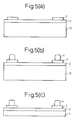
- an Al pad 3 is provided in the conventional manner (see Fig. 5(a)), and then an Au bump 4 (which is a conductive bump of about 35 ⁇ m high) is formed by using a plating or a bump bonder (see Fig. 5(b)). Thereafter, a back surface of the wafer 13 is abraded to have a desired thickness (for example, an original thickness of about 650 ⁇ m is abraded to about 50 ⁇ m). Thus the semiconductor element is completed.
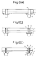
- a laser beam for example, an ultraviolet laser beam
- a laser beam of a predetermined intensity is irradiated from above the semiconductor element 1 to a position corresponding to the Au bump to form a via-hole 10 of a proper size (for example, having a diameter of 10 ⁇ m or less) passing through the semiconductor element to reach the back surface of the Au bump 4 (see Fig. 6(a)).
- the Au bump 4 serves as a stopper for precisely controlling the boring process carried out by the laser beam.
- an insulation layer 11 is formed on the inner surface of the via-hole 10 by using CVD or a spin coater (see Fig. 6(b)).
- CVD tetraethoxysilane is vaporized to form an insulation layer of SiO 2 .
- a conductive cover film 12 is formed on the surface of the insulation layer 11.
- a thin semiconductor element according to the present invention is produced, which is suitably used for preparing a stacking type semiconductor device.
- Fig. 7 illustrates one embodiment of a semiconductor device constituted by stacking the semiconductor elements according to the present invention on a circuit board 14 having solder bumps 8.
- the semiconductor elements are electrically connected to each other by the connection structure according to the present invention.
- the semiconductor elements having the same dimension and structure are sequentially stacked to establish a direct electric connection between them, it is possible to obtain a semiconductor device large in capacity, small in size and thickness as well as responsive to a high-speed operation.
- the semiconductor elements having the same dimension and structure are sequentially stacked, even if the semiconductor element is heated, the thermal expansion of the respective semiconductor elements becomes approximately equal, whereby the electric connection between the semiconductor elements can be always maintained in a stable state.
Landscapes
- Internal Circuitry In Semiconductor Integrated Circuit Devices (AREA)
- Wire Bonding (AREA)
Applications Claiming Priority (2)
| Application Number | Priority Date | Filing Date | Title |
|---|---|---|---|
| JP2001109118A JP2002305282A (ja) | 2001-04-06 | 2001-04-06 | 半導体素子とその接続構造及び半導体素子を積層した半導体装置 |
| JP2001109118 | 2001-04-06 |
Publications (2)
| Publication Number | Publication Date |
|---|---|
| EP1248295A2 true EP1248295A2 (fr) | 2002-10-09 |
| EP1248295A3 EP1248295A3 (fr) | 2005-07-13 |
Family
ID=18961123
Family Applications (1)
| Application Number | Title | Priority Date | Filing Date |
|---|---|---|---|
| EP02007769A Withdrawn EP1248295A3 (fr) | 2001-04-06 | 2002-04-05 | Elément semi-conducteur, structure de connection, dispositif semi-conducteur utilisant plusieurs de ces éléments et procédés de fabrication |
Country Status (3)
| Country | Link |
|---|---|
| US (1) | US20020145191A1 (fr) |
| EP (1) | EP1248295A3 (fr) |
| JP (1) | JP2002305282A (fr) |
Cited By (5)
| Publication number | Priority date | Publication date | Assignee | Title |
|---|---|---|---|---|
| EP1418617A3 (fr) * | 2002-11-05 | 2004-05-26 | Shinko Electric Co. Ltd. | Composant semiconducteur et méthode de fabrication correspondante |
| EP1427006A1 (fr) * | 2002-12-03 | 2004-06-09 | Shinko Electric Industries Co., Ltd. | Structure d'encapsulation pour éléments électroniques et méthode pour sa fabrication |
| WO2004038798A3 (fr) * | 2002-10-22 | 2004-07-29 | Unitive Int Ltd | Structures electroniques empilees comprenant des substrats decales |
| EP1777742A3 (fr) * | 2005-10-18 | 2008-08-20 | Shinko Electric Industries Co., Ltd. | Puce à semi-conducteur avec trou d'interconnexion traversant et procédé de fabrication de la puce à semi-conducteur |
| US8674494B2 (en) | 2011-08-31 | 2014-03-18 | Samsung Electronics Co., Ltd. | Semiconductor package having supporting plate and method of forming the same |
Families Citing this family (16)
| Publication number | Priority date | Publication date | Assignee | Title |
|---|---|---|---|---|
| JP3646719B2 (ja) * | 2003-06-19 | 2005-05-11 | セイコーエプソン株式会社 | 半導体装置及びその製造方法、回路基板並びに電子機器 |
| JP4340517B2 (ja) | 2003-10-30 | 2009-10-07 | Okiセミコンダクタ株式会社 | 半導体装置及びその製造方法 |
| WO2005093834A1 (fr) * | 2004-03-25 | 2005-10-06 | Nec Corporation | Dispositif semi-conducteur à empilement de puces |
| JP4577687B2 (ja) * | 2005-03-17 | 2010-11-10 | エルピーダメモリ株式会社 | 半導体装置 |
| JP2007067082A (ja) * | 2005-08-30 | 2007-03-15 | Disco Abrasive Syst Ltd | ウエーハの穿孔方法 |
| US7906846B2 (en) | 2005-09-06 | 2011-03-15 | Nec Corporation | Semiconductor device for implementing signal transmission and/or power supply by means of the induction of a coil |
| JP2007305955A (ja) * | 2006-04-10 | 2007-11-22 | Toshiba Corp | 半導体装置及びその製造方法 |
| JP2008068292A (ja) * | 2006-09-14 | 2008-03-27 | Disco Abrasive Syst Ltd | ビアホールの加工方法 |
| JP4773307B2 (ja) | 2006-09-15 | 2011-09-14 | Okiセミコンダクタ株式会社 | 半導体装置の製造方法 |
| JP2008073711A (ja) * | 2006-09-20 | 2008-04-03 | Disco Abrasive Syst Ltd | ビアホールの加工方法 |
| JP2008073740A (ja) * | 2006-09-22 | 2008-04-03 | Disco Abrasive Syst Ltd | ビアホールの加工方法 |
| JP2008155274A (ja) * | 2006-12-26 | 2008-07-10 | Disco Abrasive Syst Ltd | ウエーハの加工方法 |
| JP2008212999A (ja) * | 2007-03-06 | 2008-09-18 | Disco Abrasive Syst Ltd | レーザー加工装置 |
| JP4939452B2 (ja) * | 2008-02-07 | 2012-05-23 | ラピスセミコンダクタ株式会社 | 半導体装置の製造方法 |
| US8390130B1 (en) * | 2011-01-06 | 2013-03-05 | Amkor Technology, Inc. | Through via recessed reveal structure and method |
| KR101918609B1 (ko) | 2012-01-11 | 2018-11-14 | 삼성전자 주식회사 | 집적회로 소자 |
Citations (1)
| Publication number | Priority date | Publication date | Assignee | Title |
|---|---|---|---|---|
| EP1061578A1 (fr) * | 1998-12-16 | 2000-12-20 | Seiko Epson Corporation | Puce de semi-conducteur, dispositif a semi-conducteur, carte de circuits et materiel electronique et leurs procedes de production |
Family Cites Families (7)
| Publication number | Priority date | Publication date | Assignee | Title |
|---|---|---|---|---|
| GB9018766D0 (en) * | 1990-08-28 | 1990-10-10 | Lsi Logic Europ | Stacking of integrated circuits |
| US5229647A (en) * | 1991-03-27 | 1993-07-20 | Micron Technology, Inc. | High density data storage using stacked wafers |
| JP2622038B2 (ja) * | 1991-06-03 | 1997-06-18 | シャープ株式会社 | 半導体装置及びその製造方法 |
| WO1996013062A1 (fr) * | 1994-10-19 | 1996-05-02 | Ceram Incorporated | Dispositif et procede de fabrication d'empilements de series de plaquettes |
| JP3186941B2 (ja) * | 1995-02-07 | 2001-07-11 | シャープ株式会社 | 半導体チップおよびマルチチップ半導体モジュール |
| US6222276B1 (en) * | 1998-04-07 | 2001-04-24 | International Business Machines Corporation | Through-chip conductors for low inductance chip-to-chip integration and off-chip connections |
| US6122187A (en) * | 1998-11-23 | 2000-09-19 | Micron Technology, Inc. | Stacked integrated circuits |
-
2001
- 2001-04-06 JP JP2001109118A patent/JP2002305282A/ja active Pending
-
2002
- 2002-04-02 US US10/114,518 patent/US20020145191A1/en not_active Abandoned
- 2002-04-05 EP EP02007769A patent/EP1248295A3/fr not_active Withdrawn
Patent Citations (1)
| Publication number | Priority date | Publication date | Assignee | Title |
|---|---|---|---|---|
| EP1061578A1 (fr) * | 1998-12-16 | 2000-12-20 | Seiko Epson Corporation | Puce de semi-conducteur, dispositif a semi-conducteur, carte de circuits et materiel electronique et leurs procedes de production |
Cited By (14)
| Publication number | Priority date | Publication date | Assignee | Title |
|---|---|---|---|---|
| WO2004038798A3 (fr) * | 2002-10-22 | 2004-07-29 | Unitive Int Ltd | Structures electroniques empilees comprenant des substrats decales |
| US7495326B2 (en) | 2002-10-22 | 2009-02-24 | Unitive International Limited | Stacked electronic structures including offset substrates |
| US7507602B2 (en) | 2002-11-05 | 2009-03-24 | Shinko Electric Industries Co., Ltd. | Semiconductor device and method of manufacturing the same |
| US6958544B2 (en) | 2002-11-05 | 2005-10-25 | Shinko Electric Industries Co., Ltd. | Semiconductor device and method of manufacturing the same |
| EP1801866A3 (fr) * | 2002-11-05 | 2007-12-19 | Shinko Electric Industries Co., Ltd. | Composant semiconducteur et méthode de fabrication correspondante |
| EP1418617A3 (fr) * | 2002-11-05 | 2004-05-26 | Shinko Electric Co. Ltd. | Composant semiconducteur et méthode de fabrication correspondante |
| US6943442B2 (en) | 2002-12-03 | 2005-09-13 | Shinko Electric Industries Co., Ltd. | Electronic parts packaging structure having mutually connected electronic parts that are buried in a insulating film |
| US7084009B2 (en) | 2002-12-03 | 2006-08-01 | Shinko Electric Industries Co., Ltd. | Method of manufacturing a packaging structure for electronic parts buried in an insulating film formed on the electronic parts and a wiring substrate |
| EP1427006A1 (fr) * | 2002-12-03 | 2004-06-09 | Shinko Electric Industries Co., Ltd. | Structure d'encapsulation pour éléments électroniques et méthode pour sa fabrication |
| EP1777742A3 (fr) * | 2005-10-18 | 2008-08-20 | Shinko Electric Industries Co., Ltd. | Puce à semi-conducteur avec trou d'interconnexion traversant et procédé de fabrication de la puce à semi-conducteur |
| US7576004B2 (en) | 2005-10-18 | 2009-08-18 | Shinko Electric Industries Co., Ltd. | Semiconductor chip and method of manufacturing semiconductor chip |
| US7592700B2 (en) | 2005-10-18 | 2009-09-22 | Shinko Electric Industries Co., Ltd. | Semiconductor chip and method of manufacturing semiconductor chip |
| US8674494B2 (en) | 2011-08-31 | 2014-03-18 | Samsung Electronics Co., Ltd. | Semiconductor package having supporting plate and method of forming the same |
| US9412720B2 (en) | 2011-08-31 | 2016-08-09 | Samsung Electronics Co., Ltd. | Semiconductor package having supporting plate and method of forming the same |
Also Published As
| Publication number | Publication date |
|---|---|
| US20020145191A1 (en) | 2002-10-10 |
| JP2002305282A (ja) | 2002-10-18 |
| EP1248295A3 (fr) | 2005-07-13 |
Similar Documents
| Publication | Publication Date | Title |
|---|---|---|
| EP1248295A2 (fr) | Elément semi-conducteur, structure de connection, dispositif semi-conducteur utilisant plusieurs de ces éléments et procédés de fabrication | |
| US6022758A (en) | Process for manufacturing solder leads on a semiconductor device package | |
| US7531890B2 (en) | Multi-chip package (MCP) with a conductive bar and method for manufacturing the same | |
| JP2819284B2 (ja) | 半導体パッケージ用基板およびその製造方法と その基板を利用した積層型半導体パッケージ | |
| EP0208494B1 (fr) | Procédé pour fabriquer un appareil semi-conducteur comprenant deux dispositifs semi-conducteurs | |
| US6800505B2 (en) | Semiconductor device including edge bond pads and related methods | |
| US6413798B2 (en) | Package having very thin semiconductor chip, multichip module assembled by the package, and method for manufacturing the same | |
| KR100282285B1 (ko) | 적층된 다중칩 모듈 및 그의 제조방법 | |
| US5838061A (en) | Semiconductor package including a semiconductor chip adhesively bonded thereto | |
| US6469260B2 (en) | Wiring boards, semiconductor devices and their production processes | |
| JP2017038075A (ja) | エリアアレイユニットコネクタを備えるスタック可能モールド超小型電子パッケージ | |
| JP2005327984A (ja) | 電子部品及び電子部品実装構造の製造方法 | |
| US20040135243A1 (en) | Semiconductor device, its manufacturing method and electronic device | |
| US20030122253A1 (en) | Wafer levelpackaging and chip structure | |
| JP2003163324A (ja) | ユニット半導体装置及びその製造方法並びに3次元積層型半導体装置 | |
| US20020070446A1 (en) | Semiconductor device and method for the production thereof | |
| US5863812A (en) | Process for manufacturing a multi layer bumped semiconductor device | |
| TW550768B (en) | Flip-chip on film assembly for ball grid array packages | |
| US7706148B2 (en) | Stack structure of circuit boards embedded with semiconductor chips | |
| US20020093093A1 (en) | Semiconductor package with stacked dies | |
| US20090045444A1 (en) | Integrated device and circuit system | |
| JP2004146728A (ja) | 半導体装置とその製造方法 | |
| JPH09270490A (ja) | 接続部構造および接続方法並びに半導体装置およびその製造方法 | |
| US20240120299A1 (en) | Semiconductor package | |
| JP2005101186A (ja) | 積層型半導体集積回路 |
Legal Events
| Date | Code | Title | Description |
|---|---|---|---|
| PUAI | Public reference made under article 153(3) epc to a published international application that has entered the european phase |
Free format text: ORIGINAL CODE: 0009012 |
|
| 17P | Request for examination filed |
Effective date: 20020405 |
|
| AK | Designated contracting states |
Kind code of ref document: A2 Designated state(s): AT BE CH CY DE DK ES FI FR GB GR IE IT LI LU MC NL PT SE TR |
|
| AX | Request for extension of the european patent |
Free format text: AL;LT;LV;MK;RO;SI |
|
| PUAL | Search report despatched |
Free format text: ORIGINAL CODE: 0009013 |
|
| AK | Designated contracting states |
Kind code of ref document: A3 Designated state(s): AT BE CH CY DE DK ES FI FR GB GR IE IT LI LU MC NL PT SE TR |
|
| AX | Request for extension of the european patent |
Extension state: AL LT LV MK RO SI |
|
| AKX | Designation fees paid |
Designated state(s): CH DE LI |
|
| STAA | Information on the status of an ep patent application or granted ep patent |
Free format text: STATUS: THE APPLICATION IS DEEMED TO BE WITHDRAWN |
|
| 18D | Application deemed to be withdrawn |
Effective date: 20100427 |