EP1251402A1 - Lithographisher Apparat - Google Patents
Lithographisher Apparat Download PDFInfo
- Publication number
- EP1251402A1 EP1251402A1 EP02252340A EP02252340A EP1251402A1 EP 1251402 A1 EP1251402 A1 EP 1251402A1 EP 02252340 A EP02252340 A EP 02252340A EP 02252340 A EP02252340 A EP 02252340A EP 1251402 A1 EP1251402 A1 EP 1251402A1
- Authority
- EP
- European Patent Office
- Prior art keywords
- pattern
- projection system
- aberration
- radiation
- compensation
- Prior art date
- Legal status (The legal status is an assumption and is not a legal conclusion. Google has not performed a legal analysis and makes no representation as to the accuracy of the status listed.)
- Granted
Links
- 230000004075 alteration Effects 0.000 claims abstract description 79
- 238000006073 displacement reaction Methods 0.000 claims abstract description 28
- 238000004519 manufacturing process Methods 0.000 claims abstract description 26
- 230000035945 sensitivity Effects 0.000 claims abstract description 20
- 238000009826 distribution Methods 0.000 claims abstract description 12
- 238000004364 calculation method Methods 0.000 claims abstract description 9
- 230000005855 radiation Effects 0.000 claims description 65
- 239000000758 substrate Substances 0.000 claims description 54
- 238000000059 patterning Methods 0.000 claims description 37
- 230000008859 change Effects 0.000 claims description 21
- 238000000034 method Methods 0.000 claims description 20
- 230000010363 phase shift Effects 0.000 claims description 19
- 238000005286 illumination Methods 0.000 claims description 15
- 230000003287 optical effect Effects 0.000 claims description 9
- 239000000463 material Substances 0.000 claims description 8
- 238000013519 translation Methods 0.000 claims description 8
- 230000008569 process Effects 0.000 claims description 6
- 230000000694 effects Effects 0.000 abstract description 7
- 230000007423 decrease Effects 0.000 abstract description 4
- 230000006870 function Effects 0.000 description 26
- 239000010410 layer Substances 0.000 description 16
- 238000003384 imaging method Methods 0.000 description 14
- 230000014509 gene expression Effects 0.000 description 5
- 238000005457 optimization Methods 0.000 description 5
- 238000001459 lithography Methods 0.000 description 4
- 238000012545 processing Methods 0.000 description 4
- 238000011065 in-situ storage Methods 0.000 description 3
- XUIMIQQOPSSXEZ-UHFFFAOYSA-N Silicon Chemical compound [Si] XUIMIQQOPSSXEZ-UHFFFAOYSA-N 0.000 description 2
- 238000003491 array Methods 0.000 description 2
- 230000001419 dependent effect Effects 0.000 description 2
- 238000013461 design Methods 0.000 description 2
- 230000001627 detrimental effect Effects 0.000 description 2
- 239000011159 matrix material Substances 0.000 description 2
- 238000005259 measurement Methods 0.000 description 2
- 229910052710 silicon Inorganic materials 0.000 description 2
- 239000010703 silicon Substances 0.000 description 2
- 238000012360 testing method Methods 0.000 description 2
- 101000634119 Arabidopsis thaliana RNA polymerase sigma factor sigC Proteins 0.000 description 1
- 238000012935 Averaging Methods 0.000 description 1
- 230000003213 activating effect Effects 0.000 description 1
- 201000009310 astigmatism Diseases 0.000 description 1
- 230000002238 attenuated effect Effects 0.000 description 1
- 230000008901 benefit Effects 0.000 description 1
- 230000005540 biological transmission Effects 0.000 description 1
- WUKWITHWXAAZEY-UHFFFAOYSA-L calcium difluoride Chemical compound [F-].[F-].[Ca+2] WUKWITHWXAAZEY-UHFFFAOYSA-L 0.000 description 1
- 229910001634 calcium fluoride Inorganic materials 0.000 description 1
- 239000011248 coating agent Substances 0.000 description 1
- 238000000576 coating method Methods 0.000 description 1
- 230000003750 conditioning effect Effects 0.000 description 1
- 238000010276 construction Methods 0.000 description 1
- 230000007812 deficiency Effects 0.000 description 1
- 238000001514 detection method Methods 0.000 description 1
- 238000011161 development Methods 0.000 description 1
- 230000009977 dual effect Effects 0.000 description 1
- 230000005684 electric field Effects 0.000 description 1
- 230000005670 electromagnetic radiation Effects 0.000 description 1
- 238000010894 electron beam technology Methods 0.000 description 1
- 238000005530 etching Methods 0.000 description 1
- 230000006872 improvement Effects 0.000 description 1
- 238000007689 inspection Methods 0.000 description 1
- 238000005305 interferometry Methods 0.000 description 1
- 238000005468 ion implantation Methods 0.000 description 1
- 239000002346 layers by function Substances 0.000 description 1
- 239000004973 liquid crystal related substance Substances 0.000 description 1
- 230000005381 magnetic domain Effects 0.000 description 1
- 230000015654 memory Effects 0.000 description 1
- QSHDDOUJBYECFT-UHFFFAOYSA-N mercury Chemical compound [Hg] QSHDDOUJBYECFT-UHFFFAOYSA-N 0.000 description 1
- 229910052753 mercury Inorganic materials 0.000 description 1
- 238000001465 metallisation Methods 0.000 description 1
- 238000001393 microlithography Methods 0.000 description 1
- 230000003647 oxidation Effects 0.000 description 1
- 238000007254 oxidation reaction Methods 0.000 description 1
- 238000005498 polishing Methods 0.000 description 1
- 230000037452 priming Effects 0.000 description 1
- 210000001747 pupil Anatomy 0.000 description 1
- 239000010453 quartz Substances 0.000 description 1
- 239000004065 semiconductor Substances 0.000 description 1
- 238000007493 shaping process Methods 0.000 description 1
- VYPSYNLAJGMNEJ-UHFFFAOYSA-N silicon dioxide Inorganic materials O=[Si]=O VYPSYNLAJGMNEJ-UHFFFAOYSA-N 0.000 description 1
- 238000004088 simulation Methods 0.000 description 1
- 238000003860 storage Methods 0.000 description 1
- 239000010409 thin film Substances 0.000 description 1
- 238000003079 width control Methods 0.000 description 1
Images

Classifications
-
- G—PHYSICS
- G03—PHOTOGRAPHY; CINEMATOGRAPHY; ANALOGOUS TECHNIQUES USING WAVES OTHER THAN OPTICAL WAVES; ELECTROGRAPHY; HOLOGRAPHY
- G03F—PHOTOMECHANICAL PRODUCTION OF TEXTURED OR PATTERNED SURFACES, e.g. FOR PRINTING, FOR PROCESSING OF SEMICONDUCTOR DEVICES; MATERIALS THEREFOR; ORIGINALS THEREFOR; APPARATUS SPECIALLY ADAPTED THEREFOR
- G03F7/00—Photomechanical, e.g. photolithographic, production of textured or patterned surfaces, e.g. printing surfaces; Materials therefor, e.g. comprising photoresists; Apparatus specially adapted therefor
- G03F7/70—Microphotolithographic exposure; Apparatus therefor
- G03F7/70483—Information management; Active and passive control; Testing; Wafer monitoring, e.g. pattern monitoring
- G03F7/70491—Information management, e.g. software; Active and passive control, e.g. details of controlling exposure processes or exposure tool monitoring processes
- G03F7/705—Modelling or simulating from physical phenomena up to complete wafer processes or whole workflow in wafer productions
-
- G—PHYSICS
- G03—PHOTOGRAPHY; CINEMATOGRAPHY; ANALOGOUS TECHNIQUES USING WAVES OTHER THAN OPTICAL WAVES; ELECTROGRAPHY; HOLOGRAPHY
- G03F—PHOTOMECHANICAL PRODUCTION OF TEXTURED OR PATTERNED SURFACES, e.g. FOR PRINTING, FOR PROCESSING OF SEMICONDUCTOR DEVICES; MATERIALS THEREFOR; ORIGINALS THEREFOR; APPARATUS SPECIALLY ADAPTED THEREFOR
- G03F7/00—Photomechanical, e.g. photolithographic, production of textured or patterned surfaces, e.g. printing surfaces; Materials therefor, e.g. comprising photoresists; Apparatus specially adapted therefor
- G03F7/70—Microphotolithographic exposure; Apparatus therefor
- G03F7/70483—Information management; Active and passive control; Testing; Wafer monitoring, e.g. pattern monitoring
- G03F7/70591—Testing optical components
- G03F7/706—Aberration measurement
Definitions
- the present invention relates to a lithographic projection apparatus comprising:
- patterning means as here employed should be broadly interpreted as referring to means that can be used to endow an incoming radiation beam with a patterned cross-section, corresponding to a pattern that is to be created in a target portion of the substrate; the term “light valve” can also be used in this context.
- the said pattern will correspond to a particular functional layer in a device being created in the target portion, such as an integrated circuit or other device (see below). Examples of such patterning means include:
- Lithographic projection apparatus can be used, for example, in the manufacture of integrated circuits (ICs).
- the patterning means may generate a circuit pattern corresponding to an individual layer of the IC, and this pattern can be imaged onto a target portion (e.g. comprising one or more dies) on a substrate (silicon wafer) that has been coated with a layer of radiation-sensitive material (resist).
- a target portion e.g. comprising one or more dies
- a substrate silicon wafer
- a layer of radiation-sensitive material resist
- a single wafer will contain a whole network of adjacent target portions that are successively irradiated via the projection system, one at a time.
- employing patterning by a mask on a mask table a distinction can be made between two different types of machine.
- each target portion is irradiated by exposing the entire mask pattern onto the target portion in one go; such an apparatus is commonly referred to as a wafer stepper.
- each target portion is irradiated by progressively scanning the mask pattern under the projection beam in a given reference direction (the "scanning" direction) while synchronously scanning the substrate table parallel or anti-parallel to this direction; since, in general, the projection system will have a magnification factor M (generally ⁇ 1), the speed V at which the substrate table is scanned will be a factor M times that at which the mask table is scanned.
- M magnification factor
- a pattern (e.g. in a mask) is imaged onto a substrate that is at least partially covered by a layer of radiation-sensitive material (resist).
- the substrate Prior to this imaging step, the substrate may undergo various procedures, such as priming, resist coating and a soft bake. After exposure, the substrate may be subjected to other procedures, such as a post-exposure bake (PEB), development, a hard bake and measurement/inspection of the imaged features.
- PEB post-exposure bake
- This array of procedures is used as a basis to pattern an individual layer of a device, e.g. an IC.
- Such a patterned layer may then undergo various processes such as etching, ion-implantation (doping), metallization, oxidation, chemo-mechanical polishing, etc., all intended to finish off an individual layer. If several layers are required, then the whole procedure, or a variant thereof, will have to be repeated for each new layer. Eventually, an array of devices will be present on the substrate (wafer). These devices are then separated from one another by a technique such as dicing or sawing, whence the individual devices can be mounted on a carrier, connected to pins, etc.
- the projection system may hereinafter be referred to as the "lens"; however, this term should be broadly interpreted as encompassing various types of projection system, including refractive optics, reflective optics, and catadioptric systems, for example.
- the radiation system may also include components operating according to any of these design types for directing, shaping or controlling the projection beam of radiation, and such components may also be referred to below, collectively or singularly, as a "lens".
- the lithographic apparatus may be of a type having two or more substrate tables (and/or two or more mask tables). In such "multiple stage” devices the additional tables may be used in parallel, or preparatory steps may be carried out on one or more tables while one or more other tables are being used for exposures. Dual stage lithographic apparatus are described, for example, in US 5,969,441 and WO 98/40791, incorporated herein by reference.
- the image can still be subject to aberrations such as, for example, distortion (i.e. a non-uniform image displacement in the target portion at the image plane: the XY-plane), lateral image shift (i.e. a uniform image displacement in the target portion at the image plane), image rotation, asymmetric magnification, and focal plane deformation (i.e. a non-uniform image displacement in the Z-direction, for instance due to field curvature).
- distortion i.e. a non-uniform image displacement in the target portion at the image plane: the XY-plane
- lateral image shift i.e. a uniform image displacement in the target portion at the image plane
- image rotation i.e. a uniform image displacement in the target portion at the image plane
- asymmetric magnification i.e. a non-uniform image displacement in the Z-direction, for instance due to field curvature.
- focal plane deformation i.e. a non-uniform image displacement in
- alignment systems were used to measure the displacements in the image field of alignment marks.
- alignment marks typically consist of relatively large features (of the order of a few microns), causing them to be very sensitive to aberrations of the projection system.
- the alignment marks are unrepresentative of the actual features being imaged, and because the imaging errors depend inter alia on feature size, the displacements measured and compensations calculated did not necessarily optimize the image for the desired features.
- the projection system features an asymmetric variation of aberration over the field. These variations may be such that at the edge of the field the aberration becomes intolerable.
- phase-shift masks Conventionally, the phase shift in such masks has to be precisely 180 degrees. The control of the phase is critical; deviation from 180 degrees is detrimental. PSM's, which are expensive to make, must be carefully inspected, and any masks with substantial deviation in phase shift from 180 degrees will generally be rejected. This leads to increased mask prices.
- CD critical dimension
- image error types are an asymmetric distribution of CD over a target portion, an asymmetry of CD with respect to defocus (which results in a tilt of Bossung curves), asymmetries of CD within a feature comprising a plurality of bars (commonly referred to as Left-Right asymmetry), asymmetries of CD within a feature comprising either two or five bars (commonly known as L1-L2 and L1-L5, respectively), differences of CD between patterns that are substantially directed along two mutually orthogonal directions (for instance the so-called "H-V" lithographic error), and for instance a variation of CD within a feature, along a bar, commonly known as "C-D".
- Lithographic errors are caused by specific properties of the lithographic projection apparatus. For instance, the aberration of the projection system, or imperfections of the patterning means and imperfections of patterns generated by the patterning means, or imperfections of the projection beam may cause lithographic errors.
- nominal properties i.e. properties as designed
- nominal lens aberrations which are part of the nominal design may cause lithographic errors.
- any such properties that may cause lithographic errors as "properties”.
- the image of a pattern can be subject to aberrations of the projection system.
- a resulting variation of CD (for example, within a target portion) can be measured and subsequently be mapped to an effective aberration condition of the projection system which could produce said measured CD variation.
- a compensation can than be provided to the lithographic projection system such as to improve CD uniformity.
- Such a CD-control method is described in United States Patent US 6,115,108, incorporated herein by reference, and comprises imaging a plurality of test patterns at each field point of a plurality of field points, a subsequent processing of the exposed substrate, and a subsequent CD measurement for each of the imaged and processed test patterns. Consequently, the method is time consuming and not suitable for in-situ CD control.
- lithographic errors depend on properties (of the lithographic projection apparatus) and can be calculated using, for instance, commercially available lithography simulation software such as ProlithTM, Solid-CTM or LithoCruiser TM.
- the actual aberration condition of the projection system can be measured in-situ using a suitable technique such as one of those disclosed in European Patent Application Number EP 1 128 217 A2 and in P. Venkataraman, et al., "Aberrations of steppers using Phase Shifting Point Diffraction Interferometry", in Optical Microlithography XIII , J. Progler, Editor, Proceedings of SPIE Vol. 4000, 1245-1249 (2000).
- An advantage of the method according to the present invention is that the method does not necessarily comprise the step of processing an exposed substrate.
- compensation means Any means enabling such control will be referred to hereafter as compensation means.
- compensation means any change of a property caused by activating a compensation means is meant, and we will use the term compensation in this sense hereafter.
- Compensation means suitable for use with a lithographic projection apparatus are, for instance, means enabling a fine positioning (an X-, Y-, and Z- translation, and a rotation about the X-, Y-, and Z-axis) of the holder for holding the patterning means, means enabling a similar fine positioning of the substrate table, means to move or deform optical elements (in particular, to fine position, using an X-, Y-, and Z- translation/rotation, optical elements of the projection system), and, for instance, means to change the energy of the radiation impinging on the target portion.
- suitable compensation means are not limited to said examples: for instance, means to change the wavelength of the radiation beam, means to change the pattern, means to change the index of refraction of gas-filled spaces traversed by the projection beam, and means to change the spatial distribution of the intensity of the radiation beam may also serve to affect lithographic errors.
- the optimization calculation is based on varying the available compensations.
- the calculation comprises minimization of the merit function. Since the merit function is available as a mathematical expression (relating lithographic errors to compensations), standard minimization routines such as a "weighted least squares optimization" can be used to find a set of compensations at which the merit function has a minimum.
- the quality of the imaging can be objectively improved, as defined by the merit function.
- the compensation enables, for example, one component of aberration of the projection system to be increased in order to decrease the effect of another aberration component, such that, on balance, the image quality as a whole is improved.
- the improvement in one aspect of the imaging more than compensates for a change of a different aspect of the imaging.
- the patterning means can be translated, rotated and/or tilted (a form of rotation) in order to minimize the overall local displacement of the image from it's ideal position across the whole image field.
- linear comatic aberration can be introduced within the projection system to reduce or eliminate left-right asymmetry caused by 3-wave aberration.
- spherical aberration can be introduced to compensate for "Bossung tilt" caused by a phase shift error in a phase shift mask, which would otherwise have to be rejected.
- Bossung tilt is the lithographic error whereby at best focus position there is a gradient in the graph of exposed feature width against focus position (said graph being a so-called Bossung curve).
- Said properties can be stored in a database for use in optimization calculations for exposures using the apparatus containing that projection system.
- the coefficients which quantify the relationship between those properties and a lithographic effect can also be stored in a database as sets or families of coefficients depending on pattern feature type, size, orientation, illumination mode, numerical aperture and so on.
- a lithographic projection apparatus comprising:
- the terms "radiation” and “beam” are used to encompass all types of electromagnetic radiation, including ultraviolet radiation (e.g. with a wavelength of 365, 248, 193, 157 or 126 nm) and EUV (extreme ultra-violet radiation, e.g . having a wavelength in the range 5-20 nm).
- Figure 1 schematically depicts a lithographic projection apparatus according to a particular embodiment of the invention.
- the apparatus comprises:
- the source LA (e.g. a UV excimer laser, a laser-fired plasma source, a discharge source, or an undulator or wiggler provided around the path of an electron beam in a storage ring or synchrotron) produces a beam of radiation.
- This beam is fed into an illumination system (illuminator) IL, either directly or after having traversed conditioning means, such as a beam expander Ex, for example.
- the illuminator IL may comprise adjusting means AM for setting the outer and/or inner radial extent (commonly referred to as ⁇ -outer and ⁇ -inner, respectively) of the intensity distribution in the beam.
- it will generally comprise various other components, such as an integrator IN and a condenser CO.
- the beam PB impinging on the mask MA has a desired uniformity and intensity distribution in its cross-section.
- the source LA may be within the housing of the lithographic projection apparatus (as is often the case when the source LA is a mercury lamp, for example), but that it may also be remote from the lithographic projection apparatus, the radiation beam which it produces being led into the apparatus (e.g. with the aid of suitable directing mirrors); this latter scenario is often the case when the source LA is an excimer laser.
- the current invention and Claims encompass both of these scenarios.
- the beam PB subsequently intercepts the mask MA, which is held on a mask table MT. Having traversed the mask MA, the beam PB passes through the lens PL, which focuses the beam PB onto a target portion C of the substrate W. With the aid of the second positioning means (and interferometric measuring means IF), the substrate table WT can be moved accurately, e.g. so as to position different target portions C in the path of the beam PB. Similarly, the first positioning means can be used to accurately position the mask MA with respect to the path of the beam PB, e.g. after mechanical retrieval of the mask MA from a mask library, or during a scan.
- the mask table MT may just be connected to a short stroke actuator, or may be fixed.
- the depicted apparatus can be used in two different modes:
- the image distortion and focal plane deformation occurring in the projected image depend on various factors, such as the lens aberration, illumination mode used [e.g. numerical aperture (NA), pupil filling (sigma setting)], and the type and size of the feature imaged.
- the lens aberration can be expressed in terms of the Zernike expansion, in which the aberrated wavefront is given by the sum of a plurality of Zernike polynomials (functions of position in the image field) each multiplied by a respective Zernike coefficient.
- the image X, Y and Z displacements can be modeled by the following linear expressions: where:
- dX, dY and dF are lithographic errors
- the coefficients Z j are properties (of the imaging system including an object and image plane).
- a further refinement is to write the Z-displacement dF as two components dV and dH which are the optimal focus positions along the Z-axis for so-called vertical and horizontal lines, respectively; these are features extending along the y and x axes, respectively.
- dX ( x,y ) A 1.
- Z 2( x,y ) + ... + A 37 .Z 37( x,y ) dY ( x,y ) B 1.
- Z 37( x,y ) dH ( x,y ) C 1. Z 1( x,y ) + C 2. Z 2( x,y ) +...+ C 37.
- Z 37( x,y ) dV ( x,y ) D 1. Z 1( x,y ) + D 2.
- Z 37( x,y ) where the partial derivatives have been replaced by equivalent sensitivity coefficients Ai, Bi, Ci, Di which express inter alia the effects of illumination mode, NA, sigma and pattern feature size and type.
- the merit function S depends on the compensations C 1, C 2, ..., Cn. Then, using a standard minimization procedure such as a weighted least square optimization (see for instance the publication "Numerical Recipes in C", First Edition, by William H. Press, Brian P. Flannery, Saul A. Teukolsky, and William T. Vetterling, Cambridge University Press, 1988), values of the compensations can be found for which S is at a minimum value. Next, the projection apparatus is adjusted to provide the calculated compensation. Examples of available compensations include:
- the illumination setting to be used is usually predetermined to optimize contrast.
- the pattern may have many feature types, in practice one feature type will be the most critical.
- the sensitivity coefficients can be calculated for the predetermined illumination setting and the most critical feature type.
- a family of sets of sensitivity coefficients can be derived for a range of feature types and illumination settings and stored in a database. Then the set of sensitivity coefficients for a pattern, with particular most critical feature type and predetermined illumination setting, can simply be looked up in the database of coefficient families. The sensitivity coefficients, derived either way, can then be stored as the default values for that particular pattern. If the model of equations (4) to (7) is used there will only be 37 ⁇ 4 coefficient values associated with each pattern.
- a translation of the mask table is one of the compensations available.
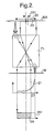
- this translational degree of freedom is exploited to establish a decentered imaging of a pattern: see Fig. 2.
- a projection system PL of a scanning lithography apparatus is shown in Fig. 2 and is assumed to exhibit a strong asymmetric distribution 21 of, for instance, Z 7( x,y ) along the x -direction.
- Such an asymmetry may be caused by residual manufacturing errors that occurred during the manufacturing of the projection system, and is known to be an important contributor to the lithographic error Left-Right asymmetry (LR asymmetry).
- the merit function S will comprise a weighted term which accounts for LR asymmetry (with a weight w chosen by the lithographer):
- the compensation 231 affects, in this embodiment, the relative position of the boundary 29 of the grid of x,y field points (that contribute to the merit function) with respect to the boundary 291 of the full field target portion.
- displacement-compensation means are used to minimize the X, Y and Z image displacements resulting from, for instance, aberration in the lens. Effectively the plane of the image and the wafer is shifted to balance aberration effects of the lens. Alternatively, or in addition, the aberration of the lens itself can be adjusted. For example, spherical aberration adjustment and comatic aberration adjustment can be provided (spherical and comatic aberration are the lowest order even and odd aberrations, respectively). In other respects, this embodiment is the same as Embodiment 1.
- Aberration adjustment will influence the distribution of all aberrations (i.e. change the values of the Zernike coefficients), so will need to be taken into account at step 1.
- the means of adjusting the aberration may also influence the sensitivity coefficients Ai, Bi, Ci, Di, so may need to be taken into account in step 2.
- Lens manipulation primarily influences the low order Zernike aberrations (Z2, Z3, Z4, Z5). The impact of these aberrations on the imaging is displacement and defocus (astigmatism), and this impact is independent of the pattern feature structure and the illumination settings.
- the invention is not limited to reducing overlay and focus errors (minimizing the displacements). Compensation can be used to reduce any lithographic effect that is detrimental to image quality. For example left-right asymmetry (LR asymmetry) caused by 3-wave aberration can be reduced by introducing linear comatic aberration within the system. In other words, increasing one aberration can be used to decrease another aberration such that, on balance, the quality as a whole of a printed feature is improved. It is then necessary to include LR asymmetry in the merit function.
- LEj,j 1,2,3,4,...
- LRasymmetry in the merit function with a weight w 5, to be chosen by the lithographer:
- the sensitivity coefficients for the lithographic error LRasymmetry ( x,y ) in analogy to equations (4) - (7), and proceed as in embodiment 1.
- Another example of a lithographic error which can be compensated for is the error known as Bossung tilt (also known as "iso-focal tilt"). It may occur when a phase shift mask (PSM) is used as patterning means. Ideally, the phase shift between the regions of the mask is precisely 180 degrees.
- PSM phase shift mask
- Q is a sensitivity coefficient.
- a compensation means which is known primarily to affect Z 9 can now be used for counteracting the lithographic error Bossung tilt. If an optimal compromise between correcting for Bossung tilt, LR asymmetry, and the image shifts mentioned in embodiment 1 is to be found, the merit function shall be chosen to be
Landscapes
- Physics & Mathematics (AREA)
- General Physics & Mathematics (AREA)
- Exposure And Positioning Against Photoresist Photosensitive Materials (AREA)
- Exposure Of Semiconductors, Excluding Electron Or Ion Beam Exposure (AREA)
Priority Applications (1)
| Application Number | Priority Date | Filing Date | Title |
|---|---|---|---|
| EP20020252340 EP1251402B1 (de) | 2001-03-30 | 2002-03-28 | Lithographischer Apparat und Verfahren zur Herstellung einer Vorrichtung |
Applications Claiming Priority (3)
| Application Number | Priority Date | Filing Date | Title |
|---|---|---|---|
| EP01303036 | 2001-03-30 | ||
| EP01303036A EP1246014A1 (de) | 2001-03-30 | 2001-03-30 | Lithographischer Apparat |
| EP20020252340 EP1251402B1 (de) | 2001-03-30 | 2002-03-28 | Lithographischer Apparat und Verfahren zur Herstellung einer Vorrichtung |
Publications (2)
| Publication Number | Publication Date |
|---|---|
| EP1251402A1 true EP1251402A1 (de) | 2002-10-23 |
| EP1251402B1 EP1251402B1 (de) | 2007-10-24 |
Family
ID=26077112
Family Applications (1)
| Application Number | Title | Priority Date | Filing Date |
|---|---|---|---|
| EP20020252340 Expired - Lifetime EP1251402B1 (de) | 2001-03-30 | 2002-03-28 | Lithographischer Apparat und Verfahren zur Herstellung einer Vorrichtung |
Country Status (1)
| Country | Link |
|---|---|
| EP (1) | EP1251402B1 (de) |
Cited By (13)
| Publication number | Priority date | Publication date | Assignee | Title |
|---|---|---|---|---|
| EP1434099A1 (de) * | 2002-11-28 | 2004-06-30 | ASML Netherlands B.V. | Verfahren zur Herstellung einer Vorrichtung |
| DE102004006262A1 (de) * | 2004-02-09 | 2005-09-01 | Infineon Technologies Ag | Abbildungseinrichtung und Verfahren zum Entwerfen und Beschreiben einer Abbildungseinrichtung |
| US7042550B2 (en) | 2002-11-28 | 2006-05-09 | Asml Netherlands B.V. | Device manufacturing method and computer program |
| US7102728B2 (en) | 2002-02-27 | 2006-09-05 | Nikon Corporation | Imaging optical system evaluation method, imaging optical system adjustment method, exposure apparatus and exposure method |
| US7262831B2 (en) | 2004-12-01 | 2007-08-28 | Asml Netherlands B.V. | Lithographic projection apparatus and device manufacturing method using such lithographic projection apparatus |
| EP1975723A1 (de) | 2004-07-08 | 2008-10-01 | ASML Netherlands B.V. | Lithographische Projektionsvorrichtung und Geräteherstellungsverfahren damit |
| US7474384B2 (en) | 2004-11-22 | 2009-01-06 | Asml Holding N.V. | Lithographic apparatus, device manufacturing method, and a projection element for use in the lithographic apparatus |
| US7609362B2 (en) | 2004-11-08 | 2009-10-27 | Asml Netherlands B.V. | Scanning lithographic apparatus and device manufacturing method |
| WO2010034674A1 (en) * | 2008-09-25 | 2010-04-01 | Carl Zeiss Smt Ag | Projection exposure apparatus with optimized adjustment possibility |
| US8107054B2 (en) | 2007-09-18 | 2012-01-31 | Carl Zeiss Smt Gmbh | Microlithographic projection exposure apparatus |
| CN104913730A (zh) * | 2014-03-12 | 2015-09-16 | 南京理工大学 | 一种球面面形旋转平移绝对检测方法 |
| WO2017211538A1 (en) * | 2016-06-09 | 2017-12-14 | Asml Netherlands B.V. | Projection system modelling method |
| WO2018197146A1 (en) | 2017-04-26 | 2018-11-01 | Asml Netherlands B.V. | Device manufacturing method |
Families Citing this family (2)
| Publication number | Priority date | Publication date | Assignee | Title |
|---|---|---|---|---|
| DE102012202536A1 (de) | 2012-02-20 | 2013-08-22 | Carl Zeiss Smt Gmbh | Projektionsbelichtungsverfahren und Projektionsbelichtungsanlage für die Mikrolithographie |
| DE102017209440A1 (de) | 2017-06-02 | 2018-12-06 | Carl Zeiss Smt Gmbh | Projektionsbelichtungsverfahren und Projektionsbelichtungsanlage für die Mikrolithografie |
Citations (3)
| Publication number | Priority date | Publication date | Assignee | Title |
|---|---|---|---|---|
| US5444538A (en) * | 1994-03-10 | 1995-08-22 | New Vision Systems, Inc. | System and method for optimizing the grid and intrafield registration of wafer patterns |
| WO2000031592A1 (en) * | 1998-11-23 | 2000-06-02 | Koninklijke Philips Electronics N.V. | Method of detecting aberrations of an optical imaging system |
| US6115108A (en) * | 1998-12-04 | 2000-09-05 | Advanced Micro Devices, Inc. | Illumination modification scheme synthesis using lens characterization data |
-
2002
- 2002-03-28 EP EP20020252340 patent/EP1251402B1/de not_active Expired - Lifetime
Patent Citations (3)
| Publication number | Priority date | Publication date | Assignee | Title |
|---|---|---|---|---|
| US5444538A (en) * | 1994-03-10 | 1995-08-22 | New Vision Systems, Inc. | System and method for optimizing the grid and intrafield registration of wafer patterns |
| WO2000031592A1 (en) * | 1998-11-23 | 2000-06-02 | Koninklijke Philips Electronics N.V. | Method of detecting aberrations of an optical imaging system |
| US6115108A (en) * | 1998-12-04 | 2000-09-05 | Advanced Micro Devices, Inc. | Illumination modification scheme synthesis using lens characterization data |
Cited By (24)
| Publication number | Priority date | Publication date | Assignee | Title |
|---|---|---|---|---|
| US7102728B2 (en) | 2002-02-27 | 2006-09-05 | Nikon Corporation | Imaging optical system evaluation method, imaging optical system adjustment method, exposure apparatus and exposure method |
| EP1434099A1 (de) * | 2002-11-28 | 2004-06-30 | ASML Netherlands B.V. | Verfahren zur Herstellung einer Vorrichtung |
| US7042550B2 (en) | 2002-11-28 | 2006-05-09 | Asml Netherlands B.V. | Device manufacturing method and computer program |
| DE102004006262A1 (de) * | 2004-02-09 | 2005-09-01 | Infineon Technologies Ag | Abbildungseinrichtung und Verfahren zum Entwerfen und Beschreiben einer Abbildungseinrichtung |
| DE102004006262B4 (de) * | 2004-02-09 | 2006-09-14 | Infineon Technologies Ag | Abbildungseinrichtung und Verfahren zum Entwerfen einer Abbildungseinrichtung |
| DE102004006262B9 (de) * | 2004-02-09 | 2006-12-21 | Infineon Technologies Ag | Abbildungseinrichtung und Verfahren zum Entwerfen einer Abbildungseinrichtung |
| EP1975723A1 (de) | 2004-07-08 | 2008-10-01 | ASML Netherlands B.V. | Lithographische Projektionsvorrichtung und Geräteherstellungsverfahren damit |
| US7609362B2 (en) | 2004-11-08 | 2009-10-27 | Asml Netherlands B.V. | Scanning lithographic apparatus and device manufacturing method |
| US7474384B2 (en) | 2004-11-22 | 2009-01-06 | Asml Holding N.V. | Lithographic apparatus, device manufacturing method, and a projection element for use in the lithographic apparatus |
| US7262831B2 (en) | 2004-12-01 | 2007-08-28 | Asml Netherlands B.V. | Lithographic projection apparatus and device manufacturing method using such lithographic projection apparatus |
| US8107054B2 (en) | 2007-09-18 | 2012-01-31 | Carl Zeiss Smt Gmbh | Microlithographic projection exposure apparatus |
| US8982325B2 (en) | 2007-09-18 | 2015-03-17 | Carl Zeiss Smt Gmbh | Microlithographic projection exposure apparatus |
| US9354524B2 (en) | 2008-09-25 | 2016-05-31 | Carl Zeiss Smt Gmbh | Projection exposure apparatus with optimized adjustment possibility |
| US8203696B2 (en) | 2008-09-25 | 2012-06-19 | Carl Zeiss Smt Gmbh | Projection exposure apparatus with optimized adjustment possibility |
| WO2010034674A1 (en) * | 2008-09-25 | 2010-04-01 | Carl Zeiss Smt Ag | Projection exposure apparatus with optimized adjustment possibility |
| US9052609B2 (en) | 2008-09-25 | 2015-06-09 | Carl Zeiss Smt Gmbh | Projection exposure apparatus with optimized adjustment possibility |
| CN102165371A (zh) * | 2008-09-25 | 2011-08-24 | 卡尔蔡司Smt有限责任公司 | 具有优化的调节可能性的投射曝光设备 |
| US10054860B2 (en) | 2008-09-25 | 2018-08-21 | Carl Zeiss Smt Gmbh | Projection exposure apparatus with optimized adjustment possibility |
| CN104913730A (zh) * | 2014-03-12 | 2015-09-16 | 南京理工大学 | 一种球面面形旋转平移绝对检测方法 |
| WO2017211538A1 (en) * | 2016-06-09 | 2017-12-14 | Asml Netherlands B.V. | Projection system modelling method |
| JP2019518990A (ja) * | 2016-06-09 | 2019-07-04 | エーエスエムエル ネザーランズ ビー.ブイ. | 投影システムモデリング方法 |
| US10678143B2 (en) | 2016-06-09 | 2020-06-09 | Asml Netherlands B.V. | Projection system modelling method |
| WO2018197146A1 (en) | 2017-04-26 | 2018-11-01 | Asml Netherlands B.V. | Device manufacturing method |
| US11061336B2 (en) | 2017-04-26 | 2021-07-13 | Asml Netherlands B.V. | Device manufacturing method |
Also Published As
| Publication number | Publication date |
|---|---|
| EP1251402B1 (de) | 2007-10-24 |
Similar Documents
| Publication | Publication Date | Title |
|---|---|---|
| US6809797B2 (en) | Lithographic apparatus, device manufacturing method, and device manufactured thereby | |
| EP1626310B1 (de) | Lithographischer Apparat und Methode zur Herstellung einer Vorrichtung | |
| US20050136340A1 (en) | Lithographic apparatus and methods, patterning structure and method for making a patterning structure, device manufacturing method, and device manufactured thereby | |
| US7262831B2 (en) | Lithographic projection apparatus and device manufacturing method using such lithographic projection apparatus | |
| US7580113B2 (en) | Method of reducing a wave front aberration, and computer program product | |
| USRE43643E1 (en) | Lithographic manufacturing process, lithographic projection apparatus, and device manufactured thereby | |
| US6563564B2 (en) | Method of operating an optical imaging system, lithographic projection apparatus, device manufacturing method, and device manufactured thereby | |
| US6787789B2 (en) | Method of measuring aberration of a projection system of a lithographic apparatus, device manufacturing method, and device manufactured thereby | |
| US20020008869A1 (en) | Method of measuring aberration in an optical imaging system | |
| US7655368B2 (en) | Method for exposing a substrate and lithographic projection apparatus | |
| EP1251402B1 (de) | Lithographischer Apparat und Verfahren zur Herstellung einer Vorrichtung | |
| US7889316B2 (en) | Method for patterning a radiation beam, patterning device for patterning a radiation beam | |
| EP1128217B1 (de) | Verfahren zur Aberrationsmessung in einem optischen Abbildungssystem | |
| US6897947B1 (en) | Method of measuring aberration in an optical imaging system | |
| EP1248154A1 (de) | Lithographisches Herstellungsverfahren und lithographischer Projektionsapparat | |
| US7379156B2 (en) | Lithographic apparatus and device manufacturing method | |
| EP1164436A2 (de) | Betriebsweise eines lithographischen Projektionsapparates | |
| US20060139610A1 (en) | Lithographic apparatus and device manufacturing method | |
| EP1286223A1 (de) | Verfahren zur Messung der Aberration eines lithographischen Projektionssystems | |
| US7663741B2 (en) | Lithographic apparatus, device manufacturing method, calibration method and computer program product | |
| Stoeldraijer et al. | A high throughput DUV wafer stepper with flexible illumination source |
Legal Events
| Date | Code | Title | Description |
|---|---|---|---|
| PUAI | Public reference made under article 153(3) epc to a published international application that has entered the european phase |
Free format text: ORIGINAL CODE: 0009012 |
|
| AK | Designated contracting states |
Kind code of ref document: A1 Designated state(s): AT BE CH CY DE DK ES FI FR GB GR IE IT LI LU MC NL PT SE TR |
|
| AX | Request for extension of the european patent |
Free format text: AL;LT;LV;MK;RO;SI |
|
| 17P | Request for examination filed |
Effective date: 20030416 |
|
| AKX | Designation fees paid |
Designated state(s): DE FR GB IT NL |
|
| 17Q | First examination report despatched |
Effective date: 20040301 |
|
| RAP1 | Party data changed (applicant data changed or rights of an application transferred) |
Owner name: ASML NETHERLANDS B.V. |
|
| RTI1 | Title (correction) |
Free format text: LITHOGRAPHIC APPARATUS AND DEVICE MANUFACTURING METHOD |
|
| GRAP | Despatch of communication of intention to grant a patent |
Free format text: ORIGINAL CODE: EPIDOSNIGR1 |
|
| GRAS | Grant fee paid |
Free format text: ORIGINAL CODE: EPIDOSNIGR3 |
|
| GRAA | (expected) grant |
Free format text: ORIGINAL CODE: 0009210 |
|
| AK | Designated contracting states |
Kind code of ref document: B1 Designated state(s): DE FR GB IT NL |
|
| REG | Reference to a national code |
Ref country code: GB Ref legal event code: FG4D |
|
| REF | Corresponds to: |
Ref document number: 60223102 Country of ref document: DE Date of ref document: 20071206 Kind code of ref document: P |
|
| PGFP | Annual fee paid to national office [announced via postgrant information from national office to epo] |
Ref country code: GB Payment date: 20080320 Year of fee payment: 7 Ref country code: IT Payment date: 20080322 Year of fee payment: 7 Ref country code: NL Payment date: 20080318 Year of fee payment: 7 |
|
| ET | Fr: translation filed | ||
| PLBE | No opposition filed within time limit |
Free format text: ORIGINAL CODE: 0009261 |
|
| STAA | Information on the status of an ep patent application or granted ep patent |
Free format text: STATUS: NO OPPOSITION FILED WITHIN TIME LIMIT |
|
| 26N | No opposition filed |
Effective date: 20080725 |
|
| GBPC | Gb: european patent ceased through non-payment of renewal fee |
Effective date: 20090328 |
|
| NLV4 | Nl: lapsed or anulled due to non-payment of the annual fee |
Effective date: 20091001 |
|
| PG25 | Lapsed in a contracting state [announced via postgrant information from national office to epo] |
Ref country code: NL Free format text: LAPSE BECAUSE OF NON-PAYMENT OF DUE FEES Effective date: 20091001 |
|
| PG25 | Lapsed in a contracting state [announced via postgrant information from national office to epo] |
Ref country code: GB Free format text: LAPSE BECAUSE OF NON-PAYMENT OF DUE FEES Effective date: 20090328 |
|
| PG25 | Lapsed in a contracting state [announced via postgrant information from national office to epo] |
Ref country code: IT Free format text: LAPSE BECAUSE OF NON-PAYMENT OF DUE FEES Effective date: 20090328 |
|
| REG | Reference to a national code |
Ref country code: FR Ref legal event code: PLFP Year of fee payment: 15 |
|
| REG | Reference to a national code |
Ref country code: FR Ref legal event code: PLFP Year of fee payment: 16 |
|
| REG | Reference to a national code |
Ref country code: FR Ref legal event code: PLFP Year of fee payment: 17 |
|
| PGFP | Annual fee paid to national office [announced via postgrant information from national office to epo] |
Ref country code: FR Payment date: 20190322 Year of fee payment: 18 Ref country code: DE Payment date: 20190321 Year of fee payment: 18 |
|
| REG | Reference to a national code |
Ref country code: DE Ref legal event code: R119 Ref document number: 60223102 Country of ref document: DE |
|
| PG25 | Lapsed in a contracting state [announced via postgrant information from national office to epo] |
Ref country code: DE Free format text: LAPSE BECAUSE OF NON-PAYMENT OF DUE FEES Effective date: 20201001 Ref country code: FR Free format text: LAPSE BECAUSE OF NON-PAYMENT OF DUE FEES Effective date: 20200331 |