EP1252784B1 - Interface entre modem et module d'interface d'abonne - Google Patents
Interface entre modem et module d'interface d'abonne Download PDFInfo
- Publication number
- EP1252784B1 EP1252784B1 EP01910408A EP01910408A EP1252784B1 EP 1252784 B1 EP1252784 B1 EP 1252784B1 EP 01910408 A EP01910408 A EP 01910408A EP 01910408 A EP01910408 A EP 01910408A EP 1252784 B1 EP1252784 B1 EP 1252784B1
- Authority
- EP
- European Patent Office
- Prior art keywords
- sim
- circuit
- uart
- clock
- modem
- Prior art date
- Legal status (The legal status is an assumption and is not a legal conclusion. Google has not performed a legal analysis and makes no representation as to the accuracy of the status listed.)
- Expired - Lifetime
Links
- 238000000034 method Methods 0.000 claims description 38
- 230000004044 response Effects 0.000 claims description 28
- 238000004891 communication Methods 0.000 claims description 25
- 238000005070 sampling Methods 0.000 claims description 3
- 238000010586 diagram Methods 0.000 description 21
- 238000004590 computer program Methods 0.000 description 9
- 230000008569 process Effects 0.000 description 8
- 230000006870 function Effects 0.000 description 4
- 230000001413 cellular effect Effects 0.000 description 3
- 230000003287 optical effect Effects 0.000 description 3
- 240000007320 Pinus strobus Species 0.000 description 2
- 230000007246 mechanism Effects 0.000 description 2
- 208000007944 Nodular Nonsuppurative Panniculitis Diseases 0.000 description 1
- 239000013078 crystal Substances 0.000 description 1
- 239000000835 fiber Substances 0.000 description 1
- 238000010295 mobile communication Methods 0.000 description 1
- 238000012163 sequencing technique Methods 0.000 description 1
- 230000003068 static effect Effects 0.000 description 1
- 230000001360 synchronised effect Effects 0.000 description 1
- 230000007704 transition Effects 0.000 description 1
Images


Classifications
-
- H—ELECTRICITY
- H04—ELECTRIC COMMUNICATION TECHNIQUE
- H04M—TELEPHONIC COMMUNICATION
- H04M1/00—Substation equipment, e.g. for use by subscribers
- H04M1/72—Mobile telephones; Cordless telephones, i.e. devices for establishing wireless links to base stations without route selection
- H04M1/725—Cordless telephones
-
- H—ELECTRICITY
- H04—ELECTRIC COMMUNICATION TECHNIQUE
- H04M—TELEPHONIC COMMUNICATION
- H04M11/00—Telephonic communication systems specially adapted for combination with other electrical systems
- H04M11/06—Simultaneous speech and data transmission, e.g. telegraphic transmission over the same conductors
Definitions
- the present invention relates generally to wireless communication devices, and more particularly, to such a wireless communication device including a Subscriber Identity Module.
- SIM Subscriber Identity Module
- WCD Wireless Communication Device
- a conventional SIM includes a small computer system having a controller and a memory.
- the SIM memory contains information related to a subscriber/user of the WCD, including, for example, a subscriber/user identifier, a phonebook identifying a stored bank of telephone numbers, messages, encryption sequences for secured data communications over the air, and so on.
- a subscriber can install the SIM in or remove the SIM from the WCD.
- the SIM can be removed from a first WCD and installed in a second WCD, thereby allowing the user the flexibility of being able to essentially transport his or her "identity" between WCDs.
- a conventional SIM includes a relatively simple electrical interface, including a SIM I/O port for transmitting serialized data to and receiving serialized data from another device (such as a WCD), a SIM clock input for receiving a clock, and reset input for receiving a reset signal.
- functionally interfacing with the conventional SIM can be complicated because the SIM has a processor, and because there are various existing standards (such as the Global System for Mobile Communications (GSM) standards) generally requiring a relatively elaborate scheme for communicating with a SIM. Therefore, functionally interfacing with the SIM through a functional SIM interface is more complicated than just reading data from a memory, for example. Instead, the SIM and a requesting device connected thereto (for example, the WCD) actually exchange commands and responses in a back-and-forth fashion. Further complicating matters is the fact that some SIMs do not comply with generally accepted SIM interface standards (such as GSM).
- EP 0 926 619 A1 provides an interface in which a smartcard receives a clock signal with a frequency set according to any of a predetermined range of operating speeds to improve communicating speed.
- the data transfer between the smartcard and the interface is synchronous with the interface clock and the smartcard communication speed, and the processing speed of the interface serialising means are automatically set when adjusting the interface clock speed.
- the present invention provides a method and circuit for interfacing a modem in a WCD to a SIM.
- the SIM includes an Input/Output(I/O) port for transmitting and receiving serial data, a clock input for receiving a SIM clock, and a reset input for receiving a reset signal.
- the present invention comprises a circuit for interfacing the modem to the SIM.
- the circuit comprises a modem controller and a Universal Asynchronous Receiver/Transmitter (UART) connected to the modem controller.
- the UART includes a transmitter and a receiver to respectively transmit data to and receive data from the SIM I/O port over a common data line.
- the circuit also includes a programmable clock circuit adapted to generate the SIM clock and the UART clock based on a common clock provided to the programmable clock circuit.
- the programmable clock circuit is adapted to generate the SIM clock and the UART clock independently of one another in response to a clock control signal from the modem controller and is further adapted to selectively enable and disable the SIM clock independently of the UART clock in response to a SIM clock enable/disable control signal.
- the modem controller, the UART, and the programmable clock circuit are each constructed on the same integrated circuit (IC) chip.
- the modem controller is adapted to configure the UART to operate in a byte mode wherein the UART receiver collects serialized data bytes from the UART transmitter or the SIM I/O port when transmitted at a programmable baud rate.
- the modem controller is adapted to configure the UART to operate in a sample mode wherein the UART receiver repetitively samples a signal state of the common data line at a sample rate that is a multiple of the programmable baud rate so as to collect sample data bytes.
- the modem controller is further adapted to read the sample data bytes and to detect error conditions related to the SIM based on the sample data bytes collected by the UART receiver.
- the circuit includes a reset circuit adapted to derive and selectively assert and de-assert the SIM reset signal in response to a SIM reset control signal from the modem controller.
- the SIM I/O port is configured as an open-drain I/O port and the common data line is connected between the SIM I/O port and the UART receiver.
- the circuit further comprises a Bus I/F circuit having an input coupled to the UART transmitter and an output coupled to the common data line.
- the Bus I/F circuit is adapted to present a high-impedance to the common data line when the transmitter applies a first logic level to the input of the open drain interface circuit, and a low impedance to signals on the common data line when the transmitter applies a second logic level to the input of the open drain interface circuit.
- the circuit comprises a first power switch connected between a power supply rail of the WCD used to supply power to the Bus I/F circuit and a power input of the Bus I/F circuit.
- the first power switch is adapted to selectively connect and disconnect the WCD power supply rail to the power input of the Bus I/F circuit in response to a first switch control signal.
- the circuit also comprises a first switch control circuit adapted to derive the first switch control signal in response to a first control signal from the modem controller, whereby the modem controller can selectively apply power to and remove power from the SIM.
- the circuit comprises a second power switch connected between a power supply rail of the WCD used to supply power to the SIM and a power input of the SIM.
- the second power switch is adapted to selectively connect and disconnect the WCD power supply rail to the SIM power input in response to a second switch control signal.
- the circuit further comprises a second switch control circuit adapted to derive the second switch control signal in response to a second control signal from the modem controller, whereby the modem controller can selectively apply power to and remove power from the SIM.
- the circuit comprises an interval timer adapted to generate an interrupt to the modem controller after a programmable delay time based on a clock received by the interval timer and in accordance with a delay control signal from the modem controller.
- the present invention comprises a method of interfacing the modem to the SIM.
- the method comprises configuring the UART to operate in the sample mode and transmitting a byte to the SIM over the common line using the UART transmitter.
- the method further comprises repetitively sampling a state of the common line during an error signal window occurring after the byte has been transmitted, thereby collecting sample bytes indicative of whether an error related to the SIM has occurred.
- the method further comprises determining whether the error related to the SIM has occurred based on the sample bytes, and re-transmitting the byte to the SIM when it is determined that the error related to the SIM has occurred.
- the present invention provides an interface, including a method and circuit, for interfacing a WCD to a SIM both electrically and functionally, whereby the WCD can control and access information contained in the SIM.
- the interface is sufficiently flexible as to enable the WCD to interface with a SIM that complies with generally accepted SIM interface standards, and a SIM that does not comply with such standards.
- the interface includes a plurality of interface circuits constructed on a single integrated circuit chip, thereby reducing part count, size, and power requirements in the WCD.
- the interface re-uses circuits and capabilities of a modem of the WCD, including a modem controller, instead of adding a dedicated controller to implement and control the interface, thereby further reducing the part count of and conserving power in the WCD.
- the interface provides data connectivity between the modem and the SIM through a modem UART.
- the interface derives and controls a UART clock and a SIM clock independently of one another.
- the interface derives and controls a SIM reset signal independently of the SIM and UART clocks.
- the interface has the flexibility to initialize and/or reset the logic in the SIM, detect error conditions transmitted by the SIM, detect when the SIM has been installed in and removed from the WCD, and so on.
- the interface includes a Bus interface circuit connected between the modem and the SIM, thereby enabling the modem and the SIM to share a common data line used for communicating data between the two devices.
- the interface can repetitively sample the common data line in a sample mode to detect error conditions associated with the SIM.
- the interface can sample the common data line in a byte mode, thereby collecting data bytes or characters communicated on the common data line.
- the interface can selectively apply power to and remove power from the Bus interface circuit, thereby conserving power in the WCD and protecting the SIM and modem when the SIM is not in use.
- the interface can selectively apply power to and remove power from the SIM, thereby further conserving power in the WCD.
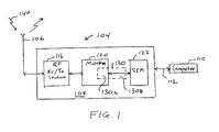
- FIG. 1 is a block diagram of an example WCD 104 in which the present invention can be implemented.
- WCD 104 include a cellular radiotelephone, a satellite radiotelephone, a PCMCIA card incorporated within a computer, and so on.
- WCD 104 includes a transmit/receive antenna 106 and a signal processing module 108 coupled to antenna 106.
- WCD 104 can be coupled to a computer 110 by a datalink 112.
- Signal processing module 108 includes a Radio Frequency (RF) receive (Rx) and transmit (Tx) section 116, a modem 120, and a conventional SIM 122 adapted to be installed in (for example, plugged into) and removed (for example, un-plugged) from signal processing module 108.
- Modem 120 includes a demodulator/decoder section and an encoder/modulator section, both coupled to RF Rx/Tx section 116.
- Modem 120 also includes a modem controller for controlling the modem and SIM 122, as will be described in detail below.
- Conventional SIM 122 includes a small computer system having a controller and a memory.
- the SIM memory contains information related to a subscriber/user of WCD 104, including, for example, a subscriber/user identifier, a phonebook identifying a stored bank of telephone numbers, messages, encryption sequences for secured data communications over the air, and so on.
- the present invention can be used with a SIM compliant with the following standards: ISO/IEC 7816, TIA/EIA IS-820, GSM 11.11, and GSM 11.12.
- the present invention is not limited to use with such a SIM, and can thus be used with a SIM that does not strictly comply with such standards.
- Signal processing module 108 also includes a SIM Interface (I/F) 130 (depicted in dotted line in FIG. 1 ), constructed and operated in accordance with the principles of the present invention, for interfacing modem 120 to SIM 122.
- SIM I/F 130 includes an internal SIM I/F 130a within or internal to modem 120.
- SIM I/F 130 also includes an external SIM I/F 130b external to modem 120.
- Modem 120 can control and access the information contained in SIM 122 through SIM I/F 130, in a manner to be described in detail below.
- antenna 106 of WCD 104 receives an RF signal 140 transmitted from another wireless communication device (not shown), such as a base station, mobile device, and so on.
- RF signal 140 can comply with any number of communication protocols including, for example, a Code Division Multiple Access (CDMA) communication protocol.
- CDMA Code Division Multiple Access
- RF signal 140 can carry information formatted in accordance with a data protocol, such as TCP/IP (Transaction Control Protocol/Internet Protocol).
- Antenna 106 provides RF signal 140 to RF Rx/Tx section 116.
- RF section 116 frequency down-converts the received RF signal, and provides a frequency down-converted signal, such as an Intermediate Frequency (IF) or a baseband signal, to the demodulator/decoder section of modem 120.
- the demodulator/decoder section demodulates and then decodes the down-converted signal to produce a demodulated and decoded signal, available for use in WCD 104 or computer 110, for example.
- the modulator/encoder section of modem 120 encodes and modulates data to be wirelessly transmitted to a remote device, and provides an encoded and modulated baseband or IF signal to RF Rx/Tx section 116.
- RF Rx/Tx section 116 frequency up-converts the baseband or IF signal to produce an RF transmit signal.
- RF Rx/Tx section 116 provides the RF transmit signal to antenna 106, to be wirelessly transmitted by the antenna.
- FIG. 2A is a block diagram of external SIM I/F 130b, according to an embodiment of the present invention.
- external SIM I/F 130b is depicted in relation to both modem 120 and conventional SIM 122.
- Conventional SIM 122 includes a SIM Input/Output (I/O) port 206 to transmit serial data bits to and receive serial data bits from modem 120, a SIM clock input 208, and a SIM reset input 210.
- I/O SIM Input/Output
- SIM I/O port 206 can transmit a data signal, including serial data bits, to a receive port (labeled "RX") of modem 120 over a common data line 212 connected between the SIM I/O port and the modem RX port.
- Modem 120 includes a transmit port (labeled "TX") to transmit a data signal, including serial data bits, to SIM I/O port 206.
- the modem TX port transmits the data signal to I/O port 206 through a Bus I/F circuit 214 having an input connected to the modem TX port and an output connected to common data line 212.
- the modem TX port first transmits the data signal to the Bus I/F circuit input, and in response, the Bus I/F circuit output transmits the data signal to SIM I/O 206 over common data line 212. Therefore, modem 120 transmits serial data to and receives serial data from SIM I/O port 206 over common data line 212. In the present invention, modem 120 and SIM I/O port 206 can safely share common data line 212 because of Bus I/F circuit 214, as will be described in further detail below.
- Modem 120 derives a SIM clock ("SIM_CLK”) at a modem output labeled "CLK” in FIG. 2A , and transmits the SIM clock to SIM input 208 over a clock line 220.
- SIM_CLK SIM clock
- the SIM clock drives logic within SIM 122.
- Modem 120 can selectively enable and disable the SIM clock to control SIM 122.
- Modem 120 derives a SIM reset signal ("SIM RST") at a modem output labeled "RST” in FIG. 2A , and transmits the SIM reset signal to SIM reset input 210 over a reset line 222.
- the SIM reset signal can be used to reset SIM 122.
- Modem 120 can selectively assert and de-assert the SIM reset signal to control SIM 122.
- a first power supply rail 230 external to modem 120 supplies power to a power supply input of SIM 122 through a SIM power switch 232.
- Power switch 232 can selectively apply power to and remove the power from SIM 122 in response to a SIM power control signal provided to switch 232 over a line 234.
- Modem 120 derives the SIM power control signal at a first power enable output of modem 120 (labeled "PWR EN1"), whereby the modem can selectively power-on and power-off SIM 122 to conserve power when SIM 122 is not in use.
- An exemplary switching circuit for power switch 232 includes a FET transistor having a source-drain current path connected between power supply rail 230 and the power supply input of SIM 122, and a gate electrode connected to line 234.
- a second external power supply rail 240 (labeled “Bus V DD ”) supplies power to a power supply input of Bus I/F circuit 214 through a Bus power switch 244.
- Power supply rails 230 and 240 can be the same or different power supply rails.
- Power switch 244 can apply power to and remove the power from Bus I/F circuit 214 in response to a Bus power control signal provided to switch 244 over a line 248.
- Modem 120 derives the Bus power control signal at a second power enable output of modem 120 (labeled "PWR EN2"), whereby the modem can selectively power-on and power-off Bus I/F circuit 214 to further conserve power and protect SIM and modem circuits in the present invention.
- Power switch 244 can include a switching circuit similar to that of switch 234, described above.
- external SIM I/F 130b includes power switches 232 and 244, Bus I/F circuit 214, and the various signal lines 234, 248, 212, 220, and 222, and so on, necessary for conveying the above mentioned interface signals (for example, SIM_CLK, SIM_RST, data signals, and power control signals) between modem 120 and SIM 122.
- interface signals for example, SIM_CLK, SIM_RST, data signals, and power control signals
- SIM I/O port 206 is configured as an open-drain output. Such open-drain outputs are known in the art. Therefore, common line 212, attached to SIM I/O port 206, is referred to herein as an open-drain bus.
- Bus I/F circuit 214 provides a mechanism by which either modem 120 or SIM 122 can drive common line 212 (the open-drain bus) to a desired voltage level without damaging the other device sharing the common line, as is now described.
- the modem transmit and receive ports TX and RX each have a dedicated function.
- the modem transmit port TX includes a drive circuit to actively drive a line attached thereto to either a high or low voltage level (corresponding to a logic high "1” or a logic low "0" binary value, for example).
- the modem receive port RX can sense (that is, sample) a voltage level on common line 212 and translate the level to either a logic high "1" or a logic low "0" binary value.
- the RX port cannot sense the level (that is, state) of the TX port unless a physical connection exists between the RX and TX ports.
- TX port drive circuit actively drives the line attached thereto
- another device attached to and driving the same line in a manner conflicting with the TX port may cause damage to the TX port drive circuit and/or result in unnecessary current draw.
- connecting SIM I/O port 206 directly to the modem TX port could result in a condition where the modem TX port is driving a high logic level while SIM I/O port 206 is driving a low logic level by, for example, providing a low resistance path to ground. Since a potential difference exists across such a low resistance path to ground, SIM I/O port 206 may sink a high current from the modem TX port under the aforementioned condition. As a result, damage to either modem 106 or SIM 122 may occur.
- Bus I/F 214 adapts the modem TX port to an open-drain bus configuration compatible with SIM I/O port 206.
- Bus I/F 214 operates as follows:
- FIG. 2B is a circuit diagram of an example Bus I/F circuit 260 corresponding to Bus I/F circuit 214.
- a reference label “Rx” (such as “R4") denotes a resistor and a reference label “Qx” (such as "Q1") denotes a transistor.
- Bus I/F circuit 260 includes a first NPN transistor 262 (Q2) and a second NPN transistor 264 (Q4) connected in series with the first NPN transistor. Each of the transistors 262 and 264 is configured as an open-collector inverter.
- an output terminal 266 of Bus I/F circuit 260 (connected to common line 212) presents either a high-impedance or a low-impedance path to ground to signals on the common line, in response to a high or low voltage level, respectively, at an input terminal 270 of the Bus I/F circuit (connected to the modem TX port).
- the two inverter stages corresponding to transistors 262 and 264 are depicted as being identical in FIG. 2A .
- the inverter stages need not be identical.
- the first inverter stage can be a logic inverter implemented in any type of logic, such as TTL or CMOS, for example.
- the second inverter stage can be an N-channel enhancement MOS-FET.
- the use of two inverter stages is not necessary. Any circuit meeting the input/output requirements described above can be used.
- FIG. 3 is a block diagram of internal SIM I/F 130a (depicted in conjunction with external SIM I/F 130b, described above) according to an embodiment of the present invention.
- a plurality of circuits associated with internal SIM I/F 130a are constructed on a single integrated circuit chip 301 within modem 120 (as will be described below), thereby advantageously reducing the size of and part count in WCD 104.
- Internal SIM I/F 130a includes a modem controller 302 (also referred to as a Central Processing Unit (CPU)) coupled to a data bus 304.
- modem controller 302 also referred to as a Central Processing Unit (CPU)
- data bus 304 Associated with data bus 304 are an address bus and data read and write signals (not shown), as would be apparent to one of ordinary skill in the art.
- Modem controller 302 is preferably a 32-bit controller (such as a 32-bit Reduced Instruction Set Controller), and correspondingly, data bus 304 is preferably a 32-bit bus.
- Modem controller 302 can write data and/or commands (also referred to as control signals) to other circuit components (described below) coupled to data bus 304. Modem controller 302 can also read data from the other circuit components, as and when appropriate. Modem controller 302 can access (for example, write to and/or read from) the various other components coupled to data bus 304 using a memory mapped access technique, an I/O port access technique, or any other access techniques, as would be apparent to one of ordinary skill in the art.
- Modem controller 302 can receive one or more interrupt signals 306 each associated with a different interrupt condition from the various circuit components coupled to data bus 304, as will be further described below.
- the particular mechanisms associated with receiving an interrupt are well known in the art, and thus will not be described further.
- Modem controller 302 controls circuits and functions in modem 104 not directly associated with interfacing modem 104 to SIM 122, such as demodulating/decoding, encoding/modulating, and transferring data within modem 104 and between the modem and external devices, such as computer 110.
- the present invention reuses modem controller 302 as a SIM interface controller. This beneficially avoids adding a separate controller dedicated to controlling the SIM interface, thereby reducing power consumption, cost and part count in WCD 104, while advantageously maintaining a flexible and powerful SIM interface.
- Internal SIM I/F 130a further includes a SIM power control circuit 308, a Bus power control circuit 310, a UART 312, a UART clock circuit 314, a SIM clock circuit 316, an interval timer 318, and a SIM reset circuit 320, each coupled to data bus 304.
- SIM power control circuit 308 derives the SIM power control signal (mentioned above in connection with FIG. 2A ) in response to a SIM power control signal 330 (also referred to as a command 330) received from modem controller 302, whereby modem controller 302 can power-on and power-off SIM 122.
- SIM power control signal 330 also referred to as a command 330
- Bus power control circuit 310 derives the Bus power control signal (also mentioned above in connection with FIG. 2A ) in response to a Bus power control signal 332 received from modem controller 302, whereby modem controller 302 can power-on and power-off Bus I/F circuit 214.
- Control circuits 308 and 310 can be latched to latch data values ("0" or "1") provided thereto over data bus 304.
- one or both of power switches 232 and 244, and their associated control circuits 308 and 310 are eliminated.
- switch 232 and power rail 230 depicted in FIG. 2A can be omitted.
- switch 244 selectively applies power to both Bus I/F circuit 214 and SIM 122.
- Bus I/F circuit 214 can be constructed on integrated circuit 301, to thus form part of internal I/F 130a instead of external circuit 130b.
- UART 312 includes a UART transmitter 334 (corresponding to the TX port of modem 120) and a UART receiver 336 (corresponding to the RX port of modem 120).
- Modem controller 302 sends UART control signals 338 to UART 312 to configure and control the UART receiver and transmitter 334 and 336.
- modem controller 302 configures a baud rate, number of bits in a character frame (or byte), number of stop bits, and parity (even or odd) used by UART 312.
- UART 312 provides one or more of the interrupt signals 306 to modem controller 302 depending on a state of the UART transmitter 334 and/or receiver 336.
- modem controller 302 can write one or more data bytes 340 to be transmitted to SIM I/O 206, to UART transmitter 334.
- UART transmitter 334 transmits the data bytes in the form of serial data bits to SIM I/O 206 through Bus I/F circuit 214, as mentioned above.
- UART receiver336 can repetitively sample a signal state (that is, a logic level) of common line 212 to collect sample bytes corresponding to the signal state of the common line. Then, modem controller 302 can read the sample bytes (labeled as sample bytes 342 in FIG. 3 ) collected by UART receiver 336, from the UART receiver.
- UART 312 provides an interrupt signal (306) to modem controller 302 indicating the UART has received (and collected sample bytes corresponding to) a data byte transmitted by SIM I/O port 206 or UART transmitter 334, in a manner to be further described below.
- UART 312 receives a UART clock 344 derived or generated by UART clock circuit 314 (described below). UART 312 can transmit and receive serial data at different baud rates determined by UART clock 344 and in accordance with a baud rate control signal (338) received from modem controller 302.
- UART receiver 336 can operate in either of two modes, including a byte mode and a sample mode, according to a mode control command (338) received from modem controller 302.
- UART receiver 336 When commanded to the byte mode, UART receiver 336 receives and collects serialized data bytes transmitted by SIM I/O port 206. To do this, UART receiver 336 samples received serial data bits at a sample rate commensurate with a baud rate at which SIM I/O port 206 (or UART transmitter 334) transmits the serial data bits over common data line 212. Typically, the UART samples each received serial data bit only once or twice in the byte mode. Such operation is conventional.
- UART receiver 336 when commanded to the sample mode, UART receiver 336 repetitively samples common data line 212 at a sample rate many times greater than the baud rate at which SIM I/O port 206 transmits the serial data bits. For example, UART receiver 336 may sample common line 212 at a rate 16X a current baud rate, whereby the UART receiver samples the common line sixteen times during a single serial bit time (of a serial bit transmitted by SIM I/O port 206 or UART transmitter 334). In this example, UART receiver 336 collects sixteen sample bytes per each serial bit transmitted by SIM I/O port 206.
- UART receiver 336 can sample common line 212 in either the sample or byte mode while SIM I/O port 206 or UART transmitter 334 transmits data to common line 212. Therefore, UART receiver 336 can operate in a wrap-around fashion, whereby the receiver samples and collects data transmitted by UART transmitter 334. Also, UART receiver 336 can sample common line 212 when neither SIM I/O port 206 nor UART transmitter 334 transmits data on common line 212.
- Internal SIM I/F 130a receives a common clock 350 from an external clock source 352, such as a crystal oscillator. Exemplary frequencies of common clock 350 include 19.2, 19.68, and 19.8 MHz.
- Programmable UART clock circuit 314, programmable SIM clock circuit 316, and programmable interval timer 318 each receive common clock 350 at respective inputs thereof.
- UART clock circuit 314 derives UART clock 344 based on common clock 350 and in accordance with a UART clock control signal 352 received from modem controller 302.
- UART clock circuit 314 can be a programmable divider to divide the frequency of common clock 350 by a value N according to the UART clock control signal 352, thereby producing UART clock 344 at a controlled frequency.
- SIM clock circuit 316 derives the SIM clock signal based on common clock 350 and in accordance with a first SIM clock (frequency) control signal 354 received from modem controller 302.
- SIM clock circuit 316 can be a programmable divider to divide the frequency of common clock 350 by a value M according to the SIM clock control signal 354, thereby producing the SIM clock at a controlled frequency.
- SIM clock circuit 314 can selectively enable and disable the SIM clock in response to a second SIM clock control (enable/disable) signal 356 received from modem controller 302.
- SIM clock circuit 316 applies a static logic low ("0") or logic high (“1") to reset line 220 in response to receiving a SIM clock disable signal from modem controller 302.
- Interval timer 318 derives a programmable delay time based on common clock 350 and in accordance with a timer control signal 358 received from modem controller 302.
- Interval timer 318 can include a programmable divider and/or counter to count clock cycles of common clock 350.
- modem controller 302 programs interval timer 318 with a delay time. After the delay time has elapsed, interval timer 318 provides a timeout interrupt (306) to modem controller 302, whereby modem controller 302 can keep track of timing associated with controlling SIM 122.
- SIM reset control circuit 320 derives the SIM reset signal in response to a SIM reset control signal 360 received from modem controller 302, whereby modem controller 302 can reset SIM 122.
- SIM reset control circuit 320 can be a latch to latch a data value ("0" or "1") provided thereto.
- FIG. 4 is a series of example timing diagrams (a) through (g) of signals associated with the interface circuit of the present invention.
- Timing diagram (a) represents an example serialized data byte 402 applied to common data line 212 by either SIM I/O port 206 or modem transmitter 334.
- Serialized data byte 402 includes a time-ordered sequence of serial logic bits (each associated with a logic "1” or a logic "0" value or state).
- Serialized data byte 402 includes a start bit "ST"(logic "0"), eight data bits D0 through D7, a parity bit "P,” and one or more stop bits "SP” (logic “1").
- the format of serialized data byte 402 depicted in timing diagram (a) is exemplary only. Other formats, including different numbers of stop bits, for example, are possible.
- SIM 122 When SIM 122 has transmitted a serialized data byte (for example, data byte 402) to or received the same from modem 120, the SIM can indicate an error condition during a period of time 404 referred to as a SIM error window 404, following the stop bit(s) of the serialized data byte. SIM 122 indicates an occurrence of such an error condition by pulsing-low the logic state of common line 212 to logic "0" so as to produce narrow SIM error pulses 406. Each of the SIM error pulses 406 associated with error window 404 are substantially shorter in time than each of the data bits D0-D8.
- Timing diagram (b) is an example time-line 408 indicating when UART receiver 336 samples common data line 212 while the UART receiver is in the sample mode.
- Each of sample strobes 410 and 412 indicate a sampling occurance resulting in a sample byte being collected by UART receiver 336.
- UART receiver 334 can detect the occurance of narrow SIM error pulses 406 because of the relatively high sample rate associated with sample strobes 412. In this way, modem controller 302 can detect one or more bit errors, parity errors, and fault conditions from SIM 122.
- Timing diagram (c) is an example UART interrupt time line 416 corresponding to when UART transmitter 334 transmits serialized data byte 402. After transmitting data byte 402, UART transmitter 334 asserts an interrupt 418 (corresponding to interrupt signal 306) to modem controller 302.
- Timing diagram (d) is an example time line representing consecutive serialized data bytes 422a and 422b transmitted by UART transmitter 334 (or SIM I/O port 206).
- Modem controller 302 imposes a predetermined guardtime 424 between the data bytes 422a and 422b.
- guardtime 424 can be greater than a maximum number of predetermined stop bits associated with each of the data bytes 422a and 422b. Therefore, such guardtimes can be imposed by modem controller 302 using interval timer 318.
- Timing diagram (e) is an example of UART clock 344.
- Timing diagram (f) is an example of the SIM clock (SIM_CLK) depicted in relation to UART clock 344.
- Modem controller 302 can control the SIM clock independently and asynchronously with respect to UART clock 344.
- SIM_CLK includes an initial full clock cycle 430, a beginning portion of a second clock cycle 432, a middle logic low portion 434 corresponding to when SIM_CLK has been disabled by modem controller 302, and a subsequent clock cycle 436 corresponding to when modem controller 302 has re-enabled SIM_CLK.
- modem controller 302 can detect improper bus states of common line 212. Such improper states include common line 212 being "stuck" high or low because SIM 122 is operating improperly, or because the SIM has been removed from, or recently installed in, WCD 104.
- Timing diagram (g) is an example of the SIM reset signal SIM_RST.
- modem controller 302 disables SIM_CLK, transitions SIM_RST from a logic high, to a logic low, and then back to logic high, and then enables SIM_CLK.
- Modem controller 302 uses interval timer 320 to time such asynchronous sequencing of the aforementioned clocks and signals.
- FIG. 5 is a flow chart of an example control method 500 (labeled “Send Byte” in FIG. 5 ) associated with sending (that is, transmitting) a data byte from modem 102 to SIM I/O port 206, according to the present invention.
- modem controller 302 commands UART receiver 336 to the sample mode.
- modem controller 302 transmits a data byte to UART transmitter 334 and commands the UART to transmit the data byte.
- UART transmitter 334 transmits the data byte as serialized data bits to SIM I/O port 206, over common line 212, while UART receiver 336 repetitively samples the common line 212.
- the UART receiver After UART transmitter 334 transmits the data byte, and UART receiver 336 receives the same data byte in the wrap-around fashion described above, the UART receiver provides a receive interrupt (306) to modem controller 302 indicating receipt of the data byte.
- the receive interrupt initiates a next step 506.
- modem controller 302 services the receive interrupt using a receive Interrupt Service Routine (mnemonically referred to as an "Rx ISR").
- modem controller 302 awaits further sample bytes from UART receiver 334.
- FIG. 6 is a flow chart of an example method 600 corresponding to the Rx ISR, mentioned above.
- Method 600 is labeled "Rx ISR" in FIG. 6 , and can be implemented on modem controller 302.
- Method 600 (that is, the Rx ISR) is initiated by a receive interrupt from UART 312.
- a next decision step 606 the sample bytes collected during the error signal window are examined to determine whether an error signal is indicated.
- flow control proceeds to a next step 608.
- a status signal is set to indicate the data byte (mentioned at steps 504 and 604 above) was sent successfully.
- the Rx ISR state is set to "Process guardtime.”
- the process awaits further sample bytes.
- Method steps 604-614 are invoked at step 506 described above in connection with method 500.
- step 606 flow proceeds to a next 614.
- the status signal is set to "re-send,” thereby indicating that the data byte needs to be re-transmitted. Flow then proceeds to step 610.
- next decision step 622 it is determined whether the number of sample bytes received is greater than or equal to the number of sample bytes corresponding to a guardtime. When an insufficient number of sample bytes have been collected, flow proceeds to a next step 624, where more sample bytes are received.
- step 626 UART 312 is reset, and UART receiver 336 is taken out of the sample mode.
- a next data byte can be transmitted using method 500, for example.
- step 632 the last data byte transmitted is re-transmitted using method 500, for example.
- the methods of the present invention are implemented using a controller (for example, modem controller 302) operating in the context of a computer based system.
- a controller for example, modem controller 302
- communication-specific hardware can be used to implement the present invention, the following description of a general purpose computer system is provided for completeness.
- the present invention is preferably implemented in a combination of software executed by modem controller 302, for example, and interface circuitry. Consequently, the invention may be implemented in a computer system or other processing system.
- FIG. 7 An example of such a computer system 700 is shown in FIG. 7 .
- the computer system 700 includes one or more processors, such as processor 704 (corresponding to modem controller 302, for example).
- the processor 704 is connected to a communication infrastructure 706 (for example, a bus or network, which can include data bus 304 discussed in connection with FIG. 3 ).
- a communication infrastructure 706 for example, a bus or network, which can include data bus 304 discussed in connection with FIG. 3 .
- Various software implementations are described in terms of this exemplary computer system. After reading this description, it will become apparent to a person skilled in the relevant art how to implement the invention using other computer systems and/or computer architectures.
- Computer system 700 also includes a main memory 708, preferably random access memory (RAM), and may also include a secondary memory 710.
- the secondary memory 710 may include, for example, a hard disk drive 712 and/or a removable storage drive 714, representing a floppy disk drive, a magnetic tape drive, an optical disk drive, etc.
- the removable storage drive 714 reads from and/or writes to a removable storage unit 718 in a well known manner.
- Removable storage unit 718 represents a floppy disk, magnetic tape, optical disk, etc. which is read by and written to by removable storage drive 714.
- the removable storage unit 718 includes a computer usable storage medium having stored therein computer software and/or data.
- secondary memory 710 may include other similar means for allowing computer programs or other instructions to be loaded into computer system 700.
- Such means may include, for example, a removable storage unit 722 and an interface 720.
- Examples of such means may include a program cartridge and cartridge interface (such as that found in video game devices), a removable memory chip (such as an EPROM, or PROM) and associated socket, and other removable storage units 722 and interfaces 720 which allow software and data to be transferred from the removable storage unit 722 to computer system 700.
- Computer system 700 may also include a communications interface 724.
- Communications interface 724 allows software and data to be transferred between computer system 700 and external devices. Examples of communications interface 724 may include a modem, a network interface (such as an Ethernet card), a communications port, a PCMCIA slot and card, etc.
- Software and data transferred via communications interface 724 are in the form of signals 728 which may be electronic, electromagnetic, optical or other signals capable of being received by communications interface 724. These signals 728 are provided to communications interface 724 via a communications path 726.
- Communications path 726 carries signals 728 and may be implemented using wire or cable, fiber optics, a phone line, a cellular phone link, an RF link and other communications channels.
- computer program medium and “computer usable medium” are used to generally refer to media such as removable storage drive 714, a hard disk installed in hard disk drive 712, and signals 728. These computer program products are means for provi ding software to computer system 700.
- Computer programs are stored in main memory 708 and/or secondary memory 710. Computer programs may also be received via communications interface 724. Such computer programs, when executed, enable the computer system 700 to implement the present invention as discussed herein. In particular, the computer programs, when executed, enable the processor 704 to implement the process of the present invention. Accordingly, such computer programs represent controllers of the computer system 700.
- the processes performed by modem controller 302 can be performed by computer control logic.
- the software may be stored in a computer program product and loaded into computer system 700 using removable storage drive 714, hard drive 712 or communications interface 724.
Landscapes
- Engineering & Computer Science (AREA)
- Computer Networks & Wireless Communication (AREA)
- Signal Processing (AREA)
- Communication Control (AREA)
- Telephonic Communication Services (AREA)
- Mobile Radio Communication Systems (AREA)
- Transceivers (AREA)
Claims (13)
- Circuit (130) pour interfacer un modem (120) dans un dispositif de communication sans fil, WCD, (104) à un module d'interface d'abonné, SIM, (122), le SIM comprenant un port d'entrée/sortie, I/O, (206) pour émettre et recevoir des données en série, et une entrée d'horloge (208) pour recevoir une horloge SIM, comprenant :un contrôleur de modem (302) ;un récepteur/émetteur asynchrone universel, UART, (312) connecté au contrôleur de modem, l'UART comprenant un émetteur (334) et un récepteur (336) pour émettre des données et recevoir des données respectivement vers et en provenance du port I/O du SIM sur une ligne de données commune (212) ; etun circuit d'horloge programmable (316, 314)caractérisé en ce quele circuit d'horloge programmable (316, 314) est adapté à générer l'horloge SIM et l'horloge UART sur la base d'une horloge commune (350) fournie au circuit d'horloge programmable, le circuit d'horloge programmable étant adapté à générer l'horloge SIM et l'horloge UART indépendamment l'une de l'autre en réponse à un signal de commande d'horloge (352, 354, ou 356) provenant du contrôleur de modem ; etle circuit d'horloge programmable (316, 314) est adapté à activer et désactiver sélectivement l'horloge SIM indépendamment de l'horloge UART en réponse à un signal de commande d'activation/désactivation d'horloge SIM (356).
- Circuit selon la revendication 1, dans lequel chacun du contrôleur de modem, de l'UART, et du circuit d'horloge programmable est construit sur la même puce de circuit intégré, IC, (301).
- Circuit selon la revendication 1, dans lequel le circuit d'horloge programmable comprend :un premier diviseur programmable (316) pour générer l'horloge SIM sur la base de l'horloge commune et conformément à un premier signal de commande de fréquence (354) provenant du contrôleur de modem ; etun deuxième diviseur programmable (314) pour générer l'horloge UART sur la base de l'horloge commune et conformément à un deuxième signal de commande de fréquence (352) provenant du contrôleur de modem.
- Circuit selon la revendication 1, dans lequel l'un du port I/O du SIM et de l'émetteur de l'UART est adapté à émettre un multiplet de données sérialisé vers le récepteur de l'UART sur la ligne de données commune, le contrôleur de modem étant adapté à configurer l'UART pour fonctionner dans un mode de multiplets dans lequel le récepteur de l'UART recueille le multiplet de données sérialisé, le contrôleur de modem étant adapté à lire le multiplet de données dans l'UART.
- Circuit selon la revendication 1, dans lequel l'un du port I/O du SIM et de l'émetteur de l'UART est adapté à émettre des bits de données en série vers le récepteur de l'UART sur la ligne de données commune à un débit en bauds prédéterminé, le contrôleur de modem étant adapté à configurer l'UART pour fonctionner dans un mode d'échantillonnage dans lequel le récepteur de l'UART échantillonne de façon répétée l'état du signal de la ligne de données commune à une cadence d'échantillonnage qui est un multiple du débit en bauds prédéterminé de façon à recueillir des multiplets de données échantillonnés, le contrôleur de modem étant adapté à lire les multiplets de données échantillonnés et à détecter des conditions d'erreur associées au SIM sur la base des multiplets de données échantillonnés recueillis par le récepteur de l'UART.
- Circuit selon la revendication 1, dans lequel le SIM comprend une entrée de réinitialisation (210) pour recevoir un signal de réinitialisation SIM, le circuit comprenant en outre un circuit de réinitialisation (320) adapté à déduire et à affirmer et non affirmer sélectivement le signal de réinitialisation SIM en réponse à un signal de commande de réinitialisation SIM (360) provenant du contrôleur de modem.
- Circuit selon la revendication 1, dans lequel le port I/O du SIM est agencé sous la forme d'un port I/O à drain ouvert et la ligne de données commune est connectée entre le port I/O du SIM et le récepteur de l'UART, le circuit comprenant en outre :un circuit d'interface de bus, I/F, (214) ayant une entrée couplée à l'émetteur de l'UART et une sortie couplée à la ligne de données communes, le circuit I/F de bus étant adapté à présenterune haute impédance pour la ligne de données commune lorsque l'émetteur de l'UART applique un premier niveau logique à l'entrée du circuit d'interface I/F de bus, etune basse impédance pour la ligne de données commune lorsque l'émetteur de l'UART applique un deuxième niveau logique à l'entrée du circuit d'interface I/F de bus.
- Circuit selon la revendication 7, comprenant en outre :un commutateur d'alimentation (244) connecté entre un rail d'alimentation du WCD utilisé pour fournir l'alimentation au circuit I/F de bus et une entrée d'alimentation du circuit I/F de bus, le commutateur d'alimentation étant adapté à connecter et déconnecter sélectivement le rail d'alimentation WCD à l'entrée d'alimentation du circuit I/F de bus en réponse à un signal de commande de commutateur ; etun circuit de commande de commutateur (310) adapté à déduire le signal de commande de commutateur en réponse à un signal de commande (332) provenant du contrôleur de modem, d'où il résulte que le contrôleur de modem peut sélectivement appliquer et retirer l'alimentation du circuit I/F de bus.
- Circuit selon la revendication 8, comprenant en outre :un deuxième commutateur d'alimentation (232) connecté entre un rail d'alimentation du WCD utilisé pour fournir l'alimentation au SIM et une entrée d'alimentation du SIM, le deuxième commutateur d'alimentation étant adapté à connecter et déconnecter sélectivement le rail d'alimentation du WCD à l'entrée d'alimentation du SIM en réponse à un deuxième signal de commande de commutateur ; etun deuxième circuit de commande de commutateur (308) adapté à déduire le deuxième signal de commande de commutateur en réponse à un deuxième signal de commande (330) provenant du contrôleur de modem, d'où il résulte que le contrôleur de modem peut sélectivement appliquer et retirer l'alimentation du SIM.
- Circuit selon la revendication 1, comprenant en outre :un commutateur d'alimentation (232) connecté entre un rail d'alimentation du WCD utilisé pour fournir l'alimentation au SIM et une entrée d'alimentation du SIM, le commutateur d'alimentation étant adapté à connecter et déconnecter sélectivement le rail d'alimentation du WCD à l'entrée d'alimentation du SIM en réponse à un signal de commande de commutateur ; etun circuit de commande de commutateur (308) adapté à déduire le signal de commande de commutateur en réponse à un signal de commande (330) provenant du contrôleur de modem, d'où il résulte que le contrôleur de modem peut appliquer et retirer sélectivement l'alimentation du SIM.
- Circuit selon la revendication 1, comprenant en outre un minuteur d'intervalle (318) adapté à générer une interruption (306) vers le contrôleur de modem après un retard programmable sur la base d'une horloge (350) reçue par le minuteur d'intervalle et conformément à un signal de commande de retard (358) provenant du contrôleur de modem.
- Procédé pour interfacer un modem (120) dans un dispositif de communication sans fil, WCD, (104) à un module d'interface d'abonné, SIM, (122), le modem comprenant un contrôleur de modem (302) couplé à un récepteur/émetteur asynchrone universel, UART, (312), l'UART comprenant un émetteur (334) et un récepteur (336) pour émettre des données et recevoir des données respectivement vers et en provenance du SIM sur une ligne de données commune (212) à un ou plusieurs débits en bauds prédéterminés, le récepteur de l'UART étant configurable pour fonctionner soit dans un mode de multiplets dans lequel le récepteur de l'UART recueille des multiplets de données sérialisés qui lui sont transmis à un débit en bauds prédéterminé, soit dans un mode d'échantillonnage dans lequel le récepteur de l'UART échantillonnage l'état de la ligne de données commune à une cadence d'échantillonnage dépassant le débit en bauds prédéterminé,
caractérisé en ce que le procédé comprend les étapes suivantes :(a) configurer l'UART pour fonctionner dans le mode d'échantillonnage (502) ;(b) émettre un multiplet vers le SIM sur la ligne commune en utilisant l'émetteur de l'UART (504) ;(c) échantillonner de façon répétitive l'état de la ligne commune pendant une fenêtre de signal d'erreur survenant après que le multiplet a été transmis dans l'étape (b), recueillant ainsi des multiplets échantillonnés indicatifs du fait qu'une erreur associée au SIM est survenue ou pas ;(d) déterminer si l'erreur associée au SIM est survenue sur la base des multiplets échantillonnés (606) ; et(e) réémettre le multiplet vers le SIM lorsqu'il est déterminé que l'erreur associée au SIM est survenue (614). - Procédé selon la revendication 16, comprenant en outre les étapes suivantes :(f) déterminer le moment où un temps de garde prédéterminé s'est écoulé depuis que le multiplet a été émis à l'étape (b) en comptant d'autres multiplets échantillonnés (620, 622) ; et(g) répéter l'étape (b) lorsque le temps de garde prédéterminé s'est écoulé (630).
Applications Claiming Priority (3)
| Application Number | Priority Date | Filing Date | Title |
|---|---|---|---|
| US18022800P | 2000-02-04 | 2000-02-04 | |
| US180228P | 2000-02-04 | ||
| PCT/US2001/003441 WO2001058191A2 (fr) | 2000-02-04 | 2001-02-02 | Interface entre modem et module d'interface d'abonne |
Publications (2)
| Publication Number | Publication Date |
|---|---|
| EP1252784A2 EP1252784A2 (fr) | 2002-10-30 |
| EP1252784B1 true EP1252784B1 (fr) | 2013-03-20 |
Family
ID=22659695
Family Applications (1)
| Application Number | Title | Priority Date | Filing Date |
|---|---|---|---|
| EP01910408A Expired - Lifetime EP1252784B1 (fr) | 2000-02-04 | 2001-02-02 | Interface entre modem et module d'interface d'abonne |
Country Status (9)
| Country | Link |
|---|---|
| US (1) | US6839570B2 (fr) |
| EP (1) | EP1252784B1 (fr) |
| JP (1) | JP4741149B2 (fr) |
| KR (1) | KR20030072203A (fr) |
| CN (1) | CN1429462A (fr) |
| AU (1) | AU2001238017A1 (fr) |
| CA (1) | CA2409816C (fr) |
| ES (1) | ES2407132T3 (fr) |
| WO (1) | WO2001058191A2 (fr) |
Cited By (1)
| Publication number | Priority date | Publication date | Assignee | Title |
|---|---|---|---|---|
| CN107613098A (zh) * | 2017-08-24 | 2018-01-19 | 广东欧珀移动通信有限公司 | 一种移动终端及其下载模式切换电路、下载模式切换方法 |
Families Citing this family (46)
| Publication number | Priority date | Publication date | Assignee | Title |
|---|---|---|---|---|
| FR2800228B1 (fr) * | 1999-10-26 | 2002-02-08 | Wavecom Sa | Systeme et procede de commande d'un equipement tiers par une carte sim, via un module de radiocommunication, module de radiocommunication et equipement tiers correspondants |
| US7822878B2 (en) * | 2000-02-17 | 2010-10-26 | Siemens Industry, Inc. | Device, system, and method for the automatic configuration of a network communications device |
| EP1304007A1 (fr) * | 2000-05-26 | 2003-04-23 | Cegetel Groupe | Procede de dialogue entre un module d'identification d'abonne, cooperant avec un terminal au sein d'un radiotelephone, et un dispositif local |
| JP2002359660A (ja) * | 2001-03-28 | 2002-12-13 | Sony Computer Entertainment Inc | データ通信装置及び方法、データ通信システム、データ通信プログラムを記録した記録媒体、データ通信プログラム |
| US6895518B2 (en) * | 2001-05-31 | 2005-05-17 | Koninklijke Philips Electronics N.V. | Power and frequency adjustable UART device |
| US20030037191A1 (en) * | 2001-08-13 | 2003-02-20 | Robert Baranowski | Wireless module |
| US6909659B2 (en) * | 2001-08-30 | 2005-06-21 | Micron Technology, Inc. | Zero power chip standby mode |
| US7898994B2 (en) * | 2002-02-25 | 2011-03-01 | Hewlett-Packard Development Company, L.P. | Power saving in multi-processor device |
| US6959349B2 (en) * | 2002-05-17 | 2005-10-25 | Abocom Systems, Inc. | Wireless computer peripheral interface with the capability of identification |
| US7395447B2 (en) * | 2002-09-16 | 2008-07-01 | Silicon Labs Cp, Inc. | Precision oscillator for an asynchronous transmission system |
| US6917658B2 (en) * | 2002-09-16 | 2005-07-12 | Silicon Labs Cp, Inc. | Clock recovery method for bursty communications |
| AU2003272066A1 (en) * | 2002-10-16 | 2004-05-04 | Alon Bear | Smart card network interface device |
| CA2427369A1 (fr) * | 2002-12-24 | 2004-06-24 | Research In Motion Limited | Methodes et appareils permettant de commander l'alimentation des circuits electriques d'un appareil de communications sans fil dote d'une interface de module d'identite d'abonne (sim) |
| US7313177B2 (en) * | 2003-05-10 | 2007-12-25 | Hewlett-Packard Development Company, L.P. | Reset scheme for I/O pads in a source synchronous system |
| EP1665059B1 (fr) * | 2003-09-09 | 2007-01-24 | Siemens Aktiengesellschaft | Circuit servant d'interface entre une carte sim et un modem gsm |
| WO2005027549A1 (fr) * | 2003-09-10 | 2005-03-24 | Siemens Aktiengesellschaft | Prolongement de l'interface a carte sim dans des appareils gsm |
| US7610061B2 (en) * | 2003-09-20 | 2009-10-27 | Samsung Electronics Co., Ltd. | Communication device and method having a common platform |
| DE10357824A1 (de) | 2003-12-09 | 2005-07-14 | Kuka Roboter Gmbh | Verfahren und Vorrichtung zum Betreiben zusammenarbeitender unterschiedlicher Geräte |
| KR20050098142A (ko) * | 2004-04-06 | 2005-10-11 | 삼성전자주식회사 | 직렬 통신 인터페이스를 통해 호스트와 통신하는 전자 장치 |
| TWM266644U (en) * | 2004-10-22 | 2005-06-01 | Uniwill Comp Corp | Wireless conversion device |
| US7707441B2 (en) * | 2004-10-22 | 2010-04-27 | Broadcom Corporation | Method and system for reducing power consumption of handsets through UART auto flow control |
| US20060104227A1 (en) * | 2004-11-15 | 2006-05-18 | Chia-En Chuang | Data communication methods and systems |
| US7581678B2 (en) | 2005-02-22 | 2009-09-01 | Tyfone, Inc. | Electronic transaction card |
| US8913634B2 (en) * | 2005-04-01 | 2014-12-16 | Freescale Semiconductor, Inc. | Method and apparatus facilitating multi mode interfaces |
| CN104486477A (zh) * | 2005-09-08 | 2015-04-01 | 联想创新有限公司(香港) | 移动通信终端和移动通信方法 |
| US7288962B2 (en) * | 2006-02-08 | 2007-10-30 | Kyocera Wireless Corp. | Level shifting multiplexing circuit for connecting a two conductor full duplex bus to a bidirectional single conductor bus |
| TWI324865B (en) * | 2006-03-31 | 2010-05-11 | Hon Hai Prec Ind Co Ltd | Power management system and method for network device |
| US7711373B2 (en) * | 2006-05-11 | 2010-05-04 | Nokia Corporation | Multiradio control interface |
| US20080035729A1 (en) * | 2006-08-09 | 2008-02-14 | Wei-Jung Lin | Multiple Card Reading Modules Apparatus |
| US9741027B2 (en) * | 2007-12-14 | 2017-08-22 | Tyfone, Inc. | Memory card based contactless devices |
| EP2114027A1 (fr) * | 2008-04-30 | 2009-11-04 | Gemplus | Méthode de détection d'un arrêt de l'utilisation de télévision sur un terminal téléphonique |
| US8451122B2 (en) | 2008-08-08 | 2013-05-28 | Tyfone, Inc. | Smartcard performance enhancement circuits and systems |
| US12147863B2 (en) | 2008-08-08 | 2024-11-19 | Icashe, Inc. | Method and apparatus for transmitting data via NFC for mobile applications including mobile payments and ticketing |
| EP2401708A4 (fr) | 2009-02-24 | 2012-08-15 | Tyfone Inc | Dispositif sans contact à antenne miniaturisée |
| US8489837B1 (en) * | 2009-06-12 | 2013-07-16 | Netlist, Inc. | Systems and methods for handshaking with a memory module |
| TWI449356B (zh) * | 2010-02-05 | 2014-08-11 | Htc Corp | 可拆卸的無線通訊模組以及其啟動的方法 |
| CN101859395A (zh) * | 2010-05-14 | 2010-10-13 | 中兴通讯股份有限公司 | 信息传输的实现方法和系统、主控设备、以及智能卡 |
| US8817856B2 (en) * | 2010-05-27 | 2014-08-26 | Lg Electronics Inc. | Method and apparatus for controlling suspend mode in dual modem device |
| KR101679430B1 (ko) * | 2010-09-30 | 2016-11-25 | 삼성전자주식회사 | 휴대단말기에서 심카드의 삽입을 인식하는 방법 및 장치 |
| US8615227B2 (en) * | 2011-12-12 | 2013-12-24 | Broadcom Corporation | Enhanced discontinuous mode operation with shared radio frequency resources |
| CN103581157A (zh) * | 2012-08-10 | 2014-02-12 | 中兴通讯股份有限公司 | 嵌入式设备和基于该设备进行数据通信的控制方法 |
| US8745301B2 (en) * | 2012-10-29 | 2014-06-03 | Qualcomm Incorporated | High voltage dedicated charging port |
| US8760123B2 (en) | 2012-10-29 | 2014-06-24 | Qualcomm Incorporated | High voltage dedicated charging port |
| WO2017049317A1 (fr) * | 2015-09-18 | 2017-03-23 | Able Device, Inc. | Liaison de données sécurisée pour processeur à base de module d'identification d'abonné (sim) |
| WO2019046214A1 (fr) * | 2017-08-28 | 2019-03-07 | Sigma Designs, Inc. | Communications de microcontrôleur externe |
| US12493509B2 (en) * | 2023-11-09 | 2025-12-09 | Nxp Usa, Inc. | Fault interface architecture in safety-relevant systems |
Family Cites Families (10)
| Publication number | Priority date | Publication date | Assignee | Title |
|---|---|---|---|---|
| FI89432C (fi) * | 1991-06-26 | 1993-09-27 | Nokia Mobile Phones Ltd | Genering av en klockfrekvens i ett smart card graenssnitt |
| FR2683342B1 (fr) * | 1991-10-31 | 1994-01-07 | Gemplus Card International | Circuit d'interface pour carte a circuit integre. |
| US5920850A (en) * | 1994-11-04 | 1999-07-06 | Pitney Bowes Inc. | Metering system with automatic resettable time lockout |
| FR2739242B1 (fr) * | 1995-09-25 | 1997-10-24 | Gemplus Card Int | Modem equipe d'un lecteur de carte a puce |
| FR2755566B1 (fr) * | 1996-11-04 | 1998-12-11 | Alsthom Cge Alcatel | Modem radio equipe d'un lecteur de carte a memoire |
| FR2767011B1 (fr) * | 1997-08-04 | 1999-09-24 | Alsthom Cge Alcatel | Procede d'adaptation du fonctionnement d'un module d'identification d'abonne a une ou des interface(s) d'un terminal mobile de radio-communication, module d'identification d'abonne et terminal mobile correspondants |
| FR2772535B1 (fr) * | 1997-12-11 | 2000-12-15 | Micropross | Interface de communication avec une carte a puce synchrone et dispositif equipe d'une telle interface |
| GB2335568B (en) * | 1998-03-18 | 2003-04-09 | Nec Technologies | Network operator controlled locking and unlocking mechanism for mobile phones |
| JPH11340868A (ja) * | 1998-05-29 | 1999-12-10 | Kyocera Corp | 携帯電話機 |
| EP1135732A1 (fr) * | 1998-12-08 | 2001-09-26 | AlliedSignal Inc. | Circuit ameliore universel asynchrone d'emission et de reception dans un systeme de telecommunications par satellite |
-
2001
- 2001-02-02 EP EP01910408A patent/EP1252784B1/fr not_active Expired - Lifetime
- 2001-02-02 ES ES01910408T patent/ES2407132T3/es not_active Expired - Lifetime
- 2001-02-02 KR KR1020027009959A patent/KR20030072203A/ko not_active Withdrawn
- 2001-02-02 AU AU2001238017A patent/AU2001238017A1/en not_active Abandoned
- 2001-02-02 CA CA2409816A patent/CA2409816C/fr not_active Expired - Fee Related
- 2001-02-02 US US09/773,768 patent/US6839570B2/en not_active Expired - Lifetime
- 2001-02-02 WO PCT/US2001/003441 patent/WO2001058191A2/fr not_active Ceased
- 2001-02-02 JP JP2001557315A patent/JP4741149B2/ja not_active Expired - Fee Related
- 2001-02-02 CN CN01807771A patent/CN1429462A/zh not_active Withdrawn
Cited By (2)
| Publication number | Priority date | Publication date | Assignee | Title |
|---|---|---|---|---|
| CN107613098A (zh) * | 2017-08-24 | 2018-01-19 | 广东欧珀移动通信有限公司 | 一种移动终端及其下载模式切换电路、下载模式切换方法 |
| CN107613098B (zh) * | 2017-08-24 | 2020-09-04 | Oppo广东移动通信有限公司 | 一种移动终端及其下载模式切换电路、下载模式切换方法 |
Also Published As
| Publication number | Publication date |
|---|---|
| JP4741149B2 (ja) | 2011-08-03 |
| EP1252784A2 (fr) | 2002-10-30 |
| US20010034246A1 (en) | 2001-10-25 |
| CA2409816C (fr) | 2011-03-15 |
| WO2001058191A3 (fr) | 2002-02-14 |
| WO2001058191A9 (fr) | 2002-10-31 |
| JP2003524331A (ja) | 2003-08-12 |
| WO2001058191A2 (fr) | 2001-08-09 |
| US6839570B2 (en) | 2005-01-04 |
| AU2001238017A1 (en) | 2001-08-14 |
| ES2407132T3 (es) | 2013-06-11 |
| CN1429462A (zh) | 2003-07-09 |
| CA2409816A1 (fr) | 2001-08-09 |
| KR20030072203A (ko) | 2003-09-13 |
Similar Documents
| Publication | Publication Date | Title |
|---|---|---|
| EP1252784B1 (fr) | Interface entre modem et module d'interface d'abonne | |
| US20080245878A1 (en) | Ic card | |
| EP3695320B1 (fr) | Interconnexion de composants périphériques express faible puissance | |
| CN101304356B (zh) | 无线通信终端、半导体器件、数据通信方法和无线通信系统 | |
| TW201702891A (zh) | 具有多重模式調變之增強虛擬gpio | |
| US7337966B2 (en) | Transmission interface | |
| US9880895B2 (en) | Serial interface with bit-level acknowledgement and error correction | |
| US6962293B2 (en) | Circuit for generating clock signal and decoding data signal for use in contactless integrated circuit card | |
| US6412029B1 (en) | Method and apparatus for interfacing between a digital signal processor and a baseband circuit for wireless communication system | |
| US5864300A (en) | Communication system for selecting a communication transmission method | |
| JP5007382B2 (ja) | 無線分離と互換のsimインタフェースを有する通信装置 | |
| US20030037191A1 (en) | Wireless module | |
| US20020013148A1 (en) | Telephone set identifying method, telephone set type identifying apparatus, processing apparatus and storage medium | |
| HK1055054A (en) | Interface between modem and subscriber interface module | |
| CN111624915A (zh) | 一种上位机通过串口唤醒微控制器的方法 | |
| US20030236931A1 (en) | Data transfer control circuitry including fifo buffers | |
| Martín Galicia | Telemetry, Tracking and Command Board Design of a CubeSat | |
| CN119383701A (zh) | 一种低功耗的uart通讯系统及方法 | |
| JP2000227951A (ja) | 電子回路の管理方法 | |
| WO2025141509A1 (fr) | Cœur numérique d'étiquette rfid, interprétateur de démodulation rfid et circuit de préparation et de mise en forme de réponse rfid | |
| TW201702895A (zh) | 具有線活動偵測器之通用非同步接收器/傳輸器 | |
| JPH11275000A (ja) | データ通信カードへの初期登録設定方式 | |
| CN110365687A (zh) | Swp协议处理器 | |
| KR20030020746A (ko) | 무선가입자망 단말기의 모니터링 메시지 전송장치 및 그방법 |
Legal Events
| Date | Code | Title | Description |
|---|---|---|---|
| PUAI | Public reference made under article 153(3) epc to a published international application that has entered the european phase |
Free format text: ORIGINAL CODE: 0009012 |
|
| 17P | Request for examination filed |
Effective date: 20020819 |
|
| AK | Designated contracting states |
Kind code of ref document: A2 Designated state(s): AT BE CH CY DE DK ES FI FR GB GR IE IT LI LU MC NL PT SE TR |
|
| AX | Request for extension of the european patent |
Free format text: AL;LT;LV;MK;RO;SI |
|
| 17Q | First examination report despatched |
Effective date: 20040607 |
|
| REG | Reference to a national code |
Ref country code: DE Ref legal event code: R079 Ref document number: 60147790 Country of ref document: DE Free format text: PREVIOUS MAIN CLASS: H04Q0007320000 Ipc: H04M0001725000 |
|
| RIC1 | Information provided on ipc code assigned before grant |
Ipc: H04M 11/06 20060101ALI20120702BHEP Ipc: H04M 1/725 20060101AFI20120702BHEP |
|
| GRAP | Despatch of communication of intention to grant a patent |
Free format text: ORIGINAL CODE: EPIDOSNIGR1 |
|
| GRAS | Grant fee paid |
Free format text: ORIGINAL CODE: EPIDOSNIGR3 |
|
| GRAA | (expected) grant |
Free format text: ORIGINAL CODE: 0009210 |
|
| AK | Designated contracting states |
Kind code of ref document: B1 Designated state(s): AT BE CH CY DE DK ES FI FR GB GR IE IT LI LU MC NL PT SE TR |
|
| REG | Reference to a national code |
Ref country code: GB Ref legal event code: FG4D |
|
| REG | Reference to a national code |
Ref country code: CH Ref legal event code: EP |
|
| REG | Reference to a national code |
Ref country code: IE Ref legal event code: FG4D |
|
| REG | Reference to a national code |
Ref country code: AT Ref legal event code: REF Ref document number: 602663 Country of ref document: AT Kind code of ref document: T Effective date: 20130415 |
|
| REG | Reference to a national code |
Ref country code: DE Ref legal event code: R096 Ref document number: 60147790 Country of ref document: DE Effective date: 20130516 |
|
| REG | Reference to a national code |
Ref country code: ES Ref legal event code: FG2A Ref document number: 2407132 Country of ref document: ES Kind code of ref document: T3 Effective date: 20130611 |
|
| REG | Reference to a national code |
Ref country code: NL Ref legal event code: T3 |
|
| PG25 | Lapsed in a contracting state [announced via postgrant information from national office to epo] |
Ref country code: SE Free format text: LAPSE BECAUSE OF FAILURE TO SUBMIT A TRANSLATION OF THE DESCRIPTION OR TO PAY THE FEE WITHIN THE PRESCRIBED TIME-LIMIT Effective date: 20130320 |
|
| REG | Reference to a national code |
Ref country code: AT Ref legal event code: MK05 Ref document number: 602663 Country of ref document: AT Kind code of ref document: T Effective date: 20130320 |
|
| PG25 | Lapsed in a contracting state [announced via postgrant information from national office to epo] |
Ref country code: GR Free format text: LAPSE BECAUSE OF FAILURE TO SUBMIT A TRANSLATION OF THE DESCRIPTION OR TO PAY THE FEE WITHIN THE PRESCRIBED TIME-LIMIT Effective date: 20130621 Ref country code: FI Free format text: LAPSE BECAUSE OF FAILURE TO SUBMIT A TRANSLATION OF THE DESCRIPTION OR TO PAY THE FEE WITHIN THE PRESCRIBED TIME-LIMIT Effective date: 20130320 |
|
| PG25 | Lapsed in a contracting state [announced via postgrant information from national office to epo] |
Ref country code: BE Free format text: LAPSE BECAUSE OF FAILURE TO SUBMIT A TRANSLATION OF THE DESCRIPTION OR TO PAY THE FEE WITHIN THE PRESCRIBED TIME-LIMIT Effective date: 20130320 |
|
| PG25 | Lapsed in a contracting state [announced via postgrant information from national office to epo] |
Ref country code: PT Free format text: LAPSE BECAUSE OF FAILURE TO SUBMIT A TRANSLATION OF THE DESCRIPTION OR TO PAY THE FEE WITHIN THE PRESCRIBED TIME-LIMIT Effective date: 20130722 Ref country code: AT Free format text: LAPSE BECAUSE OF FAILURE TO SUBMIT A TRANSLATION OF THE DESCRIPTION OR TO PAY THE FEE WITHIN THE PRESCRIBED TIME-LIMIT Effective date: 20130320 |
|
| PG25 | Lapsed in a contracting state [announced via postgrant information from national office to epo] |
Ref country code: CY Free format text: LAPSE BECAUSE OF FAILURE TO SUBMIT A TRANSLATION OF THE DESCRIPTION OR TO PAY THE FEE WITHIN THE PRESCRIBED TIME-LIMIT Effective date: 20130320 |
|
| PLBE | No opposition filed within time limit |
Free format text: ORIGINAL CODE: 0009261 |
|
| STAA | Information on the status of an ep patent application or granted ep patent |
Free format text: STATUS: NO OPPOSITION FILED WITHIN TIME LIMIT |
|
| PG25 | Lapsed in a contracting state [announced via postgrant information from national office to epo] |
Ref country code: DK Free format text: LAPSE BECAUSE OF FAILURE TO SUBMIT A TRANSLATION OF THE DESCRIPTION OR TO PAY THE FEE WITHIN THE PRESCRIBED TIME-LIMIT Effective date: 20130320 |
|
| 26N | No opposition filed |
Effective date: 20140102 |
|
| REG | Reference to a national code |
Ref country code: DE Ref legal event code: R097 Ref document number: 60147790 Country of ref document: DE Effective date: 20140102 |
|
| PG25 | Lapsed in a contracting state [announced via postgrant information from national office to epo] |
Ref country code: MC Free format text: LAPSE BECAUSE OF FAILURE TO SUBMIT A TRANSLATION OF THE DESCRIPTION OR TO PAY THE FEE WITHIN THE PRESCRIBED TIME-LIMIT Effective date: 20130320 Ref country code: LU Free format text: LAPSE BECAUSE OF FAILURE TO SUBMIT A TRANSLATION OF THE DESCRIPTION OR TO PAY THE FEE WITHIN THE PRESCRIBED TIME-LIMIT Effective date: 20140202 |
|
| REG | Reference to a national code |
Ref country code: CH Ref legal event code: PL |
|
| PG25 | Lapsed in a contracting state [announced via postgrant information from national office to epo] |
Ref country code: LI Free format text: LAPSE BECAUSE OF NON-PAYMENT OF DUE FEES Effective date: 20140228 Ref country code: CH Free format text: LAPSE BECAUSE OF NON-PAYMENT OF DUE FEES Effective date: 20140228 |
|
| REG | Reference to a national code |
Ref country code: IE Ref legal event code: MM4A |
|
| PG25 | Lapsed in a contracting state [announced via postgrant information from national office to epo] |
Ref country code: IE Free format text: LAPSE BECAUSE OF NON-PAYMENT OF DUE FEES Effective date: 20140202 |
|
| REG | Reference to a national code |
Ref country code: FR Ref legal event code: PLFP Year of fee payment: 16 |
|
| PG25 | Lapsed in a contracting state [announced via postgrant information from national office to epo] |
Ref country code: TR Free format text: LAPSE BECAUSE OF FAILURE TO SUBMIT A TRANSLATION OF THE DESCRIPTION OR TO PAY THE FEE WITHIN THE PRESCRIBED TIME-LIMIT Effective date: 20130320 |
|
| REG | Reference to a national code |
Ref country code: FR Ref legal event code: PLFP Year of fee payment: 17 |
|
| REG | Reference to a national code |
Ref country code: FR Ref legal event code: PLFP Year of fee payment: 18 |
|
| PGFP | Annual fee paid to national office [announced via postgrant information from national office to epo] |
Ref country code: NL Payment date: 20180209 Year of fee payment: 18 |
|
| PGFP | Annual fee paid to national office [announced via postgrant information from national office to epo] |
Ref country code: ES Payment date: 20180302 Year of fee payment: 18 |
|
| PGFP | Annual fee paid to national office [announced via postgrant information from national office to epo] |
Ref country code: FR Payment date: 20180118 Year of fee payment: 18 Ref country code: IT Payment date: 20180216 Year of fee payment: 18 |
|
| REG | Reference to a national code |
Ref country code: NL Ref legal event code: MM Effective date: 20190301 |
|
| PG25 | Lapsed in a contracting state [announced via postgrant information from national office to epo] |
Ref country code: NL Free format text: LAPSE BECAUSE OF NON-PAYMENT OF DUE FEES Effective date: 20190301 |
|
| PG25 | Lapsed in a contracting state [announced via postgrant information from national office to epo] |
Ref country code: FR Free format text: LAPSE BECAUSE OF NON-PAYMENT OF DUE FEES Effective date: 20190228 Ref country code: IT Free format text: LAPSE BECAUSE OF NON-PAYMENT OF DUE FEES Effective date: 20190202 |
|
| REG | Reference to a national code |
Ref country code: ES Ref legal event code: FD2A Effective date: 20200327 |
|
| PG25 | Lapsed in a contracting state [announced via postgrant information from national office to epo] |
Ref country code: ES Free format text: LAPSE BECAUSE OF NON-PAYMENT OF DUE FEES Effective date: 20190203 |
|
| PGFP | Annual fee paid to national office [announced via postgrant information from national office to epo] |
Ref country code: DE Payment date: 20200115 Year of fee payment: 20 Ref country code: GB Payment date: 20200130 Year of fee payment: 20 |
|
| REG | Reference to a national code |
Ref country code: DE Ref legal event code: R071 Ref document number: 60147790 Country of ref document: DE |
|
| REG | Reference to a national code |
Ref country code: GB Ref legal event code: PE20 Expiry date: 20210201 |
|
| PG25 | Lapsed in a contracting state [announced via postgrant information from national office to epo] |
Ref country code: GB Free format text: LAPSE BECAUSE OF EXPIRATION OF PROTECTION Effective date: 20210201 |