EP1255136A2 - Guide d'onde optique à cristal photonique réglable par un bras résonnant - Google Patents
Guide d'onde optique à cristal photonique réglable par un bras résonnant Download PDFInfo
- Publication number
- EP1255136A2 EP1255136A2 EP02002176A EP02002176A EP1255136A2 EP 1255136 A2 EP1255136 A2 EP 1255136A2 EP 02002176 A EP02002176 A EP 02002176A EP 02002176 A EP02002176 A EP 02002176A EP 1255136 A2 EP1255136 A2 EP 1255136A2
- Authority
- EP
- European Patent Office
- Prior art keywords
- waveguide
- photonic crystal
- posts
- dielectric constant
- light
- Prior art date
- Legal status (The legal status is an assumption and is not a legal conclusion. Google has not performed a legal analysis and makes no representation as to the accuracy of the status listed.)
- Ceased
Links
Images


Classifications
-
- H—ELECTRICITY
- H01—ELECTRIC ELEMENTS
- H01P—WAVEGUIDES; RESONATORS, LINES, OR OTHER DEVICES OF THE WAVEGUIDE TYPE
- H01P1/00—Auxiliary devices
- H01P1/20—Frequency-selective devices, e.g. filters
- H01P1/2005—Electromagnetic photonic bandgaps [EPB], or photonic bandgaps [PBG]
-
- B—PERFORMING OPERATIONS; TRANSPORTING
- B82—NANOTECHNOLOGY
- B82Y—SPECIFIC USES OR APPLICATIONS OF NANOSTRUCTURES; MEASUREMENT OR ANALYSIS OF NANOSTRUCTURES; MANUFACTURE OR TREATMENT OF NANOSTRUCTURES
- B82Y20/00—Nanooptics, e.g. quantum optics or photonic crystals
-
- G—PHYSICS
- G02—OPTICS
- G02B—OPTICAL ELEMENTS, SYSTEMS OR APPARATUS
- G02B6/00—Light guides; Structural details of arrangements comprising light guides and other optical elements, e.g. couplings
- G02B6/10—Light guides; Structural details of arrangements comprising light guides and other optical elements, e.g. couplings of the optical waveguide type
- G02B6/12—Light guides; Structural details of arrangements comprising light guides and other optical elements, e.g. couplings of the optical waveguide type of the integrated circuit kind
- G02B6/122—Basic optical elements, e.g. light-guiding paths
- G02B6/1225—Basic optical elements, e.g. light-guiding paths comprising photonic band-gap structures or photonic lattices
-
- G—PHYSICS
- G02—OPTICS
- G02F—OPTICAL DEVICES OR ARRANGEMENTS FOR THE CONTROL OF LIGHT BY MODIFICATION OF THE OPTICAL PROPERTIES OF THE MEDIA OF THE ELEMENTS INVOLVED THEREIN; NON-LINEAR OPTICS; FREQUENCY-CHANGING OF LIGHT; OPTICAL LOGIC ELEMENTS; OPTICAL ANALOGUE/DIGITAL CONVERTERS
- G02F1/00—Devices or arrangements for the control of the intensity, colour, phase, polarisation or direction of light arriving from an independent light source, e.g. switching, gating or modulating; Non-linear optics
- G02F1/01—Devices or arrangements for the control of the intensity, colour, phase, polarisation or direction of light arriving from an independent light source, e.g. switching, gating or modulating; Non-linear optics for the control of the intensity, phase, polarisation or colour
- G02F1/21—Devices or arrangements for the control of the intensity, colour, phase, polarisation or direction of light arriving from an independent light source, e.g. switching, gating or modulating; Non-linear optics for the control of the intensity, phase, polarisation or colour by interference
-
- G—PHYSICS
- G02—OPTICS
- G02B—OPTICAL ELEMENTS, SYSTEMS OR APPARATUS
- G02B6/00—Light guides; Structural details of arrangements comprising light guides and other optical elements, e.g. couplings
- G02B6/10—Light guides; Structural details of arrangements comprising light guides and other optical elements, e.g. couplings of the optical waveguide type
- G02B6/12—Light guides; Structural details of arrangements comprising light guides and other optical elements, e.g. couplings of the optical waveguide type of the integrated circuit kind
- G02B2006/12083—Constructional arrangements
- G02B2006/12109—Filter
-
- G—PHYSICS
- G02—OPTICS
- G02F—OPTICAL DEVICES OR ARRANGEMENTS FOR THE CONTROL OF LIGHT BY MODIFICATION OF THE OPTICAL PROPERTIES OF THE MEDIA OF THE ELEMENTS INVOLVED THEREIN; NON-LINEAR OPTICS; FREQUENCY-CHANGING OF LIGHT; OPTICAL LOGIC ELEMENTS; OPTICAL ANALOGUE/DIGITAL CONVERTERS
- G02F2202/00—Materials and properties
- G02F2202/32—Photonic crystals
Definitions
- the present invention relates generally to the field of photonic crystals; and, more particularly, to a photonic crystal waveguide apparatus having a resonant stub tuner.
- Photonic crystals are periodic dielectric structures which can prohibit the propagation of light in certain frequency ranges. More particularly, photonic crystals have spatially periodic variations in refractive index; and with a sufficiently high refractive index contrast, photonic bandgaps can be opened in the structure's optical transmission characteristics.
- photonic bandgap as used herein and as is commonly used in the art is a frequency range in which propagation of light through the photonic crystal is prevented.
- light as used herein is intended to include radiation throughout the electromagnetic spectrum, and is not limited to visible light.
- a photonic crystal which has spatial periodicity in three dimensions can prevent the propagation of light having a frequency within the crystal's bandgap in all directions; however, the fabrication of such a structure is technically challenging.
- a more attractive alternative is to utilize a 2-dimensional photonic crystal slab that has a two-dimensional periodic lattice incorporated within it. In a structure of this sort, light propagating in the slab is confined in the direction perpendicular to a major surface of the slab via total internal reflection, and light propagating in the slab in directions other than perpendicular to a major surface is controlled by the properties of the photonic crystal slab.
- a two-dimensional photonic crystal slab has the advantage that it is compatible with the planar technologies of standard semiconductor processing; and, in addition, the planar structure of the slab makes an optical signal in a waveguide created in the slab more easily accessible to interaction. This provides the additional advantage that the structure is susceptible to being used to create active devices.
- An optical modulator and an optical switch which are based upon tunable resonant microcavity defects have also been described in the literature.
- a waveguide structure which has a one-dimensional periodic dielectric photonic crystal along the propagation axis. This photonic crystal structure generates a frequency stop band in the transmission characteristic of the waveguide.
- a defect is introduced in the periodic structure causing a localized resonant mode to occur within the frequency stop band of the waveguide.
- This resonant mode allows tunneling from one side of the defect to the other when the guided mode of the waveguide has a frequency which precisely matches that of the defect resonance. In this way, light can propagate down the waveguide, tunnel through the resonant defect and continue down the waveguide with a relatively high efficiency.
- the dielectric constant of the resonant defect region of the device can be changed via current injection or optical non-linearities so as to make the resonant frequency tunable, and thus provide a narrow band optical modulator or a tunable narrow passband switch.
- the present invention provides a photonic crystal waveguide apparatus for controlling the transmission of light in a waveguide of the apparatus.
- An exemplary photonic crystal waveguide apparatus may comprise a photonic crystal, a waveguide in the photonic crystal which is capable of transmitting light having a frequency within a bandgap of the photonic crystal, and a resonant stub connected to the waveguide to control light in the waveguide.
- the resonant stub comprises a resonator region and a connecting channel connecting the resonator region and the waveguide; and the resonator region and the connecting channel cooperate to control transmission characteristics of light in the waveguide.
- the resonator region and the connecting channel function to create a frequency range, commonly referred to as a "transmission zero", within the bandgap of the photonic crystal at which light that is otherwise capable of being transmitted by the waveguide is prevented from being transmitted.
- the frequency of the transmission zero is a function of the resonant frequency of the resonator region, while the width of the transmission zero is a function of parameters of the connecting channel. Accordingly, by controlling parameters of the resonator region and of the connecting channel, the frequency of the transmission zero and its width can be controlled.
- the waveguide comprises a region of first defects in a periodic lattice of the photonic crystal which extends through the photonic crystal; and the connecting channel comprises one or more second defects in the periodic lattice which are connected to the waveguide and which extend angularly from a sidewall of the waveguide.
- the resonator region comprises a region in the photonic crystal in which the periodic lattice has been modified in an appropriate manner to define a resonator chamber.
- the periodic lattice of the photonic crystal comprises an array of posts, and the waveguide is created by omitting a single line of the posts.
- the connecting channel is created by omitting two additional posts in the lattice to define a short channel which is connected to the waveguide and which extends perpendicularly from a sidewall of the waveguide.
- the resonator region comprises a generally square region having a 3 x 3 sub-array of posts which are larger in diameter than the other posts in the lattice.
- the resonator region By controlling parameters of the resonator region, such as the number of posts in the region and the size of the posts; the resonant frequency of the resonator region, and, hence, the spectral position of the transmission zero can be effectively controlled.
- the connecting channel By controlling one or more parameters of the connecting channel, such as its length and width, and, in embodiments in which the connecting channel includes posts, the presence, absence and modification of posts in the connecting channel; the spectral widths of the transmission zero can be controlled.
- the apparatus includes a tuner for tuning parameters of the resonant modes of the resonant stub.
- the tuner may comprise a dielectric constant tuner for tuning the dielectric constant of the material comprising the posts in the resonator region.
- the dielectric constant tuner can be an electronic tuner for tuning the dielectric constant using, for example, the charge carrier effect or the electro-optic effect.
- the tuner can be an optical tuner for tuning the dielectric constant using, for example, the photorefractive effect.
- the tuner permits the waveguide transmission to be effectively tuned within a range extending from essentially zero transmission to substantially the full transmission value for the photonic crystal waveguide apparatus. This capability enables a wide variety of photonic crystal devices to be realized which can be utilized in essentially any application in which a tunable optical filter can be used including, but not limited to, on/off switches and optical modulators.
- a photonic crystal waveguide apparatus operates as a tunable notch filter, where the action of the resonator is as a purely reflective agent causing the propagation characteristic of the waveguide to have a transmission zero at specified, tunable frequencies.
- the apparatus of the present invention is, accordingly, fundamentally different from other tuned photonic crystal devices that are known in the art.
- Fig. 1 illustrates a two-dimensional photonic crystal slab that is known in the prior art, and is provided to assist in explaining the present invention.
- the photonic crystal slab is generally designated by reference number 10, and comprises a slab body 12 having an array of posts 14 therein. As shown in Fig. 1, the posts 14 are oriented parallel to one another and extend through the slab body from top face 16 to bottom face 18 thereof
- the two-dimensional photonic crystal slab 10 can take various forms.
- the posts 14 can comprise rods formed of a first dielectric material
- the slab body 12 can comprise a body formed of a second dielectric material which differs in dielectric constant from that of the first dielectric material.
- the posts can comprise holes formed in a slab body of dielectric material; or the posts can comprise rods of dielectric material and the slab body can be air, or another gas, or a vacuum.
- the posts can be arranged to define a square array of posts; or they can be arranged in a different manner, such as in a rectangular array or a triangular array.
- a two-dimensional photonic crystal slab such as illustrated in Fig. 1
- light propagating in the slab is confined in the direction perpendicular to the slab faces 16 and 18 via total internal reflection.
- Light propagating in the slab in directions other than perpendicular to the slab faces is controlled by the spatially periodic structure of the slab.
- the spatially periodic structure causes a photonic bandgap to be opened in the transmission characteristics of the structure within which the propagation of light through the slab is prevented.
- light propagating in the two-dimensional photonic crystal slab of Fig. 1 in directions other than perpendicular to a slab face and having a frequency within a bandgap of the slab will not propagate through the slab; while light having frequencies outside the bandgap is transmitted through the slab unhindered.
- Fig. 2 illustrates a two-dimensional photonic crystal slab waveguide apparatus 30 that is known in the prior art.
- Apparatus 30 comprises a photonic crystal slab 32 comprised of a rectangular array of dielectric rods 34 in air.
- a region of defects in the photonic crystal slab creates a waveguide 36 through which light having a frequency within the bandgap of the surrounding photonic crystal material can propagate.
- the region of defects is provided by omitting one row of the rods 34.
- the region of defects can also be provided in other ways; for example, by altering the rods in one or more rows such as by removing portions of the rods or by changing the diameter of the rods.
- the region of defects can extend in a straight line, as shown in Fig. 2, to define a straight waveguide; or the region can be arranged to include a bend, for example, a 90 degree bend, to define a bent waveguide.
- the photonic crystal waveguide apparatus comprised a square array of dielectric rods in air.
- the rods had a radius of 0.18a o , where a o , is the spacing between the rods.
- a o is the spacing between the rods.
- Fig. 3 is a graph illustrating the results of a simulation conducted using the waveguide apparatus of Fig. 2 having the parameters described above. Plotted is the power transmitted through the waveguide as a function of reduced frequency. As shown, the waveguide has a relatively flat transmission characteristic for frequencies lying within the photonic crystal bandgap (from about 0.32 to about 0.45).
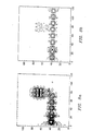
- Fig. 4 illustrates a two-dimensional stub-tuned photonic crystal waveguide apparatus according to an embodiment of the invention.
- the apparatus is generally designated by reference number 40, and comprises a two-dimensional photonic crystal slab 42 having a waveguide 44 extending therethrough and created by omitting a single line of rods 46 of the array as described above with reference to Fig. 2.
- the photonic crystal slab 42 includes a resonant stub 47 (shown in dashed line) which extends from a sidewall of the waveguide 44 to control light in the waveguide.
- the resonant stub 47 includes a resonator region 48 and a connecting channel 50.
- connecting channel 50 comprises a short channel that extends from a sidewall of the waveguide 44 in a direction perpendicular to the waveguide; and is created by omitting two posts 46 from the array of posts.
- the resonator region 48 comprises a generally square region having a 3 x 3 sub-array of posts 52 which are larger in diameter than the posts 46.
- the connecting channel 50 comprises a short waveguide section which connects the resonator region 48 and the waveguide 44.
- the operation of the photonic crystal stub-tuned waveguide apparatus of Fig. 4 can best be explained by describing a simulation that was conducted.
- the radius of the posts 46 of the array is the same as in the simulation described with reference to Fig. 2, i.e., 0.18a o
- the waveguide 44 was created, as before, by omitting a row of the posts.
- the connecting channel 50 was created by omitting two of the posts 46 to define a short connecting channel 50 extending perpendicular to the waveguide 44.
- the resonator region 48 was created by providing a 3 x 3 sub-array of posts 52, each of which had a radius of 0.25a o .
- Fig. 5 is a graph similar to that of Fig. 3 and illustrates the results of the simulation conducted using the apparatus of Fig. 4 having the parameters described above. Results of the simulation show that the waveguide transmission characteristics of the waveguide apparatus of Fig. 2 were modified by a sharp transmission zero illustrated by the dashed line in Fig. 5.
- This transmission zero is a narrow range of frequencies within the bandgap of the photonic crystal material at which light that is otherwise capable of propagating through the waveguide 44 (as is shown in Fig. 3), is prevented from propagating through the waveguide.
- the frequency of the transmission zero corresponds to a resonant frequency of the 3 x 3 resonator region 48, while properties of the connecting channel control the coupling between the resonator region and the waveguide 44.
- the coupling controls the quality factor (Q-factor) of the resonator region; and, thus, the bandwidth of the transmission zero.
- the stub has very little interaction with the propagating waveguide mode for frequencies away from the transmission zero, as shown in Fig. 6a.
- the resonator region of the stub contains a great deal of electromagnetic energy. This energy leaks back into the waveguide with a magnitude and phase that cause a full reflection of the incident light, as shown in Fig. 6b.
- the photonic crystal stub-tuned waveguide apparatus 40 of Fig. 4 provides a great deal of design flexibility for controlling light in the waveguide 44.
- the resonant frequency of the resonator region can be controlled; and this, in turn, controls the frequency of the transmission zero.
- the connecting channel controls the coupling between the resonator region and the waveguide. This, in turn, controls the quality factor of the resonant region and thus the bandwidth of the transmission zero.
- the resonator region parameters that can be controlled include, for example, the number of posts comprising the region and the diameter of the posts, both of which will contribute to defining the resonance frequency.
- Connecting channel parameters that can be controlled include, for example, the length and width of the channel, the number of posts omitted from the channel, and the number of posts and the diameter of posts included in the channel (in embodiments in which posts are included in the connecting channel).
- a tuner in addition to controlling design parameters of the resonant stub of the waveguide apparatus to control transmission characteristics of the waveguide; a tuner is additionally provided to control properties of the transmission zero by tuning parameters of the resonant modes of the stub.
- the tuner which is schematically illustrated in Fig. 4 by reference number 49, comprises a dielectric constant tuner for tuning the dielectric constant of the material comprising the posts in the resonator region.
- dielectric constant tuners are well-known to those skilled in the art, and thus need not be described in any detail herein, and can be either electronic or optical.
- an electronic dielectric constant tuner may utilize the charge carrier effect or the electro-optic effect.
- An optical dielectric constant tuner may utilize the photorefractive effect. Although all of these effects are relatively small in the optical frequency regime, they appear large enough to effect appropriate tuning of the apparatus of the present invention.
- Fig. 7 is a plot illustrating the waveguide transmission for incident light at a fixed frequency corresponding to the frequency of the transmission zero of the "untuned" stub waveguide apparatus of Fig. 4, computed as a function of the effective dielectric constant of the posts in the resonator region. Note that when the posts of the resonator region have the nominal dielectric value of 11.4, the waveguide transmission is effectively zero. As the dielectric constant of the resonator region posts is tuned by only a few percent, the waveguide transmission approaches the full value calculated for the photonic crystal waveguide without a tuner as is shown in Fig. 3. Figs.
- 8a and 8b are contour plots of the computed field magnitudes for the nominal-zero transmission case and for the case where the dielectric constant of the resonator region has been increased by 4%, respectively.
- the illustrated behavior clearly corresponds to the operation of an on/off optical switch as the dielectric constant is switched from one to another value through the full range plotted.
- the described behavior also clearly corresponds to the operation of an optical modulator as the dielectric constant is tuned through intermediate values.
- the simulated performance described above is intended to be exemplary only, as operational characteristics of the apparatus of the present invention can be modified in many ways. For example, by reducing the coupling between the waveguide and the resonator region through modification of the connecting channel; the width of the zero notch shown in Fig. 5 can be reduced, leading to enhanced sensitivity to the dielectric constant tuning of the resonator region posts. This will permit switching to be achieved with much smaller changes in the dielectric constant, but with a reduced frequency tuning range. All of the methods described herein for modifying specific operational characteristics of the photonic crystal waveguide apparatus of the invention, as well as other methods, will be readily apparent to those skilled in the art; and it is not intended to limit the invention in this regard.
- the photonic crystal lattice structure incorporated in the previously described two-dimensional structures can take a number of three-dimensional realizations.
- Two exemplary three-dimensional geometries are shown in Figs. 9a and 9b, making explicit the finite length of the dielectric posts.
- post units comprising photonic crystal post portions 62 are sandwiched between upper and lower cladding layer post portions 64 and 66, with each post unit being supported on a substrate 68.
- the structure 70 shown in Fig. 9b lacks the upper cladding post portions 64.
- optical confinement in the dimension parallel to the posts is effected by the larger dielectric constant of the photonic crystal region, leading to total internal reflection of the light in this dimension. It should also be noted that another realization could be to have the posts of the photonic crystal "sandwiched" between two reflective surfaces, either dielectric or metallic, to provide the confinement necessary in the dimension parallel to the posts.
- the photonic crystal waveguide apparatus described above generally comprise arrays of dielectric rods in air; the photonic crystals can also be composed of an array of gas or vacuum "filled" holes in a dielectric substrate, or an array of dielectric rods embedded in a body of a dielectric material having a different dielectric constant than that of the material of the rods.
- the above embodiments generally describe two-dimensional apparatus; the invention can also be applied to fully three-dimensional photonic crystal apparatus with the same sort of operational characteristics.
- the photonic crystal waveguide apparatus of the present invention operates as a tunable notch filter, where the action of the resonator is as a purely reflective agent causing the propagation characteristic of the waveguide to have a transmission zero at a specified, tunable frequency.
- the apparatus can be employed as an on/off optical switch and as an optical modulator, as described above; and, in general, can be used in any application where a tunable optical filter would be useful, with one example being as a channel drop filter.
- the tuning agent can be either electronically or optically activated.
- the invention can take many other forms.
- the embodiments described herein include a single resonant stub extending from the waveguide, in other embodiments, two or more resonant stubs may be provided.
- two or more resonant stubs having resonator regions and/or connecting channels with different parameters, and sufficiently spaced from one another so as to not interfere, two or more transmission zeros can be created in the bandgap of the photonic crystal.
Landscapes
- Physics & Mathematics (AREA)
- Optics & Photonics (AREA)
- Engineering & Computer Science (AREA)
- Nanotechnology (AREA)
- Chemical & Material Sciences (AREA)
- General Physics & Mathematics (AREA)
- Life Sciences & Earth Sciences (AREA)
- Crystallography & Structural Chemistry (AREA)
- Biophysics (AREA)
- Microelectronics & Electronic Packaging (AREA)
- Electromagnetism (AREA)
- Nonlinear Science (AREA)
- Optical Integrated Circuits (AREA)
- Optical Modulation, Optical Deflection, Nonlinear Optics, Optical Demodulation, Optical Logic Elements (AREA)
Applications Claiming Priority (2)
| Application Number | Priority Date | Filing Date | Title |
|---|---|---|---|
| US09/846,856 US6687447B2 (en) | 2001-04-30 | 2001-04-30 | Stub-tuned photonic crystal waveguide |
| US846856 | 2001-04-30 |
Publications (2)
| Publication Number | Publication Date |
|---|---|
| EP1255136A2 true EP1255136A2 (fr) | 2002-11-06 |
| EP1255136A3 EP1255136A3 (fr) | 2003-02-26 |
Family
ID=25299132
Family Applications (1)
| Application Number | Title | Priority Date | Filing Date |
|---|---|---|---|
| EP02002176A Ceased EP1255136A3 (fr) | 2001-04-30 | 2002-01-29 | Guide d'onde optique à cristal photonique réglable par un bras résonnant |
Country Status (3)
| Country | Link |
|---|---|
| US (1) | US6687447B2 (fr) |
| EP (1) | EP1255136A3 (fr) |
| JP (1) | JP4084075B2 (fr) |
Cited By (6)
| Publication number | Priority date | Publication date | Assignee | Title |
|---|---|---|---|---|
| WO2003065113A1 (fr) * | 2002-01-28 | 2003-08-07 | The Board Of Trustees Of The Leland Stanford Junior University | Creation de formes lineaires asymetriques aigues dans des structures de microcavite |
| EP1403684A1 (fr) * | 2002-09-30 | 2004-03-31 | Corning Incorporated | Modulateur optique à grande vitesse |
| WO2004027470A1 (fr) * | 2002-09-19 | 2004-04-01 | The University Of Bristol | Filtre |
| DE102004050176A1 (de) * | 2004-09-20 | 2006-03-23 | Universität Duisburg-Essen | Optoelektronisches Bauelement und Verfahren zum Steuern von Tunnelelektronenströmen durch Photonen |
| EP1975983A2 (fr) | 2003-07-14 | 2008-10-01 | Nikon Corporation | Système optique de collecteur, unité de source lumineuse, appareil optique d'éclairage, et appareil d'exposition |
| CN100444016C (zh) * | 2004-05-24 | 2008-12-17 | 中国科学院光电技术研究所 | 光子晶体变频装置 |
Families Citing this family (26)
| Publication number | Priority date | Publication date | Assignee | Title |
|---|---|---|---|---|
| CA2350352A1 (fr) * | 2001-06-13 | 2002-12-13 | Linda P.B. Katehi | Filtres planaires faisant appel a des substrats periodiques a bande interdite electromagnetique |
| US6760514B2 (en) * | 2002-02-27 | 2004-07-06 | Agilent Technologies, Inc. | Continuously tunable photonic crystal drop filter |
| JP3721142B2 (ja) * | 2002-03-26 | 2005-11-30 | 独立行政法人科学技術振興機構 | 2次元フォトニック結晶点欠陥干渉光共振器及び光反射器 |
| US6947649B2 (en) * | 2002-05-31 | 2005-09-20 | Matsushita Electric Industrial Co., Ltd. | Method of adjusting the index of refraction of photonic crystals with laser micromachining to tune transmissions within the bandgap and structure |
| US6728457B2 (en) * | 2002-07-10 | 2004-04-27 | Agilent Technologies, Inc. | Waveguides in two dimensional slab photonic crystals with noncircular holes |
| US7026640B2 (en) * | 2002-08-02 | 2006-04-11 | Ramot At Tel Aviv University Ltd. | Method and systems for dynamically controlling electromagnetic wave motion through a photonic crystal |
| JP3682289B2 (ja) * | 2002-12-06 | 2005-08-10 | 独立行政法人科学技術振興機構 | 境界反射を利用した2次元フォトニック結晶光分合波器 |
| JP4171326B2 (ja) | 2003-03-17 | 2008-10-22 | 国立大学法人京都大学 | 2次元フォトニック結晶中の共振器と波長分合波器 |
| WO2005071451A1 (fr) * | 2004-01-22 | 2005-08-04 | Matsushita Electric Industrial Co., Ltd. | Dispositif optique et procede de fabrication d'une plaque de cristal photonique |
| CN1325947C (zh) * | 2004-02-03 | 2007-07-11 | 复旦大学 | 一种调节光子晶体禁带位置的方法 |
| DE602005016330D1 (de) * | 2004-03-30 | 2009-10-15 | Canon Kk | Anzeigevorrichtung, Bildbetrachtungsvorrichtung und Projektionsanordnung unter Verwendung desselben |
| US6993234B1 (en) * | 2004-08-03 | 2006-01-31 | Agilent Technologies, Inc. | Photonic crystal resonator apparatus with improved out of plane coupling |
| US7609376B2 (en) * | 2005-01-05 | 2009-10-27 | Hewlett-Packard Development Company, L.P. | Method and apparatus for pixel display and SERS analysis |
| US7228042B2 (en) * | 2005-03-04 | 2007-06-05 | International Business Machines Corporation | Method and apparatus for resonant coupling in photonic crystal circuits |
| JPWO2009087825A1 (ja) * | 2008-01-11 | 2011-05-26 | 日本電気株式会社 | フォトニック結晶体 |
| US8050173B2 (en) * | 2008-07-01 | 2011-11-01 | Broadcom Corporation | Dynamic precision for datapath modules |
| US8189968B2 (en) * | 2008-08-28 | 2012-05-29 | Board Of Regents, The University Of Texas | Multimode interference coupler for use with slot photonic crystal waveguides |
| US8477402B2 (en) | 2010-09-20 | 2013-07-02 | The Invention Science Fund I Llc | Photonic modulation of a photonic band gap |
| USD758372S1 (en) | 2013-03-13 | 2016-06-07 | Nagrastar Llc | Smart card interface |
| US9888283B2 (en) | 2013-03-13 | 2018-02-06 | Nagrastar Llc | Systems and methods for performing transport I/O |
| USD864968S1 (en) | 2015-04-30 | 2019-10-29 | Echostar Technologies L.L.C. | Smart card interface |
| US11690160B2 (en) * | 2019-09-10 | 2023-06-27 | The Board Of Trustees Of The University Of Illinois | Plasma photonic crystals with integrated plasmonic arrays in a microtubular frame |
| CN116243506A (zh) * | 2022-12-15 | 2023-06-09 | 珠海光库科技股份有限公司 | 一种基于二维拓扑光子晶体的电光调制器芯片 |
| DE102023211699A1 (de) * | 2023-11-23 | 2025-05-28 | Continental Autonomous Mobility Germany GmbH | Wellenleiteranordnung sowie Radarsensor |
| US20250300356A1 (en) * | 2024-03-20 | 2025-09-25 | Lockheed Martin Corporation | Horn Antennas With Integrated Feeds |
| CN118920055A (zh) * | 2024-07-22 | 2024-11-08 | 电子科技大学 | 一种光子晶体加载的非接触式w波段矩形波导连接结构 |
Family Cites Families (6)
| Publication number | Priority date | Publication date | Assignee | Title |
|---|---|---|---|---|
| US4550330A (en) | 1984-06-29 | 1985-10-29 | International Business Machines Corporation | Semiconductor interferometer |
| US6058127A (en) | 1996-12-13 | 2000-05-02 | Massachusetts Institute Of Technology | Tunable microcavity and method of using nonlinear materials in a photonic crystal |
| US6101300A (en) | 1997-06-09 | 2000-08-08 | Massachusetts Institute Of Technology | High efficiency channel drop filter with absorption induced on/off switching and modulation |
| US5999308A (en) * | 1998-04-01 | 1999-12-07 | Massachusetts Institute Of Technology | Methods and systems for introducing electromagnetic radiation into photonic crystals |
| US6198860B1 (en) * | 1998-09-22 | 2001-03-06 | Massachusetts Institute Of Technology | Optical waveguide crossings |
| US6175671B1 (en) * | 1998-10-01 | 2001-01-16 | Nortel Networks Limited | Photonic crystal waveguide arrays |
-
2001
- 2001-04-30 US US09/846,856 patent/US6687447B2/en not_active Expired - Fee Related
-
2002
- 2002-01-29 EP EP02002176A patent/EP1255136A3/fr not_active Ceased
- 2002-04-19 JP JP2002116966A patent/JP4084075B2/ja not_active Expired - Fee Related
Cited By (8)
| Publication number | Priority date | Publication date | Assignee | Title |
|---|---|---|---|---|
| WO2003065113A1 (fr) * | 2002-01-28 | 2003-08-07 | The Board Of Trustees Of The Leland Stanford Junior University | Creation de formes lineaires asymetriques aigues dans des structures de microcavite |
| US6819691B2 (en) | 2002-01-28 | 2004-11-16 | The Board Of Trustees Of The Leland Stanford Junior University | Creating sharp asymmetric lineshapes in microcavity structures |
| WO2004027470A1 (fr) * | 2002-09-19 | 2004-04-01 | The University Of Bristol | Filtre |
| EP1403684A1 (fr) * | 2002-09-30 | 2004-03-31 | Corning Incorporated | Modulateur optique à grande vitesse |
| EP1975983A2 (fr) | 2003-07-14 | 2008-10-01 | Nikon Corporation | Système optique de collecteur, unité de source lumineuse, appareil optique d'éclairage, et appareil d'exposition |
| CN100444016C (zh) * | 2004-05-24 | 2008-12-17 | 中国科学院光电技术研究所 | 光子晶体变频装置 |
| DE102004050176A1 (de) * | 2004-09-20 | 2006-03-23 | Universität Duisburg-Essen | Optoelektronisches Bauelement und Verfahren zum Steuern von Tunnelelektronenströmen durch Photonen |
| US7421177B2 (en) | 2004-09-20 | 2008-09-02 | Universitat Duisburg-Essen | Optoelectronic component and method for controlling tunneling electron currents by means of photons |
Also Published As
| Publication number | Publication date |
|---|---|
| US20020159733A1 (en) | 2002-10-31 |
| JP2002365599A (ja) | 2002-12-18 |
| JP4084075B2 (ja) | 2008-04-30 |
| US6687447B2 (en) | 2004-02-03 |
| EP1255136A3 (fr) | 2003-02-26 |
Similar Documents
| Publication | Publication Date | Title |
|---|---|---|
| US6687447B2 (en) | Stub-tuned photonic crystal waveguide | |
| JP4380957B2 (ja) | 集積光スイッチングデバイスおよび光をスイッチングする方法 | |
| CA2293660C (fr) | Filtre de transfert de canaux a haute efficacite a commutation et modulation commandees par l'absorption | |
| US6873777B2 (en) | Two-dimensional photonic crystal device | |
| US6674949B2 (en) | Active photonic crystal waveguide device and method | |
| US6130969A (en) | High efficiency channel drop filter | |
| JP2002303836A (ja) | フォトニック結晶構造を有する光スイッチ | |
| WO2000017679A9 (fr) | Croisements de guides d'ondes optiques | |
| JP2004245866A (ja) | 2次元フォトニック結晶中の共振器と波長分合波器 | |
| US6760514B2 (en) | Continuously tunable photonic crystal drop filter | |
| WO2009087825A1 (fr) | Élément à cristal photonique | |
| EP1296177B1 (fr) | Commutateur ou modulateur interferométrique comprenant des guides d'onde à cristal photonique | |
| US7428348B2 (en) | Electro-optical switching using coupled photonic crystal waveguides | |
| JP2004279800A (ja) | 2次元フォトニック結晶中の共振器と波長分合波器 | |
| JP2006323090A (ja) | 3次元フォトニック結晶およびそれを用いた光学素子 | |
| JPWO2010073704A1 (ja) | 光スイッチ | |
| US6735235B2 (en) | Three-dimensional photonic crystal add-drop filter | |
| US6993234B1 (en) | Photonic crystal resonator apparatus with improved out of plane coupling | |
| Shinya et al. | Ultrasmall resonant tunneling/dropping devices in 2D photonic crystal slabs | |
| Shinya et al. | Functional devices in photonic crystals for future photonic integrated circuits | |
| Kelmelis et al. | Design and implementation of novel photonic crystal tunable devices |
Legal Events
| Date | Code | Title | Description |
|---|---|---|---|
| PUAI | Public reference made under article 153(3) epc to a published international application that has entered the european phase |
Free format text: ORIGINAL CODE: 0009012 |
|
| AK | Designated contracting states |
Kind code of ref document: A2 Designated state(s): AT BE CH CY DE DK ES FI FR GB GR IE IT LI LU MC NL PT SE TR |
|
| AX | Request for extension of the european patent |
Free format text: AL;LT;LV;MK;RO;SI |
|
| PUAL | Search report despatched |
Free format text: ORIGINAL CODE: 0009013 |
|
| RIC1 | Information provided on ipc code assigned before grant |
Ipc: 7H 01P 1/20 B Ipc: 7G 02F 1/01 B Ipc: 7G 02B 6/124 B Ipc: 7G 02B 6/122 A |
|
| AK | Designated contracting states |
Kind code of ref document: A3 Designated state(s): AT BE CH CY DE DK ES FI FR GB GR IE IT LI LU MC NL PT SE TR Designated state(s): AT BE CH CY DE DK ES FI FR GB GR IE IT LI LU MC NL PT SE TR |
|
| AX | Request for extension of the european patent |
Extension state: AL LT LV MK RO SI |
|
| 17P | Request for examination filed |
Effective date: 20030515 |
|
| 17Q | First examination report despatched |
Effective date: 20030722 |
|
| AKX | Designation fees paid |
Designated state(s): DE FR GB |
|
| APBN | Date of receipt of notice of appeal recorded |
Free format text: ORIGINAL CODE: EPIDOSNNOA2E |
|
| APBR | Date of receipt of statement of grounds of appeal recorded |
Free format text: ORIGINAL CODE: EPIDOSNNOA3E |
|
| APAA | Appeal reference recorded |
Free format text: ORIGINAL CODE: EPIDOS REFN |
|
| APAF | Appeal reference modified |
Free format text: ORIGINAL CODE: EPIDOSCREFNE |
|
| RAP1 | Party data changed (applicant data changed or rights of an application transferred) |
Owner name: AVAGO TECHNOLOGIES GENERAL IP (SINGAPORE) PTE. LTD |
|
| APBT | Appeal procedure closed |
Free format text: ORIGINAL CODE: EPIDOSNNOA9E |
|
| STAA | Information on the status of an ep patent application or granted ep patent |
Free format text: STATUS: THE APPLICATION HAS BEEN REFUSED |
|
| 18R | Application refused |
Effective date: 20070923 |