EP1255349A2 - Tiefpassfilter für den Ausgang eines Klasse - D Verstärkers - Google Patents
Tiefpassfilter für den Ausgang eines Klasse - D Verstärkers Download PDFInfo
- Publication number
- EP1255349A2 EP1255349A2 EP02252984A EP02252984A EP1255349A2 EP 1255349 A2 EP1255349 A2 EP 1255349A2 EP 02252984 A EP02252984 A EP 02252984A EP 02252984 A EP02252984 A EP 02252984A EP 1255349 A2 EP1255349 A2 EP 1255349A2
- Authority
- EP
- European Patent Office
- Prior art keywords
- inductors
- low pass
- pair
- pass filter
- inductor
- Prior art date
- Legal status (The legal status is an assumption and is not a legal conclusion. Google has not performed a legal analysis and makes no representation as to the accuracy of the status listed.)
- Granted
Links
Images


Classifications
-
- H—ELECTRICITY
- H03—ELECTRONIC CIRCUITRY
- H03F—AMPLIFIERS
- H03F3/00—Amplifiers with only discharge tubes or only semiconductor devices as amplifying elements
- H03F3/20—Power amplifiers, e.g. Class B amplifiers, Class C amplifiers
- H03F3/21—Power amplifiers, e.g. Class B amplifiers, Class C amplifiers with semiconductor devices only
- H03F3/217—Class D power amplifiers; Switching amplifiers
-
- H—ELECTRICITY
- H03—ELECTRONIC CIRCUITRY
- H03H—IMPEDANCE NETWORKS, e.g. RESONANT CIRCUITS; RESONATORS
- H03H7/00—Multiple-port networks comprising only passive electrical elements as network components
- H03H7/01—Frequency selective two-port networks
- H03H7/0115—Frequency selective two-port networks comprising only inductors and capacitors
Definitions
- the invention relates to a low pass filter for the removal of harmonics, which is connected to an output stage of a D-class amplifier having a plurality of channels.
- the D-class amplification is an amplifying scheme in which a modulating process such as pulse width modulation (PWM) or pulse density modulation (PDM) is performed to an analog signal supplied to an amplifying circuit, the processed analog signal is converted into a digital signal, thereafter, the digital signal is amplified, harmonics in an output are removed by a low pass filter, and the digital signal is returned to the analog signal.
- PWM pulse width modulation
- PDM pulse density modulation
- a low pass filter for an output stage of the D-class amplifier it is general to use a low pass filter of the so called LC type which comprises an inductor and a capacitor and of which an electric power loss is small.
- LC type which comprises an inductor and a capacitor and of which an electric power loss is small.
- miniaturize the low pass filter used at the output stage so that circuit elements arrangement on a printed circuit board can be integrated. This is because the high electric power efficiency and the miniaturization can be accomplished with a D-class amplifier, as mentioned above.
- coils obtained by winding conductors are generally used as inductors which are used for the low pass filter, however, if a load current flows in the inductors included in the low pass filter provided for one channel output, a change in magnetic flux occurs. When the magnetic flux is interlinked with inductors included in a low pass filter of another channel, an induced electromotive force is caused in the other inductor due to an electromagnetic induction phenomenon.
- the low pass filters at the output stage of the D-class amplifier having a plurality of output channels are integrated on a printed circuit board and arranged closely, interlinkage of the leakage magnetic flux from the inductor or inductors in the low pass filter of the adjacent channel may occur in the inductor or inductors of the low pass filter of the other channel. In that case, the leakage of the signal occurs between channels, and the separation between channels eventually deteriorates.
- the invention has been made to solve the points mentioned above and it is an object of the invention to provide a small low pass filter for output of a multichannel D-class amplifier in which prevention of the magnetic saturation of the inductor is sought while maintaining the separation between adjacent channels preferably.
- a low pass filter for output in a D-class amplifier having two or more signal amplifying channels, wherein each of the signal amplifying channels includes an even number of inductors, the low pass filter includes a first pair of inductors comprising inductors which are included in one of the signal amplifying channels and arranged so as to be adjacent to each other and an electrical connection is made, and a second pair of inductors comprising inductors which are included in one signal amplifying channel arranged in parallel so as to be adjacent to the one of signal amplifying channels and which are arranged so as to be adjacent to each other and connected, induced electromotive forces which are caused in the second pair of inductors by a leakage magnetic flux from the first pair of inductors are set off between the inductors included in the second pair of inductors, and induced electromotive forces which are caused in the first pair of inductors by a leakage magnetic flux from the second pair of inductors are set off between the inductors included in the first pair of in
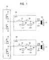
- Fig. 1 is a circuit diagram showing a construction of a low pass filter for output of a D-class amplifier according to the invention.
- a D-class amplifier IC (10) is, for example, a power amplifying IC having therein D-class amplifiers of a plurality of channels which construct an output stage circuit by an MOS-FET, and an output at the final stage is connected to the low pass filter for output every channel.
- the number of output channels of the multichannel D-class amplifier is set to, for example, 2 channels like a general stereophonic apparatus in the embodiment, the invention is not limited to it but it is sufficient to use the multichannel D-class amplifier having a plurality of channels of two or more.
- those channels are referred to as a channel 1 (hereinafter, referred to as CH1) and a channel 2 (hereinafter, referred to as CH2), and it is presumed that constructions and contents of those channels are substantially the same.
- a low pass filter 1 (20) (hereinafter, simply referred to as LPF1) is a low pass filter connected to an output of CH1 of the D-class amplifier IC (10) and is an LC type filter whose signal transfer function shows, for example, Butterworth characteristics or Chebyshev characteristics.
- the transfer function can be realized by using inductors as serial elements and using capacitors as parallel elements and sequentially cascade connecting those elements in a ladder form as shown in the circuit diagram of Fig. 1. Since the LPF1 exhibits large attenuating characteristics in a range of a predetermined frequency determined by the transfer function or higher, harmonic components of signal frequencies included in an output signal of CH1 can be sufficiently suppressed.
- L1 and L2 (23) (hereinafter, simply referred to as L1 and L2) constructing the LPF1
- L1 and L2 coils wound around bobbins or simple air-core coils can be used.
- Coils each having a core made of ferrite or another magnetic material can be also used.
- a black dot added to the side of each inductor indicates the start of winding of the coil constructing the inductor, as will be explained hereinlater.
- a capacitor C1 (22) and a capacitor C2 (24) are capacitors such as ceramic capacitors or laminated type Mylar capacitors and function so as to realize the attenuating characteristics by the transfer function of the LPF1 together with the inductors.
- the order of the LPF1, that is, the number of inductors and capacitors included in the low pass filter is not limited to the number shown in the embodiment but determined in accordance with harmonic suppressing characteristics which are necessary as a low pass filter for output of the D-class amplifier.
- a condition that the number of inductors included in the low pass filter is an even number is assumed to be a necessary condition.
- the low pass filter in the embodiment has a construction of the forth order, that is, it has two inductors.
- Each speaker (40) converts an output electric signal from the LPF1 into an acoustic signal and generates it as a sound.
- a low pass filter 2 (30) (hereinafter, simply referred to as LPF2) is a low pass filter connected to an output of CH2 of the D-class amplifier and constructed by an inductor L3 (31), an inductor L4 (33), a capacitor C3 (32), and a capacitor C4 (34) (hereinafter, simply referred to as L3, L4, C3, and C4, respectively). Since a circuit construction and each component element of the LPF2 are substantially the same as those of the LPF1, their descriptions are omitted here.
- circuit constructions, component elements, and circuit constants of the LPF1 and LPF2 are substantially the same. Subsequently, a physical arrangement of the component elements of the LPFs on a printed circuit board will be described.
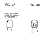
- An inductor has an external view having a cylindrical inductor casing as shown in Fig. 3A and its inside is constructed by a coil wound like a cylinder around a bobbin as shown in Fig. 3B. As shown in Fig. 3A, a mark indicative of the start of the winding of the coil is written onto an upper surface portion of the inductor casing. Whether a terminal to supply a current to the inductor is set to an A side or a B side shown in the diagram is determined by using the mark as a reference point, and the inductor can be arranged.
- each inductor is implemented onto the printed circuit board in the direction such that a diameter of the cylindrical coil is parallel with the printed circuit board.
- a center axis of the coil and the generating direction of a magnetic flux are, therefore, perpendicular to the printed circuit board.
- the circuit constructions, component elements, and circuit constants of the LPFs included in CH1 and CH2 are substantially the same.
- the two inductors which are included in the LPF1 of CH1 and connected so as to be adjacent to each other are set to a first pair of inductors, also in the LPF2 of CH2, a second pair of inductors arranged at the same positions also on the circuit diagram as those of the first pair of inductors exist in correspondence to the first pair of inductors. That is, assuming that L1 and L2 included in the LPF1 of CH1 are the first pair of inductors, L3 and L4 included in the LPF2 of CH2 are the second pair of inductors.
- L1 to L4 included in the LPF1 and LPF2 are arranged on the printed circuit board in a manner such that they are located at vertexes of a rectangular parallelogram on the printed circuit board.
- Distances between the corresponding inductors with respect to the inductor pairs of the LPF1 and LPF2 therefore, that is, a distance between the center axes of the coils of L1 and L3 and that of L2 and L4 are equal.
- Distances between the inductors of a different correspondence relation with respect to the two inductor pairs that is, a distance between the center axes of the coils of L1 and L4 and that of L2 and L3 are also equal.
- a mutual inductance M between the two inductors is unconditionally determined only by the physical arrangements of both inductors irrespective of load currents or voltages of the inductors.
- a mutual inductance between L1 and L3 is, therefore, determined as M13.
- a mutual inductance between L2 and L4 is assumed to be M24, that between L1 and L4 is assumed to be M14, and that between L2 and L3 is assumed to be M23, respectively.
- the following relational equations are satisfied among the mutual inductance between the respective inductors arranged as shown in Figs. 2A and 2B.
- M13 M24
- M14 M23
- a mutual inductance M31 is a mutual inductance at the time when an induced electromotive force e31 which is caused in L3 of the LPF2 is defined by a load current i1 flowing in L1 of the LPF1 and defined by the following relational equation by the rule of electromagnetic induction.
- e31 -M31 ⁇ (di1/dt)
- the D-class amplifier IC (10) is shown as a mere voltage source and the speakers (40) are also shown as mere load resistors. Since the capacitors in the LPF1 and LPF2 are not much concerned with the essential operation in the embodiment, their descriptions are omitted here.
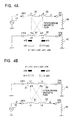
- Fig. 4A is a diagram for explaining an electromotive force which is induced in each inductor included in the LPF2 when the load current i1 flows in the LPF1.
- the load current i1 flows in L1 and L2 of the LPF1
- a change in magnetic flux occurs.
- the magnetic flux is interlinked with L3 and L4 of the LPF2, induced electromotive forces are generated in L3 and L4.
- induced electromotive forces that are generated in L3 and L4 by the magnetic flux from L1 are now assumed to be e31 and e41, and similarly, induced electromotive forces that are generated in L3 and L4 by the magnetic flux from L2 are assumed to be e32 and e42, respectively.
- the positions of the black dot marks indicative of the winding directions with respect to L1-L3 and L2-L3 coincide. That is, with respect to those inductors, their winding directions are the same.
- L2-L4 and L1-L4 the positions of the black dot marks are different and the winding directions regarding the respective inductors are opposite.
- the winding directions of the two inductors arranged in a manner such that the center axes of the coils are located on parallel lines coincide, by the current flowing in one inductor, the direction of the electromotive force which is induced in the other inductor is the same as that of the current flowing in the original inductor. If the winding directions of the inductors are opposite, by the current flowing in one inductor, the direction of the electromotive force which is induced in the other inductor is opposite to that of the current flowing in the original inductor. This phenomenon is derived from the rule of the electromagnetic induction.
- the induced electromotive force e in the circuit of Fig. 4A can be expressed by the following equation also in consideration of the directions.
- the directions of the induced electromotive forces e31 and e32 which are caused in the same direction as that of the load current i1 flowing in the LPF1 are set to the positive direction.
- e e31 + e32 - e41 - e42
- a value of the induced electromotive force which is generated in each inductor can be expressed by the following equations by using the mutual inductance between the inductors.
- e31 -M31 ⁇ (di1/dt)
- e32 -M32 ⁇ (di1/dt)
- e41 -M41 ⁇ (di1/dt)
- e42 -M42 ⁇ (di1/dt)
- the electromotive forces which are generated in the inductors included in the LPF2 of CH2 by the load current i1 flowing in the LPF1 of CH1 are set off by the respective inductors, so that the sum e is equal to 0. In other words, a leakage of the signal from CH1 to CH2 is not caused apparently.
- FIG. 5 Another embodiment of the invention is shown in a circuit diagram of Fig. 5.
- the circuit of Fig. 5 shows the construction of the low pass filter circuit in the case where the output stage of the D-class amplifier uses the BTL (Balanced Tied Load) system.
- the BTL system is an output stage system of an amplifier in which loads are connected between output terminals of two SEPP (Single Ended Push-Pull) circuits of opposite phases.
- SEPP Single Ended Push-Pull
- the winding directions of the inductors included in the LPF1 connected between the two output stages of CH1 and the LPF2 of CH2 are set in a manner similar to those in the circuit shown in Fig. 1. It is assumed that the physical arrangements of the inductors on a printed circuit board of the circuit of Fig. 5 are similar to those in the cases of Figs. 2A and 2B with respect to the LPF1 and LPF2.
- the leakage magnetic flux that is caused from one channel does not exercise an influence to the other adjacent channel. Even if the leakage magnetic flux is caused between the channels, the separation between the channels is preferably held.
- the low pass filter for output of the D-class amplifier of the invention while the separation between the channels is preferably held, the low pass filter for output of a plurality of channels can be integrated and implemented onto the printed circuit board.
- the construction of the low pass filter for output of the multichannel D-class amplifier can be miniaturized.
Landscapes
- Engineering & Computer Science (AREA)
- Power Engineering (AREA)
- Amplifiers (AREA)
- Circuit For Audible Band Transducer (AREA)
- Filters And Equalizers (AREA)
Applications Claiming Priority (2)
| Application Number | Priority Date | Filing Date | Title |
|---|---|---|---|
| JP2001133920A JP2002330035A (ja) | 2001-05-01 | 2001-05-01 | D級アンプ出力用ローパスフィルタ |
| JP2001133920 | 2001-05-01 |
Publications (3)
| Publication Number | Publication Date |
|---|---|
| EP1255349A2 true EP1255349A2 (de) | 2002-11-06 |
| EP1255349A3 EP1255349A3 (de) | 2004-01-07 |
| EP1255349B1 EP1255349B1 (de) | 2004-11-10 |
Family
ID=18981698
Family Applications (1)
| Application Number | Title | Priority Date | Filing Date |
|---|---|---|---|
| EP02252984A Expired - Lifetime EP1255349B1 (de) | 2001-05-01 | 2002-04-26 | Tiefpassfilter für den Ausgang eines Klasse - D Verstärkers |
Country Status (4)
| Country | Link |
|---|---|
| US (1) | US6882222B2 (de) |
| EP (1) | EP1255349B1 (de) |
| JP (1) | JP2002330035A (de) |
| DE (1) | DE60201857T2 (de) |
Cited By (2)
| Publication number | Priority date | Publication date | Assignee | Title |
|---|---|---|---|---|
| WO2007078669A1 (en) * | 2005-12-19 | 2007-07-12 | Bose Corporation | Amplifier output filter having planar inductor |
| CN108215493A (zh) * | 2016-12-22 | 2018-06-29 | 精工爱普生株式会社 | 液体喷出装置以及电路基板 |
Families Citing this family (5)
| Publication number | Priority date | Publication date | Assignee | Title |
|---|---|---|---|---|
| US7157964B2 (en) * | 2003-08-11 | 2007-01-02 | Jam Technologies, Inc. | Multi-output switching amplifier |
| ATE417410T1 (de) * | 2004-11-25 | 2008-12-15 | Murata Manufacturing Co | Hochfrequenzschaltmodul |
| US7545208B2 (en) * | 2005-11-12 | 2009-06-09 | Manuel De Jesus Rodriguez | Signal amplification through an electromagnetic device |
| JP5077132B2 (ja) | 2008-08-06 | 2012-11-21 | ヤマハ株式会社 | 電力増幅器およびコモンモードチョークコイル |
| US20140333378A1 (en) * | 2013-05-08 | 2014-11-13 | Udo Karthaus | Circuit arrangement for generating a radio frequency signal |
Family Cites Families (3)
| Publication number | Priority date | Publication date | Assignee | Title |
|---|---|---|---|---|
| DE4007566C2 (de) * | 1990-03-09 | 1998-07-16 | Siemens Ag | Leistungsverstärker für die Speisung einer Induktivität mit geschalteten Transistoren |
| US5982231A (en) * | 1997-07-23 | 1999-11-09 | Linfinity Microelectronics, Inc. | Multiple channel class D audio amplifier |
| US6392476B1 (en) * | 2000-03-14 | 2002-05-21 | Harman International Industries, Incorporated | System and method of producing direct audio from a power supply |
-
2001
- 2001-05-01 JP JP2001133920A patent/JP2002330035A/ja not_active Abandoned
-
2002
- 2002-04-26 DE DE60201857T patent/DE60201857T2/de not_active Expired - Fee Related
- 2002-04-26 EP EP02252984A patent/EP1255349B1/de not_active Expired - Lifetime
- 2002-04-30 US US10/134,696 patent/US6882222B2/en not_active Expired - Fee Related
Cited By (3)
| Publication number | Priority date | Publication date | Assignee | Title |
|---|---|---|---|---|
| WO2007078669A1 (en) * | 2005-12-19 | 2007-07-12 | Bose Corporation | Amplifier output filter having planar inductor |
| US7432793B2 (en) | 2005-12-19 | 2008-10-07 | Bose Corporation | Amplifier output filter having planar inductor |
| CN108215493A (zh) * | 2016-12-22 | 2018-06-29 | 精工爱普生株式会社 | 液体喷出装置以及电路基板 |
Also Published As
| Publication number | Publication date |
|---|---|
| DE60201857D1 (de) | 2004-12-16 |
| US20020196078A1 (en) | 2002-12-26 |
| EP1255349A3 (de) | 2004-01-07 |
| DE60201857T2 (de) | 2005-10-20 |
| JP2002330035A (ja) | 2002-11-15 |
| EP1255349B1 (de) | 2004-11-10 |
| US6882222B2 (en) | 2005-04-19 |
Similar Documents
| Publication | Publication Date | Title |
|---|---|---|
| USRE42448E1 (en) | Switched-mode power amplifier integrally performing power combining | |
| KR101529779B1 (ko) | 스피커 코일을 통해 무선 주파수 신호를 전송하는 시스템 및 회로 | |
| US20050212619A1 (en) | Filter circuit | |
| EP1003295A3 (de) | Ein sättigungsfreies, flussunterdrückendes Diplexfilter für Netzleitungskommunikation | |
| JPH02177605A (ja) | パルス幅変調増幅回路 | |
| US20190260343A1 (en) | Lc filter | |
| WO2008097758A1 (en) | Hybrid filter for audio switching amplifier | |
| EP1255349B1 (de) | Tiefpassfilter für den Ausgang eines Klasse - D Verstärkers | |
| KR100673347B1 (ko) | 노이즈 억제 회로 | |
| US7199692B2 (en) | Noise suppressor | |
| EP1617704B1 (de) | Empfänger mit mehreren Antriebsspulen | |
| US3931469A (en) | Crossover network for a multi-element electrostatic loudspeaker system | |
| JP2831252B2 (ja) | E級プッシュプル電力増幅回路 | |
| CN101150303A (zh) | 用于电信系统中的xDSL分路器的多阶低通滤波器 | |
| US20200119709A1 (en) | Balun | |
| US11088669B2 (en) | Band pass filter | |
| CN1523755A (zh) | 噪声滤波器及使用该噪声滤波器的plc调制解调器 | |
| WO2015048704A2 (en) | Method and circuitry for multi-stage amplification | |
| JP2002057542A (ja) | 電力変換器用ラインフィルタ | |
| JP4067475B2 (ja) | 信号増幅出力装置 | |
| JPH0320057B2 (de) | ||
| CN223230178U (zh) | 主动式扼流圈 | |
| JP3925371B2 (ja) | 交流/直流分離回路 | |
| JPH09148144A (ja) | ノイズフィルタ用インダクタ | |
| JP2001285005A (ja) | ノイズフィルタ |
Legal Events
| Date | Code | Title | Description |
|---|---|---|---|
| PUAI | Public reference made under article 153(3) epc to a published international application that has entered the european phase |
Free format text: ORIGINAL CODE: 0009012 |
|
| AK | Designated contracting states |
Kind code of ref document: A2 Designated state(s): AT BE CH CY DE DK ES FI FR GB GR IE IT LI LU MC NL PT SE TR |
|
| AX | Request for extension of the european patent |
Free format text: AL;LT;LV;MK;RO;SI |
|
| PUAL | Search report despatched |
Free format text: ORIGINAL CODE: 0009013 |
|
| AK | Designated contracting states |
Kind code of ref document: A3 Designated state(s): AT BE CH CY DE DK ES FI FR GB GR IE IT LI LU MC NL PT SE TR |
|
| AX | Request for extension of the european patent |
Extension state: AL LT LV MK RO SI |
|
| GRAP | Despatch of communication of intention to grant a patent |
Free format text: ORIGINAL CODE: EPIDOSNIGR1 |
|
| 17P | Request for examination filed |
Effective date: 20040317 |
|
| GRAS | Grant fee paid |
Free format text: ORIGINAL CODE: EPIDOSNIGR3 |
|
| GRAA | (expected) grant |
Free format text: ORIGINAL CODE: 0009210 |
|
| AKX | Designation fees paid |
Designated state(s): DE FR GB |
|
| AK | Designated contracting states |
Kind code of ref document: B1 Designated state(s): DE FR GB |
|
| REG | Reference to a national code |
Ref country code: GB Ref legal event code: FG4D |
|
| REG | Reference to a national code |
Ref country code: IE Ref legal event code: FG4D |
|
| REF | Corresponds to: |
Ref document number: 60201857 Country of ref document: DE Date of ref document: 20041216 Kind code of ref document: P |
|
| PLBE | No opposition filed within time limit |
Free format text: ORIGINAL CODE: 0009261 |
|
| STAA | Information on the status of an ep patent application or granted ep patent |
Free format text: STATUS: NO OPPOSITION FILED WITHIN TIME LIMIT |
|
| ET | Fr: translation filed | ||
| 26N | No opposition filed |
Effective date: 20050811 |
|
| REG | Reference to a national code |
Ref country code: FR Ref legal event code: D6 |
|
| REG | Reference to a national code |
Ref country code: GB Ref legal event code: 746 Effective date: 20070308 |
|
| PGFP | Annual fee paid to national office [announced via postgrant information from national office to epo] |
Ref country code: DE Payment date: 20070419 Year of fee payment: 6 |
|
| PGFP | Annual fee paid to national office [announced via postgrant information from national office to epo] |
Ref country code: GB Payment date: 20070425 Year of fee payment: 6 |
|
| PGFP | Annual fee paid to national office [announced via postgrant information from national office to epo] |
Ref country code: FR Payment date: 20070411 Year of fee payment: 6 |
|
| GBPC | Gb: european patent ceased through non-payment of renewal fee |
Effective date: 20080426 |
|
| PG25 | Lapsed in a contracting state [announced via postgrant information from national office to epo] |
Ref country code: DE Free format text: LAPSE BECAUSE OF NON-PAYMENT OF DUE FEES Effective date: 20081101 |
|
| REG | Reference to a national code |
Ref country code: FR Ref legal event code: ST Effective date: 20081231 |
|
| PG25 | Lapsed in a contracting state [announced via postgrant information from national office to epo] |
Ref country code: FR Free format text: LAPSE BECAUSE OF NON-PAYMENT OF DUE FEES Effective date: 20080430 |
|
| PG25 | Lapsed in a contracting state [announced via postgrant information from national office to epo] |
Ref country code: GB Free format text: LAPSE BECAUSE OF NON-PAYMENT OF DUE FEES Effective date: 20080426 |