EP1260848A2 - Vorrichtung zur Ermittlung einer Lichtleistung, Mikroskop und Verfahren zur Mikroskopie - Google Patents
Vorrichtung zur Ermittlung einer Lichtleistung, Mikroskop und Verfahren zur Mikroskopie Download PDFInfo
- Publication number
- EP1260848A2 EP1260848A2 EP02100561A EP02100561A EP1260848A2 EP 1260848 A2 EP1260848 A2 EP 1260848A2 EP 02100561 A EP02100561 A EP 02100561A EP 02100561 A EP02100561 A EP 02100561A EP 1260848 A2 EP1260848 A2 EP 1260848A2
- Authority
- EP
- European Patent Office
- Prior art keywords
- light
- detector
- beam splitter
- microscope
- light output
- Prior art date
- Legal status (The legal status is an assumption and is not a legal conclusion. Google has not performed a legal analysis and makes no representation as to the accuracy of the status listed.)
- Granted
Links
Images


Classifications
-
- G—PHYSICS
- G02—OPTICS
- G02B—OPTICAL ELEMENTS, SYSTEMS OR APPARATUS
- G02B27/00—Optical systems or apparatus not provided for by any of the groups G02B1/00 - G02B26/00, G02B30/00
- G02B27/10—Beam splitting or combining systems
- G02B27/108—Beam splitting or combining systems for sampling a portion of a beam or combining a small beam in a larger one, e.g. wherein the area ratio or power ratio of the divided beams significantly differs from unity, without spectral selectivity
-
- G—PHYSICS
- G02—OPTICS
- G02B—OPTICAL ELEMENTS, SYSTEMS OR APPARATUS
- G02B21/00—Microscopes
-
- G—PHYSICS
- G02—OPTICS
- G02B—OPTICAL ELEMENTS, SYSTEMS OR APPARATUS
- G02B27/00—Optical systems or apparatus not provided for by any of the groups G02B1/00 - G02B26/00, G02B30/00
- G02B27/10—Beam splitting or combining systems
- G02B27/14—Beam splitting or combining systems operating by reflection only
- G02B27/144—Beam splitting or combining systems operating by reflection only using partially transparent surfaces without spectral selectivity
-
- G—PHYSICS
- G11—INFORMATION STORAGE
- G11B—INFORMATION STORAGE BASED ON RELATIVE MOVEMENT BETWEEN RECORD CARRIER AND TRANSDUCER
- G11B7/00—Recording or reproducing by optical means, e.g. recording using a thermal beam of optical radiation by modifying optical properties or the physical structure, reproducing using an optical beam at lower power by sensing optical properties; Record carriers therefor
Definitions
- the invention relates to a device for determining the light output of a Light beam with a beam splitter and one assigned to the beam splitter Detector.
- the invention relates to a microscope with a light source, the one Illuminating light beam emitted for illuminating a sample, with at least a detector device for detecting the emanating from the sample Detection light (61) and a device for determining the light output an illuminating light beam with a beam splitter and one Detector assigned to beam splitter
- the invention also relates to a method for microscopy.
- a sample In scanning microscopy, a sample is illuminated with a light beam the detection light emitted by the sample, as reflection or Fluorescent light, to observe.
- the focus of an illuminating light beam is generally controlled by means of a controllable beam deflection device Tilting two mirrors, moved in a sample plane, the Deflection axes are usually perpendicular to each other, so that a mirror in x, the other deflects in the y direction.
- the mirror will tilt accomplished, for example, with the help of galvanometer actuators.
- the power of the detection light coming from the object becomes dependent measured from the position of the scanning beam.
- the Control elements with sensors to determine the current mirror position equipped.
- a confocal Scanning microscope generally includes one light source, one Focusing optics, with which the light from the source onto a pinhole - the so-called Excitation diaphragm - is focused, a beam splitter, a Beam deflection device for beam control, microscope optics, a Detection aperture and the detectors for the detection of the detection or Fluorescent light.
- the illuminating light is through a beam splitter coupled.
- the fluorescent or reflection light coming from the object passes back to the beam splitter via the beam deflector, passes this, in order to then be focused on the detection aperture, behind which the detectors are located.
- This detection arrangement will Descan arrangement called. Detection light that is not directly from the Focus region originates, takes a different light path and passes through it Detection aperture is not, so that you get a point information by sequential scanning of the object with the focus of the Illumination light beam leads to a three-dimensional image. Usually a three-dimensional image is achieved by layered image data acquisition.
- Commercial scanning microscopes usually consist of a scanning module that is flanged to the stand of a classic light microscope, whereby the Scan module all necessary to scan a sample Includes elements.
- a well-known method, fluctuations and fluctuations in the Compensating or correcting illuminating light output is based on a measuring beam from the illuminating light beam with the aid of a beam splitter to divide and for image generation or image calculation the ratio of measured power of the measuring beam and detection light beam use.
- This procedure is for example in the publication G. J. Brakenhoff, Journal of Microscopy, Vol. 117, Pt 2, November 1979, p. 233-242.
- the invention is therefore based on the object of a device propose a largely accurate and reproducible determination enables the light output of a light beam.
- the invention has the advantage that a reliable measurement of the Light output of a light beam is made possible. Furthermore, the invention the advantage of a reliable, trouble-free and largely exact compensation of light output fluctuations, especially of Fluctuations in the illuminating light for illuminating a sample in the Microscopy and scanning microscopy.
- the light output of a light beam inter alia on interference can be traced back within the measuring light, even at the lowest mechanical or thermal disturbances to large fluctuations in the measured light output. Because of these disadvantages precise compensation of fluctuations in illuminating light output or stabilizing the illuminating light output in a microscope Set limits.
- the detector also receives the measurement light reduced spatial and / or temporal coherence.
- a scattering optical element such as a roughened glass plate or a frosted glass pane, provided.
- the beam splitter comprises a particularly preferred embodiment Substrate that has a diffusely scattering surface or at least partly consists of frosted glass.
- An embodiment variant in which the detector is particularly advantageous is arranged directly behind the beam splitter.
- This variant is particularly insensitive to external influences, insensitive to interference and compact. Often multiple reflections in the beam splitter result in multiple interference capable Partial beams, especially on the coated and uncoated Interfaces.
- the detector is therefore advantageously arranged in such a way that it is only from the primary divided measuring light, but not from others Partial light rays, is illuminated.
- the entrance window of the detector itself which is preferably is partially reflective coated as a beam splitter.
- the beam splitter consists of a Substrate that has a partially reflective coating.
- a partially reflective coating Preferably it is a metallic or dielectric coating.
- the coating is directly on the Detector or applied to the entrance window of the detector housing.
- the Beam splitter or the coating is preferred in one Design variant designed such that the ratio of Light outputs of the light beam to that measured at the detector Light output of the measuring light largely independent of the wavelength of the light beam is.
- the beam splitter (1) and the detector (11) combined into a unit that has a housing.
- An embodiment with a beam splitter is very particularly preferred, which generates a transmitted and a reflected partial beam and only the transmitted partial beam as a measuring beam on the detector meets.
- the reflected partial beam is applied to a sample as an illuminating light beam directed.
- the microscope is a scanning microscope or a confocal scanning microscope, which is preferably a processing unit that the measured power of the measuring light taking into account the Division ratio of the beam splitter and other system parameters with the Power of the detection light or a part, for example the power part of the detection light from a certain spectral range, charged.
- a processing unit is provided, the one programmable digital electronics, for example FPGA (Field Programmable Gate Arrray).
- A is preferably used to determine the power of the measurement light
- Semiconductor detector such as a photodiode or avalanche or PlN diode CCD chip or a photodetector provided because semiconductor detectors have a particularly small design. Also photomultiplier or Photomultiplier arrays can be used.
- Offsets are particularly important here Advantage, because with a pure relationship from detection light power The performance of the measuring light reduces even time constant offset portions not out. Offsets can come from the detectors, for example with incorrect zero adjustment or they can be caused by spreading or Ambient light, which inadvertently reaches the detectors, may be caused.
- the offsets are in a special embodiment of a Scan microscope automatically determined before scanning an image. For this purpose, the illuminating light is interrupted and that of the detectors outgoing signals measured and stored. With a Scaling step, which in the simplest case is multiplication by one Containing constants, the corrected light output is sent to any scale customizable.
- the method according to the invention comprises in the first two steps Determining a light output of an illuminating light beam with a Device comprising a beam splitter (1) and a beam splitter (1) assigned detector (11), the beam splitter (1) measuring light (23) split off from the illuminating light beam (37) and fed to the detector (11) and the ratio of the light output of the illuminating light beam (37) to that at the detector (11) measured light power of the measuring light (23) in time is constant, and determining the light output one from a sample outgoing detection light beam.
- the signals are digitized in one embodiment and in an FPGA unit or in one PC offset against each other and thus a corrected detection light output determined which can be used for image generation or for image calculation.
- the signals are billed analogously.
- the light output is determined of the illuminating light beam and the detection light beam simultaneously.
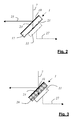
- Fig. 1 shows a device for light power measurement according to the prior art Technology.
- the device comprises a beam splitter 1, which is made of a substrate 3 with a partially reflective coating 5.
- the incident light beam 7 hits the coating 5 by reflection Split measuring light 9 onto the at a distance of about 3 cm arranged detector 11 hits.
- the division ratio is approx. 50: 1.
- the through the coating part of the light beam 7 experiences at the uncoated interface 13 of the substrate 3 a further unwanted cleavage.
- Another measuring light 15, the power of which is approximately 4% of the power of the part of the light beam 7 that has passed through the coating is on the interface 13 to the detector 11 is reflected.
- the coating split measuring light 9 interferes at the detector with that at the uncoated interface 13 of the substrate 3 split measurement light 15. Even the slightest variations in the optical path length between the Beam splitter 1 and the detector 11 and in the substrate 3, for example by Temperature changes, air pressure fluctuations or vibrations lead to a change in interference that results in a large variation in the measured light output.
- Fig. 2 shows an inventive device for determining the Light output of a light beam 7.
- the device comprises a beam splitter 1 with a substrate 17, which has a smooth surface with a partially permeable, metallic coating 19 and a roughened, diffuse has scattering surface 21.
- a detector 11 which is designed as a photodiode, cemented.
- the light beam 7 striking the beam splitter 1 is shown in transmitted measurement light 23 and a reflected partial beam 25 in the ratio 1:40 divided. Due to the roughened surface 21, the interference ability of the the detector 11 striking light largely destroyed.
- the device is on Due to the small design extremely insensitive to external interference.
- the Detector generates a measuring light 23 for the performance of the incident light proportional electrical signal that line 27 through it a Processing unit can be fed
- the device includes a beam splitter 1, which is a substrate made of frosted glass 29 and a partially reflective, dielectric Coating 31.
- the light beam 7 striking the coating is reflected to 97%.
- the measuring light 23 passing through the coating becomes Scattered in the milk glass substrate 29 and reaches the detector 11 largely destroyed interference ability.
- the detector generates a Power of the incident measuring light 23 proportional electrical signal, which can be fed via line 27 to a processing unit
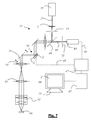
- Fig. 4 shows schematically an inventive microscope 33, which as confocal scanning microscope is executed.
- the one from a lighting system 35 coming illuminating light beam 37 is transmitted via a glass fiber 39 transports and hits after decoupling from the glass fiber 39 with the help of Optics 41 on a device 43 for determining the performance of the Illuminating light beam with a beam splitter 1
- a measuring beam divides the illuminating light beam and feeds it to the detector 11.
- the Beam splitter 1 contains a substrate made of frosted glass.
- the detector 11 generates an electrical signal proportional to the power of the measuring light line 45 is routed to processing unit 47.
- About one Beam splitter 49 passes the illuminating light beam 37 to the gimbal suspended scanning mirror 51, which the beam through the scanning optics 53, the Tube optics 55 and the objective 57 through or through the sample 59 leads.
- the illumination light beam 37 becomes 59 in the case of non-transparent samples passed over the sample surface.
- the illuminating light beam 37 can also pass through the sample 59 are performed. This means that from different Focal planes of the object successively through the illuminating light beam 37 be scanned.
- the subsequent composition then gives a three-dimensional image of the sample.
- a detector device 63 electrical, proportional to the power of the detection light Detection signals generated and via line 65 to the processing unit 47 passed on.
- the incoming, Analog signals are first digitized and then digitally offset and determines a corrected detection light power. This is connected to a PC 67 passed on.
- the corrected detection light output is based on a Position signal of the gimbaled mirror the position of the associated grid point and the data of all grid points an image of the sample 69, which is shown on a display 71 is shown.
- illumination pinhole 73 and the detection pinhole 75 are the Drawn schematically for completeness. Are omitted because of for better clarity, however, some optical elements for guidance and shaping the light rays. These are one that are active in this area Well known to those skilled in the art.
- FIG. 5 shows a further device according to the invention for determining the Light output of a light beam 7.
- a detector 11 is cemented to the substrate.
- the optical properties of the cement 83 are based on the refractive index of the Glass substrates and the refractive index of the entrance window of the detector 11 adjusted so that reflections are largely avoided. Too Preventing errors due to the occurrence of reflected light 85 is the Detector arranged so that the optical path of the reflected light leads past the detector 11.
- FIG. 6 schematically shows a further microscope 33 according to the invention is designed as a confocal scanning microscope.
- the microscope 33 shown largely corresponds to the microscope shown in FIG. 4.
- the device 43 to determine the power of the illuminating light beam is in this Execution between the illumination pinhole 73 and the beam splitter 49 arranged.
- FIG. 7 schematically shows a further microscope 33 according to the invention is designed as a confocal scanning microscope.
- the microscope 33 shown largely corresponds to the microscope shown in FIG. 4.
- the device 43 to determine the power of the illuminating light beam is in this Execution between the gimbaled scan mirror 51 and the Scanning optics 53 arranged.
- the microscope 33 has the additional advantage that even fluctuations in the performance of a polarized Illumination light beam 37 are detected because of different Reflectivities of the beam splitter 49 for different ones Polarization directions, on fluctuations in the polarization direction are due.
Landscapes
- Physics & Mathematics (AREA)
- General Physics & Mathematics (AREA)
- Optics & Photonics (AREA)
- Spectroscopy & Molecular Physics (AREA)
- Chemical & Material Sciences (AREA)
- Analytical Chemistry (AREA)
- Microscoopes, Condenser (AREA)
- Mechanical Optical Scanning Systems (AREA)
Abstract
Description
- Ermitteln einer Lichtleistung eines Beleuchtungslichtstrahls mit einer Vorrichtung, die einen Strahlteiler und einen dem Strahlteiler zugeordneten Detektor umfasst, wobei der Strahlteiler Messlicht aus dem Beleuchtungslichtstrahl abspaltet und dem Detektor zuführt und das Verhältnis der Lichtleistung des Beleuchtungslichtstrahls zu der am Detektor gemessenen Lichtleistung des Messlichts zeitlich konstant ist.
- Ermitteln einer Lichtleistung eines von einer Probe ausgehenden Detektionslichtstrahles und
- Ermitteln einer korrigierten Lichtleistung durch Verrechnen der Lichtleistung des Beleuchtungslichtstrahles und der Lichtleistung des Detektionslichtstrahles.
- Fig. 1
- eine bekannte Vorrichtung zur Lichtleistungsmessung,
- Fig. 2
- eine erfindungsgemäße Vorrichtung zur Ermittlung der Lichtleistung eines Lichtstrahles,
- Fig. 3
- eine weitere erfindungsgemäße Vorrichtung zur Ermittlung der Lichtleistung eines Lichtstrahles,
- Fig. 4
- ein erfindungsgemäßes Mikroskop,
- Fig. 5
- eine weitere erfindungsgemäße Vorrichtung zur Ermittlung der Lichtleistung eines Lichtstrahles,
- Fig. 6
- ein weiteres erfindungsgemäßes Mikroskop und
- Fig. 7
- ein weiteres erfindungsgemäßes Mikroskop
Claims (19)
- Vorrichtung zur Ermittlung der Lichtleistung eines Lichtstrahles (7) mit einem Strahlteiler (1) und einem dem Strahlteiler (1) zugeordnetem Detektor (11), dadurch gekennzeichnet, dass der Strahlteiler (1) Messlicht (23) aus dem Lichtstrahl abspaltet und dem Detektor (11) zuführt, dass das Verhältnis der Lichtleistung des Lichtstrahles (7) zu der am Detektor (11) gemessenen Lichtleistung des Messlichts (23) zeitlich konstant ist und dass der Strahlteiler (1) und der Detektor (11) zu einer Einheit zusammengefasst sind.
- Vorrichtung nach Anspruch 1, dadurch gekennzeichnet, dass der Detektor (11) unmittelbar hinter dem Strahlteiler (1) angeordnet ist.
- Vorrichtung nach einem der Ansprüche 1 bis 2, dadurch gekennzeichnet, dass der Strahlteiler (1) eine Beschichtung (19, 31) aufweist, die auf dem Substrat (17, 29) aufgebracht ist.
- Vorrichtung nach Anspruch 3, dadurch gekennzeichnet, dass die Beschichtung (19, 31) eine metallische Beschichtung ist.
- Vorrichtung nach Anspruch 1, dadurch gekennzeichnet, dass das Substrat (17, 29) zumindest eine streuende Fläche (21) aufweist oder dass das Substrat (17, 29) zumindest teilweise aus Milchglas besteht.
- Vorrichtung nach einem der Ansprüche 1 bis 5, dadurch gekennzeichnet, dass der Strahlteiler (1) transmittiertes Messlicht (79) und einen reflektierten Teilstrahl (25) erzeugt und ausschließlich das transmittierte Messlicht (79) auf den Detektor (11) trifft.
- Vorrichtung nach Anspruch 1, dadurch gekennzeichnet, dass das Verhältnis der Lichtleistungen des Lichtstrahles (7) zu der am Detektor (11) gemessenen Lichtleistung des Messlichtes (23) weitgehend unabhängig von der Wellenlänge des Lichtstrahles (7) ist.
- Mikroskop (33) mit einer Lichtquelle, die einen Beleuchtungslichtstrahl (37) zur Beleuchtung einer Probe (59) emittiert, mit mindestens einer Detektorvorrichtung (63) zur Detektion des von der Probe (59) ausgehenden Detektionslichtes (61) und einer Vorrichtung zur Ermittlung der Lichtleistung eines Beleuchtungslichtstrahls (37) mit einem Strahlteiler und einem dem Strahlteiler zugeordnetem Detektor, dadurch gekennzeichnet, dass der Strahlteiler Messlicht aus dem Beleuchtungslichtstrahl (37) abspaltet und dem Detektor zuführt, dass das Verhältnis der Lichtleistung des Beleuchtungslichtstrahls (37) zu der am Detektor gemessenen Lichtleistung des Messlichts zeitlich konstant ist, und dass der Strahlteiler (1) und der Detektor (11) zu einer Einheit zusammengefasst sind.
- Mikroskop (33) nach Anspruch 8, dadurch gekennzeichnet, dass die Einheit ein Gehäuse aufweist.
- Mikroskop (33) nach einem der Ansprüche 8 bis 9, dadurch gekennzeichnet, dass der Detektor (11) unmittelbar hinter dem Strahlteiler (1) angeordnet ist.
- Mikroskop (33) nach einem der Ansprüche 8 bis 10, dadurch gekennzeichnet, dass der Strahlteiler (1) eine Beschichtung (19, 31) aufweist, die auf dem Substrat (17, 29) aufgebracht ist.
- Mikroskop (33) nach Anspruch 11, dadurch gekennzeichnet, dass das Substrat (17, 29) zumindest eine streuende Fläche (21) aufweist oder dass das Substrat (17, 29) zumindest teilweise aus Milchglas besteht.
- Mikroskop (33) nach Anspruch 8, dadurch gekennzeichnet, dass das Verhältnis der Lichtleistungen des Beleuchtungslichtstrahls (37) zu der am Detektor (11) gemessenen Lichtleistung des Messlichtes (23) weitgehend unabhängig von der Wellenlänge des Beleuchtungslichtstrahls (37) ist.
- Mikroskop (33) nach einem der Ansprüche 8 bis 13, dadurch gekennzeichnet, dass das Mikroskop (33) ein Scanmikroskop oder ein konfokales Scanmikroskop ist.
- Verfahren zur Mikroskopie gekennzeichnet durch folgende Schritte:Ermitteln einer Lichtleistung eines Beleuchtungslichtstrahles (37) mit einer Vorrichtung, die einen Strahlteiler (1) und einem dem Strahlteiler (1) zugeordnetem Detektor (11) umfasst, wobei der Strahlteiler (1) Messlicht (23) aus dem Beleuchtungslichtstrahl (37) abspaltet und dem Detektor (11) zuführt und das Verhältnis der Lichtleistung des Beleuchtungslichtstrahles (37) zu der am Detektor (11) gemessenen Lichtleistung des Messlichts (23) zeitlich konstant ist.Ermitteln einer Lichtleistung eines von einer Probe (59) ausgehenden Detektionslichtstrahles undErmitteln einer korrigierten Lichtleistung durch Verrechnen der Lichtleistung des Beleuchtungslichtstrahles (37) und der Lichtleistung des Detektionslichtstrahles.
- Verfahren nach Anspruch 15, dadurch gekennzeichnet, dass das Ermitteln der Lichtleistung des Beleuchtungslichtstrahles (37) und des Detektionslichtstrahles simultan erfolgt.
- Verfahren nach Anspruch 15, dadurch gekennzeichnet, dass das Ermitteln der Lichtleistung des Beleuchtungslichtstrahls (37) einen Offsetabgleich umfasst.
- Verfahren nach Anspruch 15, dadurch gekennzeichnet, dass das Ermitteln der Lichtleistung des Detektionslichtstrahles einen Offsetabgleich umfasst.
- Verfahren nach einem der Ansprüche 15 bis 18, dadurch gekennzeichnet, dass das Ermitteln einen Skalierungsschritt umfasst.
Applications Claiming Priority (2)
| Application Number | Priority Date | Filing Date | Title |
|---|---|---|---|
| DE10125469A DE10125469B4 (de) | 2001-05-25 | 2001-05-25 | Vorrichtung zur Ermittlung einer Lichtleistung, Mikroskop und Verfahren zur Mikroskopie |
| DE10125469 | 2001-05-25 |
Publications (3)
| Publication Number | Publication Date |
|---|---|
| EP1260848A2 true EP1260848A2 (de) | 2002-11-27 |
| EP1260848A3 EP1260848A3 (de) | 2002-12-18 |
| EP1260848B1 EP1260848B1 (de) | 2005-07-20 |
Family
ID=7686078
Family Applications (1)
| Application Number | Title | Priority Date | Filing Date |
|---|---|---|---|
| EP02100561A Expired - Lifetime EP1260848B1 (de) | 2001-05-25 | 2002-05-24 | Vorrichtung zur Ermittlung einer Lichtleistung, Mikroskop und Verfahren zur Mikroskopie |
Country Status (4)
| Country | Link |
|---|---|
| US (1) | US6806950B2 (de) |
| EP (1) | EP1260848B1 (de) |
| JP (1) | JP2003075764A (de) |
| DE (2) | DE10125469B4 (de) |
Families Citing this family (8)
| Publication number | Priority date | Publication date | Assignee | Title |
|---|---|---|---|---|
| DE10324478B3 (de) * | 2003-05-30 | 2004-12-09 | Leica Microsystems Heidelberg Gmbh | Vorrichtung zum Ermitteln der Lichtleistung eines Lichtstrahles und Scanmikroskop |
| US6970295B1 (en) * | 2004-06-16 | 2005-11-29 | Leadlight Technology, Inc. | Optical beam expander with a function of laser power detection |
| US20080079945A1 (en) * | 2006-10-02 | 2008-04-03 | Flowers John P | Apparatus and Method to Quantify Laser Head Reference Signal Reliability |
| DE102008055655B4 (de) * | 2008-10-29 | 2021-04-08 | Carl Zeiss Microscopy Gmbh | Verfahren zur Einstellung eines Dunkelsignals einer Laserquelle in einem Laser- Scanning-Mikroskop |
| DE102016122528A1 (de) | 2016-11-22 | 2018-05-24 | Carl Zeiss Microscopy Gmbh | Verfahren zum Steuern oder Regeln einer Mikroskopbeleuchtung |
| DE102016122529A1 (de) | 2016-11-22 | 2018-05-24 | Carl Zeiss Microscopy Gmbh | Mikroskop zur Abbildung eines Objekts |
| EP4051997A4 (de) * | 2019-10-31 | 2023-11-15 | Wi-Charge Ltd. | Optischer leistungsmesser zum sicheren betrieb von optischen drahtlosen leistungssystemen |
| US11822033B2 (en) | 2019-12-16 | 2023-11-21 | Halliburton Energy Services, Inc. | Radiometric modeling for optical identification of sample materials |
Family Cites Families (20)
| Publication number | Priority date | Publication date | Assignee | Title |
|---|---|---|---|---|
| JPS55137508A (en) * | 1979-04-13 | 1980-10-27 | Matsushita Electric Ind Co Ltd | Photocoupler |
| ES252713Y (es) * | 1979-08-27 | 1981-11-16 | Un divisor optico de haz luminoso mejorado | |
| US4375680A (en) * | 1981-01-16 | 1983-03-01 | Mcdonnell Douglas Corporation | Optical acoustic sensor |
| NL8104588A (nl) | 1981-10-08 | 1983-05-02 | Philips Nv | Bundelscheidingsprisma, werkwijze voor het vervaardigen van dit prisma en van dit prisma voorziene optische lees- en/of schrijfeenheid. |
| NL8303932A (nl) | 1982-11-17 | 1984-06-18 | Pioneer Electronic Corp | Opneeminrichting voor optische plaat. |
| DE3484723D1 (de) | 1983-09-05 | 1991-07-25 | Mitsubishi Electric Corp | Automatisches fokussierungsverfahren. |
| JPS60187941A (ja) | 1984-03-08 | 1985-09-25 | Seiko Instr & Electronics Ltd | 光情報検出装置 |
| JPS61289544A (ja) | 1985-06-14 | 1986-12-19 | Canon Inc | 光ヘツド装置 |
| JPS621141A (ja) | 1985-06-27 | 1987-01-07 | Matsushita Electric Ind Co Ltd | 光学ヘツド |
| DE3887762T2 (de) | 1987-03-17 | 1994-09-08 | Matsushita Electric Ind Co Ltd | Optischer Kopf. |
| US5475491A (en) * | 1989-02-10 | 1995-12-12 | Canon Kabushiki Kaisha | Exposure apparatus |
| JPH04301236A (ja) * | 1991-03-28 | 1992-10-23 | Canon Inc | 光学装置 |
| US5459611A (en) * | 1993-08-18 | 1995-10-17 | Hewlett-Packard Company | Beam splitter/combiner with path length compensator and method for making the same |
| US6309601B1 (en) * | 1993-11-01 | 2001-10-30 | Nanogen, Inc. | Scanning optical detection system |
| DE59609547D1 (de) * | 1995-05-17 | 2002-09-12 | Leica Mikroskopie Systeme Ag H | Mikroskop |
| DE59702158D1 (de) * | 1996-09-30 | 2000-09-14 | Siemens Ag | Verfahren zum herstellen eines strahlteilerformkörpers und verwendung des strahlteilerformkörpers in einem optoelektronischen modul |
| DE19758744C2 (de) * | 1997-01-27 | 2003-08-07 | Zeiss Carl Jena Gmbh | Laser-Scanning-Mikroskop |
| US6507419B1 (en) * | 1999-03-23 | 2003-01-14 | Digilens, Inc. | Illumination system using optical feedback |
| US6496261B1 (en) * | 1999-09-24 | 2002-12-17 | Schlumberger Technologies, Inc. | Double-pulsed optical interferometer for waveform probing of integrated circuits |
| DE60121439T2 (de) * | 2001-08-30 | 2007-01-11 | Instrumentarium Corp. | Geometrischer Strahlteiler und Sensor mit einem Detektor aus mehreren Elementen |
-
2001
- 2001-05-25 DE DE10125469A patent/DE10125469B4/de not_active Expired - Lifetime
-
2002
- 2002-05-24 DE DE50203658T patent/DE50203658D1/de not_active Expired - Lifetime
- 2002-05-24 US US10/154,938 patent/US6806950B2/en not_active Expired - Lifetime
- 2002-05-24 EP EP02100561A patent/EP1260848B1/de not_active Expired - Lifetime
- 2002-05-27 JP JP2002152540A patent/JP2003075764A/ja active Pending
Also Published As
| Publication number | Publication date |
|---|---|
| DE10125469A1 (de) | 2002-12-12 |
| EP1260848A3 (de) | 2002-12-18 |
| US6806950B2 (en) | 2004-10-19 |
| DE10125469B4 (de) | 2008-01-10 |
| JP2003075764A (ja) | 2003-03-12 |
| US20020191177A1 (en) | 2002-12-19 |
| EP1260848B1 (de) | 2005-07-20 |
| DE50203658D1 (de) | 2005-08-25 |
Similar Documents
| Publication | Publication Date | Title |
|---|---|---|
| US8587772B2 (en) | Chromatic point sensor configuration including real time spectrum compensation | |
| DE102008029459B4 (de) | Verfahren und Vorrichtung zur berührungslosen Abstandsmessung | |
| DE2354141C2 (de) | Optisches Meßverfahren zum Untersuchen von Oberflächen und Einrichtung zur Durchführung des Verfahrens | |
| DE3203613A1 (de) | Entfernungsmessvorrichtung | |
| CH654914A5 (de) | Optoelektronisches messverfahren und einrichtung zum bestimmen der oberflaechenguete streuend reflektierender oder transparenter oberflaechen. | |
| WO1993011403A1 (de) | Optischer abstandssensor | |
| DE4211875A1 (de) | Optischer Abstandssensor | |
| CA2334225C (en) | Method and device for opto-electrical acquisition of shapes by axial illumination | |
| DE3784231T2 (de) | Verfahren und vorrichtung zur beruehrungslosen automatischen fokussierung. | |
| EP1260848B1 (de) | Vorrichtung zur Ermittlung einer Lichtleistung, Mikroskop und Verfahren zur Mikroskopie | |
| DE10125885B4 (de) | Sensorvorrichtung zur schnellen optischen Abstandsmessung nach dem konfokalen optischen Abbildungsprinzip | |
| DE10107210C1 (de) | Mikroskop | |
| DE19637131C2 (de) | Einrichtung zum Beurteilen des Reflexionsverhaltens eines Objektes, insbesondere einer Flüssigkristallanzeige | |
| EP0585893A1 (de) | Verfahren und Vorrichtung zur hochgenauen Abstandsmessung von Oberflächen | |
| DE10021379A1 (de) | Optische Messanordnung insbesondere zur Schichtdickenmessung | |
| DE10324478B3 (de) | Vorrichtung zum Ermitteln der Lichtleistung eines Lichtstrahles und Scanmikroskop | |
| DE10142945A1 (de) | Vorrichtung zur Ermittlung einer Lichtleistung und Mikroskop | |
| EP1353210B1 (de) | Mikroskop mit einer Vorrichtung zur Ermittlung der Lichtleistung eines Beleuchtungslichtstrahls | |
| DE102019102873B4 (de) | Sensorsystem und Verfahren zur Bestimmung von geometrischen Eigenschaften eines Messobjekts sowie Koordinatenmessgerät | |
| DE19828454B4 (de) | Vorrichtung und Verfahren zur Messung der Temperatur einer Zielfläche | |
| DE102018212685B4 (de) | Optische Partikelsensorvorrichtung und entsprechendes Partikelmessverfahren | |
| JPS63295945A (ja) | 光沢度測定装置 | |
| DE19707225A1 (de) | Lichtabtastvorrichtung | |
| CN119948310A (zh) | 包括摄像机的彩色共焦测量设备 | |
| EP0318566B1 (de) | Optischer abtastkopf |
Legal Events
| Date | Code | Title | Description |
|---|---|---|---|
| PUAI | Public reference made under article 153(3) epc to a published international application that has entered the european phase |
Free format text: ORIGINAL CODE: 0009012 |
|
| PUAL | Search report despatched |
Free format text: ORIGINAL CODE: 0009013 |
|
| AK | Designated contracting states |
Kind code of ref document: A2 Designated state(s): AT BE CH CY DE DK ES FI FR GB GR IE IT LI LU MC NL PT SE TR |
|
| AX | Request for extension of the european patent |
Free format text: AL;LT;LV;MK;RO;SI |
|
| AK | Designated contracting states |
Kind code of ref document: A3 Designated state(s): AT BE CH CY DE DK ES FI FR GB GR IE IT LI LU MC NL PT SE TR |
|
| AX | Request for extension of the european patent |
Free format text: AL;LT;LV;MK;RO;SI |
|
| 17P | Request for examination filed |
Effective date: 20030522 |
|
| AKX | Designation fees paid |
Designated state(s): DE FR GB |
|
| 17Q | First examination report despatched |
Effective date: 20030811 |
|
| GRAP | Despatch of communication of intention to grant a patent |
Free format text: ORIGINAL CODE: EPIDOSNIGR1 |
|
| GRAS | Grant fee paid |
Free format text: ORIGINAL CODE: EPIDOSNIGR3 |
|
| GRAA | (expected) grant |
Free format text: ORIGINAL CODE: 0009210 |
|
| AK | Designated contracting states |
Kind code of ref document: B1 Designated state(s): DE FR GB |
|
| REG | Reference to a national code |
Ref country code: GB Ref legal event code: FG4D Free format text: NOT ENGLISH |
|
| REF | Corresponds to: |
Ref document number: 50203658 Country of ref document: DE Date of ref document: 20050825 Kind code of ref document: P |
|
| GBT | Gb: translation of ep patent filed (gb section 77(6)(a)/1977) |
Effective date: 20051003 |
|
| ET | Fr: translation filed | ||
| RAP2 | Party data changed (patent owner data changed or rights of a patent transferred) |
Owner name: LEICA MICROSYSTEMS CMS GMBH |
|
| PLBE | No opposition filed within time limit |
Free format text: ORIGINAL CODE: 0009261 |
|
| STAA | Information on the status of an ep patent application or granted ep patent |
Free format text: STATUS: NO OPPOSITION FILED WITHIN TIME LIMIT |
|
| 26N | No opposition filed |
Effective date: 20060421 |
|
| REG | Reference to a national code |
Ref country code: FR Ref legal event code: TP |
|
| REG | Reference to a national code |
Ref country code: GB Ref legal event code: 732E |
|
| REG | Reference to a national code |
Ref country code: FR Ref legal event code: PLFP Year of fee payment: 14 |
|
| REG | Reference to a national code |
Ref country code: FR Ref legal event code: PLFP Year of fee payment: 15 |
|
| REG | Reference to a national code |
Ref country code: FR Ref legal event code: PLFP Year of fee payment: 16 |
|
| REG | Reference to a national code |
Ref country code: FR Ref legal event code: PLFP Year of fee payment: 17 |
|
| PGFP | Annual fee paid to national office [announced via postgrant information from national office to epo] |
Ref country code: FR Payment date: 20210526 Year of fee payment: 20 |
|
| PGFP | Annual fee paid to national office [announced via postgrant information from national office to epo] |
Ref country code: GB Payment date: 20210526 Year of fee payment: 20 |
|
| PGFP | Annual fee paid to national office [announced via postgrant information from national office to epo] |
Ref country code: DE Payment date: 20210729 Year of fee payment: 20 |
|
| REG | Reference to a national code |
Ref country code: DE Ref legal event code: R071 Ref document number: 50203658 Country of ref document: DE |
|
| REG | Reference to a national code |
Ref country code: GB Ref legal event code: PE20 Expiry date: 20220523 |
|
| PG25 | Lapsed in a contracting state [announced via postgrant information from national office to epo] |
Ref country code: GB Free format text: LAPSE BECAUSE OF EXPIRATION OF PROTECTION Effective date: 20220523 |