EP1260936A2 - Erfassungsvorrichtung zur Erkennung von Oberflächenmustern - Google Patents
Erfassungsvorrichtung zur Erkennung von Oberflächenmustern Download PDFInfo
- Publication number
- EP1260936A2 EP1260936A2 EP02090171A EP02090171A EP1260936A2 EP 1260936 A2 EP1260936 A2 EP 1260936A2 EP 02090171 A EP02090171 A EP 02090171A EP 02090171 A EP02090171 A EP 02090171A EP 1260936 A2 EP1260936 A2 EP 1260936A2
- Authority
- EP
- European Patent Office
- Prior art keywords
- circuit
- transistor
- sensor
- signal
- word lines
- Prior art date
- Legal status (The legal status is an assumption and is not a legal conclusion. Google has not performed a legal analysis and makes no representation as to the accuracy of the status listed.)
- Granted
Links
Images


Classifications
-
- G—PHYSICS
- G06—COMPUTING OR CALCULATING; COUNTING
- G06V—IMAGE OR VIDEO RECOGNITION OR UNDERSTANDING
- G06V40/00—Recognition of biometric, human-related or animal-related patterns in image or video data
- G06V40/10—Human or animal bodies, e.g. vehicle occupants or pedestrians; Body parts, e.g. hands
- G06V40/12—Fingerprints or palmprints
- G06V40/13—Sensors therefor
- G06V40/1306—Sensors therefor non-optical, e.g. ultrasonic or capacitive sensing
Definitions
- the present invention relates to a surface shape recognition sensor device and, more particularly, to a surface shape recognition sensor device which senses a fine three-dimensional pattern such as a human fingerprint or animal noseprint.
- a sensor electrode is formed in each of cells (to be referred to as sensor cells hereinafter) that are two-dimensionally arrayed on an LSI chip.
- An electrostatic capacitance formed between the sensor electrode and the skin surface of a finger that comes into contact with the sensor electrode via an insulating film is detected, thereby sensing the three-dimensional pattern of the skin surface. Since the capacitance changes depending on the three-dimensional pattern of the skin surface, the three-dimensional pattern of the skin surface can be sensed by detecting the capacitance difference.
- a surface shape recognition sensor device having a means for individually adjusting the detection sensitivities of a plurality of sensor circuits is supposed.
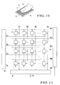
- Fig. 10 shows a use state of a surface shape recognition sensor device having a detection sensitivity adjusting function.
- This surface shape recognition sensor device is constructed by a number of sensor cells adjacent to each other.
- the surface shape recognition sensor device is formed from a number 11 two-dimensionally arranged (in an array or grid shape) sensor cells 11.
- An object to be detected such as a finger 13 is brought into contact with a sensor surface 12 of a surface shape recognition sensor device 10.
- a surface (three-dimensional shape of a fingerprint) 14 to be detected is individually detected by each sensor cell 11, and two-dimensional data representing the surface shape of the object is output.
- Fig. 11 shows the entire arrangement of the conventional surface shape recognition sensor device.
- the sensor cells 11 are arranged in a two-dimensional matrix with p rows ⁇ q columns.
- the sensor cells 11 are connected to word lines WL1 to WLp for selectively controlling the sensor cells 11 and data lines DL1 to DLq for propagating the outputs from the sensor cells 11 so as to form a grid shape.
- a decoder 20 and A/D conversion circuit 30 are arranged in the periphery of the sensor cells 11.
- the decoder 20 controls the word lines in accordance with a received address signal ADR.
- the A/D conversion circuit 30 converts analog signals received from the data lines into a digital signal and outputs it.
- a plurality of sensor cells 11 is sequentially selected by the decoder 20, and the analog outputs from the sensor cells 11 are converted into digital outputs by the A/D conversion circuit 30.
- the sensor cells 11 share the A/D conversion circuit 30.
- the surface shape recognition sensor device 10 has a function of adjusting (to be referred to as calibration hereinafter) the sensitivity of each sensor cell to uniform a variation in characteristic, i.e., detection sensitivity between the sensor cells 11 due to the manufacturing process.
- calibration mode signal lines CL1 to CLp are connected to the of sensor cells 11, like the word lines WL1 to WLp.
- a calibration control circuit 40 sequentially selects a plurality of sensor cells and sequentially calibrates the selected sensor cells.
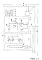
- Fig. 12 shows a conventional sensor cell.
- the sensor cell 11 is formed from a detection element 1, a sensor circuit 2, a calibration circuit 3, and a selection circuit 4.
- the detection element 1 converts a surface shape into an electric amount.
- the sensor circuit 2 measures the electric amount of the detection element, which changes depending on the surface shape, causes an internal voltage-time conversion circuit (to be referred to as a VT conversion circuit hereinafter) 21 to convert the electric amount into a time signal having a pulse width corresponding to the electric amount, and outputs the time signal as an output signal 2A.
- a VT conversion circuit an internal voltage-time conversion circuit
- the calibration circuit 3 individually executes adjustment (sensitivity adjustment) of the detection sensitivity of the sensor circuit 2 in each sensor cell 11.
- the selection circuit 4 sets the sensor cell 11 in an operative state on the basis of the active state of the word line WL or the calibration mode signal from the calibration mode signal line CL.
- a reference sample without any three-dimensional pattern is detected by the sensor, or detection is performed without placing anything on the sensor surface, thereby causing the respective sensor cells 11 to detect the same measurement value.
- the output signal 2A from each sensor cell 11 is input to the calibration circuit 3 of that sensor cell.
- the calibration circuit 3 is formed from a load circuit 31, a counter circuit (n-bit) 32, and a time signal comparison circuit 33.
- the time signal comparison circuit 33 compares the output signal 2A with a reference pulse signal 3A having a pulse width corresponding to a desired detection sensitivity. A comparison result having a pulse width corresponding to the difference between them is input to the counter circuit (n-bit) 32 as a counter input signal 3B.
- the counter circuit 32 executes new counter operation on the basis of the counter input signal 3B.
- the count data of the counter circuit 32 is sequentially updated.
- Connection of the sensor circuit 2 to n load elements Z 1 to Z n arranged in the load circuit 31 is controlled on the basis of the count data so that the detection sensitivity of the sensor circuit 2 is adjusted.
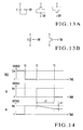
- Figs. 13A and 13B show implementation examples of load elements that can be controlled to active and inactive states.
- Fig. 13A shows capacitive load elements.
- Fig. 13B shows resistive load elements.
- an electrostatic capacitance formed between the finger surface 14 and a sensor electrode 1B is used as the electric amount
- one of the load elements shown in Fig. 13A is used.
- a contact resistance formed between the finger surface 14 and the sensor electrode 1B is used as the electric amount
- one of the load elements shown in Fig. 13B is used.
- This operation is repeated a number of times corresponding to the number of adjustment stages, e.g., 2 n -1 times except a state wherein all load elements Z are unselected, thereby adjusting the detection sensitivity of each sensor circuit 2 and uniforming the performance of the sensor cells.
- the detection element 1 is implemented by the sensor electrode 1B formed on an insulating layer 16 and covered with a passivation film 15. As the electric amount, an electrostatic capacitance C f formed between the finger surface 14 and the sensor electrode 1B is used.
- the sensor circuit 2 is formed from a Pch MOSFET Q 1 , an Nch MOSFET Q 2 , an constant current source I, and the VT conversion circuit 21.
- Reference symbol C p0 denotes a parasitic capacitance.
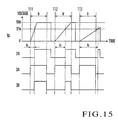
- Fig. 14 shows the detection operation of a sensor cell.
- a sensor circuit control signal PRE is controlled to a power supply voltage V DD to turn off the Pch MOSFET Q 1 .
- a sensor circuit control signal RE is controlled to 0 V to turn off the Nch MOSFET Q 2 .
- a node N 1 is set at 0 V.
- the signal PRE is controlled to 0 V to turn on the Pch MOSFET Q 1 .
- the potential of the node N 1 rises up to V DD .
- the signals PRE and RE are controlled to V DD to turn off the Pch MOSFET Q 1 and turn on the Nch MOSFET Q 2 . With this operation, charges accumulated in the electrostatic capacitance C f are removed.
- the potential of the node N 1 gradually drops at a rate depending on the electrostatic capacitance C f .
- the signal RE is controlled to 0 V to turn off the Nch MOSFET Q 2 .
- a potential V DD - ⁇ V corresponding to the electrostatic capacitance C f is maintained. This potential is output to the VT conversion circuit 21.
- the VT conversion circuit 21 has a constant current source I VT , a capacitance C L , and a threshold value circuit 22.
- the constant current source I VT operates in accordance with the potential of the node N 1 to charge the capacitance C L .
- the threshold value circuit 22 inverts its output, i.e., the output signal 2A.
- the output signal 2A is inverted after the elapse of a time corresponding to the potential of the node N 1 from the start of charge accumulation in the empty capacitance C L . In sensing operation of detecting the surface shape of an object to be detected, this time length is measured, thereby detecting the three-dimensional pattern of the skin surface.
- the time signal comparison circuit 33 operates on the basis of a calibration signal CAL from the calibration control circuit 40, and calibration by the calibration circuit 3 is executed.
- count data in the counter circuit 32 is set to the initial set value in advance to set all load elements in an inactive state.
- the output signal 2A from the VT conversion circuit 21 is set to the initial set value at the start of individual detection operation.
- the reference pulse signal 3A having a pulse width corresponding to a desired detection sensitivity is supplied to the sensor cell 11. In synchronism with this, the sensor cells 11 sequentially execute detection operation.
- the output signal 2A is obtained from the sensor circuit 2.
- the time signal comparison circuit 33 compares the output signal 2A with the reference pulse signal 3A. For example, the output signal 2A and reference pulse signal 3A are ANDed to generate the counter input signal 3B.
- delay time ts from the leading edge of the reference pulse signal 3A to the leading edge of the output signal 2A changes in accordance with the load in the load circuit 31.
- the counter input signal 3B is input to the counter circuit 32 for every detection operation. Hence, the counter circuit 32 increments the count data, and the load of the load circuit 31 sequentially increases.
- the detection sensitivity of the sensor circuit 2 equals the desired sensitivity.
- the counter input signal 3B is not output anymore, and the selection state of the load elements at that time is held by the counter circuit 32.
- Z k Z ⁇ 2 k-1 (k is a natural number) is set. Every time the count data is incremented, the value of the load circuit 31 is increased by Z.
- the detection sensitivity can be adjusted in Z increments.
- Such calibration operation is individually executed for the respective sensor cells 11 to adjust them to an appropriate detection sensitivity. Even when the characteristic, i.e., detection sensitivity of the sensor circuit 2 changes between the sensor cells due to the process variation, the sensor cells can have uniform detection performance.
- the present invention has been made to solve this problem, and has as its object to provide a surface shape recognition sensor device capable of calibrating the detection sensitivity of each sensor cell with a smaller circuit arrangement.
- the surface shape recognition sensor device used in the present invention performs, as operations of the surface shape recognition sensor device, a detection operation of recognizing a surface shape and a calibration operation of adjusting a sensor device.
- a detection operation of recognizing a surface shape In the surface shape detection operation, no calibration operation is executed.
- the calibration operation no surface shape detection operation is executed. That is, the calibration operation is executed between the surface shape detection operations or at an appropriate time. The two operations are not executed simultaneously.
- a surface shape recognition sensor device comprising a number of two-dimensionally arranged sensor cells, a decoder which selects a sensor cell, an output circuit which sends a sensor output from the selected sensor cell, a control circuit which sends an address signal to the decoder to select the sensor cell, and a calibration mode signal line which is commonly connected to the sensor cells and simultaneously supplies a calibration mode signal from the control circuit to the sensor cells to designate calibration, wherein each of the sensor cells comprises a detection element which detects an electric amount that changes according to the surface shape of an object, a sensor circuit which performs sensing operation of measuring the electric amount detected by the detection element, converting the electric amount into a corresponding output signal, and outputting the output signal, and a calibration circuit adjusting the detection sensitivity of the sensor circuit on the basis of the sensor output obtained by the sensing operation of the sensor circuit, and when the calibration mode signal is supplied from the control circuit to the sensor cells through the calibration mode signal line, on the basis of a
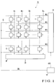
- sensor cells 11 are arranged in a two-dimensional matrix with p rows ⁇ q columns.
- the sensor cells 11 are connected to word lines WL1 to WLp for selectively controlling the sensor cells and data lines DL1 to DLq for propagating the outputs from the sensor cells 11 so as to form a grid shape.
- a decoder 20 and A/D conversion circuit 30 are arranged in the periphery of the sensor cells 11.
- the decoder 20 controls the word lines WL1 to WLp in accordance with an address signal ADR supplied from a control circuit 50.
- the A/D conversion circuit 30 converts analog signals received from the data lines DL1 to DLq into a digital output signal 3A and outputs it.
- the sensor cells 11 are commonly connected to a calibration mode signal line CL. In the calibration mode, the same calibration mode signal CAL is simultaneously supplied to the sensor cells 11 through the calibration mode signal line CL.
- the calibration mode signal CAL is sent from the control circuit 50.
- a normal surface shape detection operation mode or calibration operation mode is designated to the sensor cells 11 by the calibration mode signal CAL.
- the sensor cells 11 that should execute calibration can be selected by the decoder 20 used in the normal surface shape detection operation mode.
- the address signal ADR (ADB or ADW to be described later) and calibration mode signal CAL are supplied from the control circuit 50.
- the signals may be supplied from a host device such as a CPU that externally controls the surface shape recognition sensor device or may be independently generated in the surface shape recognition sensor device and supplied.
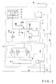
- each sensor cell 11 has almost the same arrangement as that of the above-described conventional sensor cell (Fig. 12).
- ame reference numerals as in Fig. 12 denote same or similar parts in Fig. 2.
- the calibration mode signal CAL is input to the selection circuit 4 to control the operation of the sensor cell itself, resulting in redundant arrangement.
- the word line WL is input to a selection circuit 4.
- the calibration mode signal CAL is input only to a time signal comparison circuit 33.
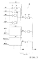
- Fig. 3 shows a detailed example of the decoder 20.
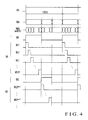
- Fig. 4 shows the operation of the decoder shown in Fig. 3.
- one block is formed every 2 m word lines WL (m is an integer: m ⁇ 2).
- Blocks 101, 102, 103,... are managed.
- a gate 110 which decodes an address value corresponding to a given word line WL, in the address signal ADW (m bits) for word line selection, and outputs a word line selection signal for activating the word line, and a buffer 111 which activates the word line WL in accordance with the word line selection signal from the gate 110 are arranged for each word line WL.
- a gate 120 (block selection circuit) which decodes an address value corresponding to a given block, in the address signal bit ADB for block selection, and a buffer 121 which supplies the output from the gate 120 to the gate 110 of the block as a block selection signal SB (SB1, SB2, SB3,...) are arranged in correspondence with each block.
- the block selection signal SB is output to one of the blocks in accordance with the address value of the address signal ADB.
- one of the word lines WL is activated by the output from one of the gates 110 that have received the block signal, which corresponds to the address value of the address signal ADW.
- address signals ADB and ADW complementary signals (for m bits, i.e., 2m signals) that indicate positive and negative logic levels for each address bit are used.
- address bits of positive or negative logic which change to high level in correspondence with the addresses of the word lines WL, are selectively input to the gates 110.
- the AND of the address bits is output as a word line selection signal.
- Address bits which change to high level in correspondence with the addresses of the blocks are selectively input to the gates 120.
- the AND of the address bits is output as a block selection signal.
- the calibration mode signal CAL (high level in Fig. 4) is supplied to all the sensor cells 11.
- the address signals ADB and ADW are sequentially changed to sequentially select the word lines.
- the block selection signal SB1 of the block 101 changes to high level to sequentially activate the word lines WL1 to WL2 n one by one.
- the block selection signal SB2 of the e block 101 is validated to sequentially activate the word lines WL2 m +1 to WL2 m+1 one by one.
- the above cycle is repeated a number of times corresponding to the number of adjustment stages of calibration.
- the calibration operation is executed for each sensor cell 11 a number of times equal to the number of adjustment stages.
- each sensor cell 11 The calibration operation in each sensor cell 11 is the same as that in Figs. 14 and 15 described above, and description thereof may be omitted.
- the calibration mode signal line CL to which the sensor cells 11 are commonly connected is arranged.
- a calibration mode signal (high level in Fig. 4) for designating calibration is supplied to the sensor cells through the calibration mode signal line.
- the calibration mode signal CAL is being supplied from the calibration mode signal line CL, and the sensor cell is selected by the decoder 20, calibration operation of adjusting the detection sensitivity of the sensor circuit 2 is executed using the calibration circuit 3. Since calibration can be done using the decoder that is used for normal sensing without adding any calibration control circuit, any increase in circuit scale can be suppressed.
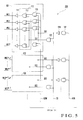
- Fig. 5 shows the second embodiment of the decoder 20A.
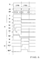
- Fig. 6 shows the operation of the decoder 20A.
- the word lines WL are selected one by one as in the normal surface shape detection operation.
- a plurality of word lines are selected simultaneously for each block.
- the decoder 20A is different from the decoder 20 in that a gate 122 that outputs the AND between a block selection signal SB and a multiplex selection control signal SS as a block multiplex selection control signal SSx (SS1, SS2, SS3,...) is arranged for each block, and a block multiplex selection control circuit 113 formed from gates 112 each arranged between a gate 110 and a buffer 111 of each word line WL is arranged in each block. Each gate 112 receives the output from the gate 110 of a corresponding word line WL and the block multiplex selection control signal SSx of the block. The exclusive-OR (EOR) of these inputs is output to the buffer 111.
- the multiplex selection control signal SS is sent from a control circuit 50 in the calibration mode.
- the multiplex selection control signal SS in the normal surface shape detection operation, is set at low level. For this reason, the block multiplex selection control signal SSx from the gate 122 of each block changes to low level, and each gate 112 in the block multiplex selection control circuit 113 operates as a buffer. With this operation, only one word line WL corresponding to address signals ADB and ADW is activated.
- the multiplex selection control signal SS and address signals ADB and ADW are sent from the control circuit 50.
- the signals may be supplied from a host device such as a CPU that externally controls the surface shape recognition sensor device or may be independently generated in the surface shape recognition sensor device and supplied.
- the block multiplex selection control signal SSx changes to high level only in a block selected by the address signal ADB.
- a calibration mode signal CAL (high level in Fig. 6) is supplied to all the sensor cells 11.
- a block selection signal SB1 of a block 101 changes to high level to sequentially select word lines WL1 to WL2 n , as shown in Fig. 6.
- n is the number of load elements Z in the calibration circuit 3.
- the block multiplex selection control signal SS1 is input from the gate 122 to the gates 112 in the block 101.
- Each gate 112 operates as an inverter. For this reason, in the word lines WL1 to WL2 n of the block 101, all word lines except one word line WL corresponding to the address value of the address signal ADW are activated.
- 2 n -1 word lines are multiplexed and selected by one address value of the address signal ADW.
- the word lines WL in the block are activated 2 n -1 times only by making one addressing cycle of the address values of the address signal ADW, i.e., in 2 n cycles.
- the selection operation is executed for each block, thereby performing calibration operation for each sensor cell 11 a number of times corresponding to the number of adjustment stages.
- the block multiplex selection control circuit 113 simultaneously selects, from the word lines WL belonging to the block, all word lines except a word line corresponding to the address signal ADW on the basis of the AND between the block selection signal SB of the block and the multiplex selection control signal SS supplied in the calibration mode.
- the invention is not limited to this.
- the block multiplex selection control circuit 113 may activate all word lines WL of the block selected by the address signal ADB.
- the time required for calibration can be considerably shortened, as in the above-described case. At this time, when the word lines are divided such that each block has word lines equal in number to the number of adjustment stages, i.e., the number of times of calibration operation, efficient calibration is possible.
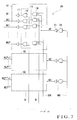
- Fig. 7 shows the third embodiment of the decoder 20B.
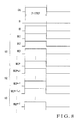
- Fig. 8 shows the operation of the decoder 20B shown in Fig. 7.
- a plurality of word lines WL are multiplexed and selected for each block in the calibration mode.
- all word lines are simultaneously selected instead of selecting them for each block.
- each block of the decoder 20B of this embodiment has a batch multiplex selection circuit 115 formed from gates 114 each arranged between a gate 110 and a buffer 111 of each word line WL.
- Each gate 114 receives the output from the gate 110 of a corresponding word line WL and a multiplex selection control signal SS.
- the OR of these inputs is output to the buffer 111.
- a nonselection control signal SI (negative logic) output in the calibration operation (a calibration mode signal CAL shown in Fig. 8 is supplied to each sensor cell) is supplied to one input of each gate 110.
- the multiplex selection control signal SS and nonselection control signal SI are supplied from a control circuit 50.
- each gate 110 in decoder 20B shown in Fig. 7, in normal surface shape detection operation, when the nonselection control signal SI from the control circuit 50 is set at high level, each gate 110 operates as an OR gate. When the multiplex selection control signal SS is set at low level, each gate 114 in each block operates as a buffer. With this operation, only one word line WL corresponding to address signals ADB and ADW is activated.
- the nonselection control signal SI, other control signals, and the address signals from the control circuit 50 may be supplied from a control circuit in a host device such as a CPU that externally controls the surface shape recognition sensor device.
- the nonselection control signal SI supplied from the control circuit 50 when the nonselection control signal SI supplied from the control circuit 50 is set at low level, the output from each gate 110 changes to low level. For this reason, the states of all word lines WL can be controlled in accordance with the multiplex selection control signal SS. That is, when the multiplex selection control signal SS is at high level, all word lines WL are activated. When the multiplex selection control signal SS is at low level, all word lines WL are inactivated.
- the nonselection control signal SI is set at low level, and simultaneously, the calibration mode signal CAL is supplied to all sensor cells 11, as shown in, e.g., Fig. 8.
- the multiplex selection control signal SS is set at high level during a period corresponding to the number of cycles 2 n -1 equal to the number of adjustment stages of calibration, and sensing operation is executed in all the sensor cells 11.
- the address signals ADB and ADW can have arbitrary address values.
- the calibration time can be further shortened, and control can be simplified as compared to the second embodiment because (2 n -1) ⁇ p.
- Fig. 9 shows a decoder 20C.
- the batch multiplex selection circuit 115 is arranged in each block, and all the word lines WL are multiplexed and selected by outputting the multiplex selection control signal SS in the calibration mode.
- all word lines are simultaneously selected using a batch selection address output circuit which outputs batch selection address values as address signals ADB and ADW to be supplied to each block, instead of arranging the batch multiplex selection circuit 115 in each block.
- the decoder 20C differs from decoder 20 (Fig. 3) in that an address gate circuit 130 and batch selection address output circuit 140 are arranged, as shown in Fig. 9.
- the address gate circuit 130 is formed from gates 131 arranged in correspondence with the respective address signal lines.
- the AND between an address value and a nonselection control signal SI (negative logic) is output from each gate 131.
- the batch selection address output circuit 140 is formed from gates 141 arranged in correspondence with the respective address signal lines. Each gate 141 outputs the OR between the output from a corresponding gate 131 and a multiplex selection control signal SS as an address signal ADB or ADW to each block.
- each gate 131 in the normal surface shape detection operation, when the nonselection control signal SI supplied from a control circuit 50 is set at high level, each gate 131 operates as a buffer. When the multiplex selection control signal SS supplied from the control circuit 50 is set at low level, each gate 141 also operates as a buffer.
- the batch selection address value for selecting all the word lines WL a value for changing all address lines to high level is set in advance.
- the batch selection address value is supplied from the gates 131 to gates 110 and 120 of each block only by settling the multiplex selection control signal SS at high level. Hence, all the word lines WL are activated, as in Fig. 8 described above.
- the outputs from the address gate circuit 130 are output as the address signals ADB and ADW.
- the nonselection control signal SI supplied from the control circuit 50 is set at low level, all the address lines change to low level. Hence, no word line WL is selected.
- the batch selection address output circuit 140 is arranged to output the batch selection address value as the address signals ADB and ADW to be supplied to each block in the calibration mode, thereby simultaneously selecting all word lines.
- calibration can be executed at a speed p times (p is the number of word lines WL) higher than that in the first embodiment. Hence, the time required for calibration can be considerably shortened.
- the batch multiplex selection circuit 115 need not be arranged in each block, the circuit arrangement can be further reduced.
- a calibration mode signal line to which sensor cells are commonly connected is arranged.
- a calibration mode signal for designating calibration is supplied to each sensor cell through the calibration mode signal line.
- calibration operation of adjusting the detection sensitivity of a sensor circuit is executed using a calibration circuit. Since calibration can be done using the decoder that is used for normal sensing without adding any calibration control circuit as in the prior art, any increase in circuit scale can be suppressed.
- control operation can be performed in the same way as in the normal surface shape detection operation by changing the state of the calibration mode signal. Hence, control can be simplified.
- Figs. 16 and 17 show detailed examples of the logic circuit (exclusive OR/exclusive NOR circuit).
- a transistor having the first conductivity type is defined as a PMOS transistor, and a transistor having the second conductivity type is defined as an NMOS transistor.
- the source of a PMOS transistor TP31 is connected to a high-potential power supply line VDD, and the drain of an NMOS transistor TN31 is connected to a low-potential power supply line GND.
- the drain of the PMOS transistor TP31 is connected to the soured of a PMOS transistor TP32.
- the source of the NMOS transistor TN31 is connected to the drain of an NMOS transistor TN32.
- the gate of the NMOS transistor TN32 is connected to the gate of a PMOS transistor TP33.
- An input B is supplied to the gate of the NMOS transistor TN32.
- the gate of the PMOS transistor TP32 is connected to the gate of an NMOS transistor TN33.
- An input * B obtained by inverting the input B is supplied to the gate of the PMOS transistor TP32.
- the gate of the PMOS transistor TP31 is commonly connected to the gate of the NMOS transistor TN31, the source of the NMOS transistor TN33, and the drain of the PMOS transistor TP33.
- An input A is supplied to the gate of the PMOS transistor TP31.
- the drain of the PMOS transistor TP32 is commonly connected to the source of the NMOS transistor TN32, the drain of the NMOS transistor TN33, and the source of the PMOS transistor TP33.
- An output X is extracted from the drain of the PMOS transistor TP32.
- the PMOS transistor TP32 and NMOS transistor TN32 are turned on, and the PMOS transistor TP33 an NMOS transistor TN33 are turned off.
- one of the NMOS transistor TN31 and PMOS transistor TP31 is turned on in accordance with the input A.
- the output X equals a signal obtained by inverting the input A.
- the output X is the exclusive OR of the inputs A and B and also exclusive NOR of the inputs A and * B.
- this circuit need not incorporate an inverter for inverting the input * A, which is necessary in the conventional circuit, six elements suffice to form the circuit. Hence, the number of circuit elements can be smaller than the conventional circuit, and the circuit scale can be reduced.
- Fig. 17 shows another example of the logic circuit (exclusive OR/exclusive NOR circuit).
- the input B and its inverted input * B in the logic circuit shown in Fig. 16 are replaced.
- the input terminal of an inverter INV31 is connected to the connection point between the drain of the PMOS transistor TP32, the source of the NMOS transistor TN32, the source of the PMOS transistor TP33, and the drain of the NMOS transistor TN33.
- the output X is extracted from the output terminal of the inverter INV31.
- the inverter INV31 is arranged on the output side, the output driving capability can be increased as compared to the logic circuit shown in Fig. 16.
Landscapes
- Engineering & Computer Science (AREA)
- Human Computer Interaction (AREA)
- Physics & Mathematics (AREA)
- General Physics & Mathematics (AREA)
- Multimedia (AREA)
- Theoretical Computer Science (AREA)
- Measurement Of Length, Angles, Or The Like Using Electric Or Magnetic Means (AREA)
- Semiconductor Integrated Circuits (AREA)
- Image Input (AREA)
- Read Only Memory (AREA)
Applications Claiming Priority (4)
| Application Number | Priority Date | Filing Date | Title |
|---|---|---|---|
| JP2001142963 | 2001-05-14 | ||
| JP2001142963A JP3464206B2 (ja) | 2001-05-14 | 2001-05-14 | 論理回路 |
| JP2001341611 | 2001-11-07 | ||
| JP2001341611 | 2001-11-07 |
Publications (3)
| Publication Number | Publication Date |
|---|---|
| EP1260936A2 true EP1260936A2 (de) | 2002-11-27 |
| EP1260936A3 EP1260936A3 (de) | 2005-10-19 |
| EP1260936B1 EP1260936B1 (de) | 2006-08-23 |
Family
ID=26615034
Family Applications (1)
| Application Number | Title | Priority Date | Filing Date |
|---|---|---|---|
| EP02090171A Expired - Lifetime EP1260936B1 (de) | 2001-05-14 | 2002-05-11 | Erfassungsvorrichtung zur Erkennung von Oberflächenmustern |
Country Status (3)
| Country | Link |
|---|---|
| US (1) | US7062075B2 (de) |
| EP (1) | EP1260936B1 (de) |
| DE (1) | DE60214078T2 (de) |
Cited By (1)
| Publication number | Priority date | Publication date | Assignee | Title |
|---|---|---|---|---|
| EP3324331A4 (de) * | 2016-09-27 | 2018-06-20 | Shenzhen Goodix Technology Co., Ltd. | Kapazitive messschaltung |
Families Citing this family (6)
| Publication number | Priority date | Publication date | Assignee | Title |
|---|---|---|---|---|
| JP3741282B2 (ja) * | 2003-07-28 | 2006-02-01 | セイコーエプソン株式会社 | 入力装置、電子機器及び入力装置の駆動方法 |
| WO2005019767A1 (ja) * | 2003-08-26 | 2005-03-03 | Nippon Telegraph And Telephone Corporation | 表面形状認識センサ装置 |
| US7606399B2 (en) * | 2004-07-23 | 2009-10-20 | Nippon Telegraph And Telephone Corporation | Surface shape recognizing sensor device |
| US7865038B2 (en) * | 2006-04-04 | 2011-01-04 | Synaptics Incorporated | Resolution and sensitivity balance metric |
| US7733262B2 (en) * | 2007-06-15 | 2010-06-08 | Micron Technology, Inc. | Quantizing circuits with variable reference signals |
| US7663380B2 (en) * | 2007-12-06 | 2010-02-16 | Himax Technologies Limited | Capacitive fingerprint sensor and the panel thereof |
Family Cites Families (13)
| Publication number | Priority date | Publication date | Assignee | Title |
|---|---|---|---|---|
| JPS5767667A (en) | 1980-10-13 | 1982-04-24 | Matsushita Electric Ind Co Ltd | Coated surface for self-cleaning |
| US4532508A (en) * | 1983-04-01 | 1985-07-30 | Siemens Corporate Research & Support, Inc. | Personal authentication system |
| US6049620A (en) * | 1995-12-15 | 2000-04-11 | Veridicom, Inc. | Capacitive fingerprint sensor with adjustable gain |
| JP3590184B2 (ja) * | 1996-03-08 | 2004-11-17 | 株式会社東芝 | 指紋検出装置 |
| US6901154B2 (en) * | 1997-04-16 | 2005-05-31 | Activcard Ireland Limited | Method of detecting authorised biometric information sensor |
| US6330345B1 (en) * | 1997-11-17 | 2001-12-11 | Veridicom, Inc. | Automatic adjustment processing for sensor devices |
| JP3314355B2 (ja) | 1998-07-08 | 2002-08-12 | 日本電信電話株式会社 | 表面形状認識用センサ回路 |
| US6871242B1 (en) * | 1999-03-31 | 2005-03-22 | International Business Machines Corporation | Personal computer with a biometric sensor having improved resistance to environmental distortions |
| CA2293118A1 (en) * | 1999-12-24 | 2001-06-24 | Francis Picard | Bolometric fingerprint sensor |
| EP1162564B1 (de) | 2000-06-08 | 2006-12-13 | Nippon Telegraph and Telephone Corporation | Kapatizitives Sensorgerät zur Erkennung kleiner Muster |
| US6766040B1 (en) * | 2000-10-02 | 2004-07-20 | Biometric Solutions, Llc | System and method for capturing, enrolling and verifying a fingerprint |
| US6672174B2 (en) * | 2001-07-23 | 2004-01-06 | Fidelica Microsystems, Inc. | Fingerprint image capture device with a passive sensor array |
| US6759264B2 (en) * | 2002-05-17 | 2004-07-06 | Ligh Tuning Technology Inc. | Pressure type fingerprint sensor fabrication method |
-
2002
- 2002-05-07 US US10/140,742 patent/US7062075B2/en not_active Expired - Fee Related
- 2002-05-11 DE DE60214078T patent/DE60214078T2/de not_active Expired - Lifetime
- 2002-05-11 EP EP02090171A patent/EP1260936B1/de not_active Expired - Lifetime
Cited By (2)
| Publication number | Priority date | Publication date | Assignee | Title |
|---|---|---|---|---|
| EP3324331A4 (de) * | 2016-09-27 | 2018-06-20 | Shenzhen Goodix Technology Co., Ltd. | Kapazitive messschaltung |
| US10565420B2 (en) | 2016-09-27 | 2020-02-18 | Shenzhen GOODIX Technology Co., Ltd. | Capacitive sensing circuit |
Also Published As
| Publication number | Publication date |
|---|---|
| US20020181748A1 (en) | 2002-12-05 |
| DE60214078T2 (de) | 2007-04-12 |
| DE60214078D1 (de) | 2006-10-05 |
| US7062075B2 (en) | 2006-06-13 |
| EP1260936A3 (de) | 2005-10-19 |
| EP1260936B1 (de) | 2006-08-23 |
Similar Documents
| Publication | Publication Date | Title |
|---|---|---|
| EP1162564B1 (de) | Kapatizitives Sensorgerät zur Erkennung kleiner Muster | |
| KR101367063B1 (ko) | 집적 회로의 동작 파라미터를 조정하기 위한 장치 및 방법 | |
| US4783764A (en) | Semiconductor integrated circuit device with built-in memories, and peripheral circuit which may be statically or dynamically operated | |
| US20100283759A1 (en) | Touch sensor system and microcomputer | |
| CN106251898A (zh) | 半导体装置、半导体装置的读出方法、以及搭载有半导体装置的ic卡 | |
| JP2001523034A (ja) | 各セルが複数レベルの記憶状態を有するフローティングゲート記憶装置のためのセンサ回路 | |
| EP1260936B1 (de) | Erfassungsvorrichtung zur Erkennung von Oberflächenmustern | |
| US6661365B1 (en) | Circuit architectures and methods for A/D conversion | |
| US7075844B2 (en) | Parallel sense amplifier with mirroring of the current to be measured into each reference branch | |
| CN103370746A (zh) | 存储器及编程存储器的方法 | |
| EP0437791A2 (de) | Nichtflüchtiger Halbleiterspeicher in dem Blindzellen verwendet werden, um eine Spannung zu erzeugen, während Daten gelesen werden | |
| US20180276441A1 (en) | Fingerprint recognition device for capacitance sensing, using driver having pipeline scan structure | |
| US20220293203A1 (en) | Memory device with analog measurement mode features | |
| JP3545389B2 (ja) | 表面形状認識センサ装置 | |
| CN107547809B (zh) | 组选择电路和列读出设备及其方法 | |
| JP3643050B2 (ja) | 微細形状検出センサ装置 | |
| CN106354345B (zh) | 触控单元、触控模组、内嵌式触控屏和显示装置 | |
| US6735684B1 (en) | Parallel-processing apparatus and method | |
| JP3425945B2 (ja) | 表面形状認識センサ装置 | |
| JP3670597B2 (ja) | 微細形状検出センサ装置 | |
| US4453235A (en) | Integrated memory circuits | |
| US11378603B2 (en) | Voltage or current detector for a memory component | |
| TWI388126B (zh) | 積體電路之時鐘電路(三) | |
| KR0177743B1 (ko) | 펄스폭 지연회로를 사용한 어드레스 천이 검출 회로 | |
| TWI393348B (zh) | 積體電路之時鐘電路(一) |
Legal Events
| Date | Code | Title | Description |
|---|---|---|---|
| PUAI | Public reference made under article 153(3) epc to a published international application that has entered the european phase |
Free format text: ORIGINAL CODE: 0009012 |
|
| AK | Designated contracting states |
Kind code of ref document: A2 Designated state(s): AT BE CH CY DE DK ES FI FR GB GR IE IT LI LU MC NL PT SE TR |
|
| AX | Request for extension of the european patent |
Free format text: AL;LT;LV;MK;RO;SI |
|
| PUAL | Search report despatched |
Free format text: ORIGINAL CODE: 0009013 |
|
| AK | Designated contracting states |
Kind code of ref document: A3 Designated state(s): AT BE CH CY DE DK ES FI FR GB GR IE IT LI LU MC NL PT SE TR |
|
| AX | Request for extension of the european patent |
Extension state: AL LT LV MK RO SI |
|
| 17P | Request for examination filed |
Effective date: 20051021 |
|
| GRAP | Despatch of communication of intention to grant a patent |
Free format text: ORIGINAL CODE: EPIDOSNIGR1 |
|
| AKX | Designation fees paid |
Designated state(s): DE FR GB |
|
| GRAS | Grant fee paid |
Free format text: ORIGINAL CODE: EPIDOSNIGR3 |
|
| GRAA | (expected) grant |
Free format text: ORIGINAL CODE: 0009210 |
|
| AK | Designated contracting states |
Kind code of ref document: B1 Designated state(s): DE FR GB |
|
| REG | Reference to a national code |
Ref country code: GB Ref legal event code: FG4D |
|
| REF | Corresponds to: |
Ref document number: 60214078 Country of ref document: DE Date of ref document: 20061005 Kind code of ref document: P |
|
| ET | Fr: translation filed | ||
| PLBE | No opposition filed within time limit |
Free format text: ORIGINAL CODE: 0009261 |
|
| STAA | Information on the status of an ep patent application or granted ep patent |
Free format text: STATUS: NO OPPOSITION FILED WITHIN TIME LIMIT |
|
| 26N | No opposition filed |
Effective date: 20070524 |
|
| PGFP | Annual fee paid to national office [announced via postgrant information from national office to epo] |
Ref country code: GB Payment date: 20150330 Year of fee payment: 14 |
|
| REG | Reference to a national code |
Ref country code: FR Ref legal event code: PLFP Year of fee payment: 14 |
|
| PGFP | Annual fee paid to national office [announced via postgrant information from national office to epo] |
Ref country code: DE Payment date: 20150527 Year of fee payment: 14 |
|
| PGFP | Annual fee paid to national office [announced via postgrant information from national office to epo] |
Ref country code: FR Payment date: 20150529 Year of fee payment: 14 |
|
| REG | Reference to a national code |
Ref country code: DE Ref legal event code: R119 Ref document number: 60214078 Country of ref document: DE |
|
| GBPC | Gb: european patent ceased through non-payment of renewal fee |
Effective date: 20160511 |
|
| REG | Reference to a national code |
Ref country code: FR Ref legal event code: ST Effective date: 20170131 |
|
| PG25 | Lapsed in a contracting state [announced via postgrant information from national office to epo] |
Ref country code: FR Free format text: LAPSE BECAUSE OF NON-PAYMENT OF DUE FEES Effective date: 20160531 Ref country code: DE Free format text: LAPSE BECAUSE OF NON-PAYMENT OF DUE FEES Effective date: 20161201 |
|
| PG25 | Lapsed in a contracting state [announced via postgrant information from national office to epo] |
Ref country code: GB Free format text: LAPSE BECAUSE OF NON-PAYMENT OF DUE FEES Effective date: 20160511 |