EP1263100A2 - Halbleiterlaser und dessen Herstellungsverfahren - Google Patents
Halbleiterlaser und dessen Herstellungsverfahren Download PDFInfo
- Publication number
- EP1263100A2 EP1263100A2 EP02011749A EP02011749A EP1263100A2 EP 1263100 A2 EP1263100 A2 EP 1263100A2 EP 02011749 A EP02011749 A EP 02011749A EP 02011749 A EP02011749 A EP 02011749A EP 1263100 A2 EP1263100 A2 EP 1263100A2
- Authority
- EP
- European Patent Office
- Prior art keywords
- layer
- conductive type
- optical waveguide
- semiconductor laser
- laser device
- Prior art date
- Legal status (The legal status is an assumption and is not a legal conclusion. Google has not performed a legal analysis and makes no representation as to the accuracy of the status listed.)
- Withdrawn
Links
Images


Classifications
-
- H—ELECTRICITY
- H01—ELECTRIC ELEMENTS
- H01S—DEVICES USING THE PROCESS OF LIGHT AMPLIFICATION BY STIMULATED EMISSION OF RADIATION [LASER] TO AMPLIFY OR GENERATE LIGHT; DEVICES USING STIMULATED EMISSION OF ELECTROMAGNETIC RADIATION IN WAVE RANGES OTHER THAN OPTICAL
- H01S5/00—Semiconductor lasers
- H01S5/10—Construction or shape of the optical resonator, e.g. extended or external cavity, coupled cavities, bent-guide, varying width, thickness or composition of the active region
- H01S5/16—Window-type lasers, i.e. with a region of non-absorbing material between the active region and the reflecting surface
- H01S5/164—Window-type lasers, i.e. with a region of non-absorbing material between the active region and the reflecting surface with window regions comprising semiconductor material with a wider bandgap than the active layer
-
- H—ELECTRICITY
- H01—ELECTRIC ELEMENTS
- H01S—DEVICES USING THE PROCESS OF LIGHT AMPLIFICATION BY STIMULATED EMISSION OF RADIATION [LASER] TO AMPLIFY OR GENERATE LIGHT; DEVICES USING STIMULATED EMISSION OF ELECTROMAGNETIC RADIATION IN WAVE RANGES OTHER THAN OPTICAL
- H01S5/00—Semiconductor lasers
- H01S5/30—Structure or shape of the active region; Materials used for the active region
- H01S5/32—Structure or shape of the active region; Materials used for the active region comprising PN junctions, e.g. hetero- or double- heterostructures
- H01S5/3201—Structure or shape of the active region; Materials used for the active region comprising PN junctions, e.g. hetero- or double- heterostructures incorporating bulkstrain effects, e.g. strain compensation, strain related to polarisation
Definitions
- the present invention relates to a semiconductor laser device and more particularly to a semiconductor laser device comprising an InGaAs or InGaAsP active layer with compressive strain on a GaAs substrate.
- a current confinement structure and an index-guided structure are provided in crystal layers constituting each semiconductor laser device so that each semiconductor laser device oscillates in a fundamental transverse mode.
- the semiconductor laser device comprises an Al-free InGaAsP active layer, an InGaP optical waveguide layer, and InAlGaP cladding layers.
- the semiconductor laser device includes a so-called large optical cavity (LOC) structure in which the thickness of the optical waveguide layer is increased so as to reduce the peak power density, and increase the maximum optical output power.
- LOC large optical cavity
- T. Fukunaga et al. (“Highly Reliable Operation of High-Power InGaAsP/InGaP/AlGaAs 0.8 ⁇ m Separate Confinement Heterostructure Lasers," Japanese Journal of Applied Physics, vol. 34 (1995) L1175-L1177) disclose a semiconductor laser device which comprises an Al-free active layer, and emits light in the 0.8 ⁇ m band.
- an n-type AlGaAs cladding layer, an intrinsic (i-type) InGaP optical waveguide layer, an InGaAsP quantum well active layer, an i-type InGaP optical waveguide layer, a p-type AlGaAs cladding layer, and a p-type GaAs cap layer are formed on an n-type GaAs substrate.
- the maximum optical output power of the semiconductor laser device is typically 1.8 W, i.e., low.
- a semiconductor laser device which is provided with a current confinement layer and a refractive index waveguide mechanism and which oscillates in a fundamental transverse mode, wherein on an n-type GaAs substrate, laminated are an n-type InGaP cladding layer, an InGaAsP optical waveguide layer of an undoped type, a tensile-stained InGaAsP barrier layer, an InGaAs double quantum well active layer, a tensile-stained InGaAsP barrier layer, an InGaAsP optical waveguide layer of an undoped type, a p-type InGaP upper first cladding layer, a p-type GaAs optical waveguide layer, a p-type InGaP upper second cladding layer, a p-type GaAs cap layer and an insulation layer so as
- a characteristic temperature of a threshold current is as low as 156K, causing difficulty in reducing costs since temperature adjustment is essential to practical use.
- the reason why the temperature characteristic of this semiconductor layer device is low is largely attributed to influence due to carrier overflow.
- the carrier overflow is a phenomenon in which the density of carrier injection to the active layer is increased by high power and a high-temperature operation, so that the carrier overflows from the active layer area onto the optical waveguide layer and cladding layer area.
- the semiconductor laser device having the aforementioned structure has an advantage in that not only a noise characteristic is improved but also the Al composition of In 0.49 (Al z2 Ga 1-z2 ) 0.51 P, which is the current confinement layer, can be reduced as compared with the semiconductor laser device disclosed in the above-mentioned Japanese Unexamined Patent Publication No. 2001-168458.
- the semiconductor laser device disclosed in the above-mentioned Japanese Unexamined Patent Publication No. 2001-168458 discloses the semiconductor laser device.
- COMP catastrophic optical mirror damage
- a semiconductor laser device comprising: a GaAs substrate of a first conductive type; and a semiconductor layer formed on the GaAs substrate, the semiconductor layer including: a cladding layer of a first conductive type, formed on the GaAs substrate; a lower optical waveguide layer made of InGaP of the first conductive type or an undoped type, the lower optical wavelength layer being formed on the lower cladding layer; a compressive strain active layer made of InGaAsP or InGaAs, the compressive strain active layer being formed on the lower optical waveguide layer; an upper optical waveguide layer made of InGaP of a second conductive type or an undoped type, the upper optical waveguide layer being formed on the compressive strain active layer; and a cladding layer of the second conductive type.
- the semiconductor laser device is characterized in that: an InGaAsP lower barrier layer is provided between the lower optical waveguide layer and the compressive strain active layer, the InGaAsP lower barrier layer having a band gap larger than that of the compressive strain active layer; an InGaAsP upper barrier layer is provided between the compressive strain active layer and the upper optical waveguide layer, the InGaAsP lower barrier layer having a band gap larger than that of the compressive strain active layer; portions of the lower barrier layer, the compressive strain active layer and the upper barrier layer are removed, which are adjacent to two opposite end faces constituting a resonator end face among end faces obtained by cleaving the semiconductor layer; the lower and upper optical waveguide layers have band gaps larger than that of the compressive strain active layer; and the upper optical waveguide layer is buried in the removed portions of the lower barrier layer, the compressive strain active layer and the upper barrier layer.
- the semiconductor laser device according to the present invention may also have one or any possible combination of the following additional features (i) to (vii).
- a method of manufacturing a semiconductor laser device in which a plurality of semiconductor layers including a compressive strain active layer are laminated on a substrate and a resonator end face is constituted by two opposite end faces, comprises the steps of: forming a cladding layer of a first conductive type on a GaAs substrate of the first conductive type; forming an InGaP lower optical waveguide layer of the first conductive type or an undoped type on the cladding layer, the lower optical waveguide layer having a band gap larger than that of the compressive strain active layer; forming an InGaAsP lower barrier layer on the lower optical waveguide layer, the lower barrier layer having a band gap larger than that of the compressive strain active layer; forming the compressive strain active layer made of one of InGaAsP and InGaAs on the lower barrier layer; forming an InGaAsP upper barrier layer on the compressive strain active layer, the upper barrier layer having a band gap larger than that of the compressive strain
- the cladding layer of the second conductive type is formed by the steps of: laminating a first cladding layer of the second conductive type on the upper optical waveguide layer; laminating a first etching stop layer made of InGaP of the second conductive type on the first cladding layer; laminating a second etching stop layer made of GaAs on the first etching stop layer; laminating an InGaAlP current confinement layer of the first conductive type on the second etching stop layer; laminating an InGaP cap layer of the first conductive type on the current confinement layer; laminating a second GaAs cap layer on the InGaP cap layer; removing a portion of the second GaAs cap layer corresponding to a stripe-shaped current injection opening; removing portions of the InGaP cap layer of the first conductive type and the current confinement layer, the portions being used as the current injection opening, using the second GaAs cap layer as a mask; removing the second GaAs cap layer used
- the cladding layer part of the second conductive type may be formed by the steps of: laminating a GaAs etching stop layer on the upper optical waveguide layer; laminating an InGaAlP current confinement layer of the first conductive type on the second GaAs etching stop layer; laminating an InGaP cap layer of the first conductive type on the current confinement layer; laminating a second GaAs cap layer on the InGaP cap layer; removing a portion of the second GaAs cap layer corresponding to a stripe-shaped current injection opening; removing portions of the InGaP cap layer of the first conductive type and the current confinement layer, the portions being used as the current injection opening, using the second GaAs cap layer as a mask; removing the second GaAs cap layer used as the mask and simultaneously removing a portion of the GaAs etching stop layer, the portion being used as the current injection opening, using the InGaP cap layer as a mask; and forming a cladding layer
- a semiconductor laser device comprising: a GaAs substrate of a first conductive type; a lower cladding layer of the first conductive type, the lower cladding layer being formed on the GaAs substrate; a lower optical waveguide layer of the first conductive type or an undoped type made of InGaP, the lower optical waveguide layer being lattice-matched with the GaAs substrate and formed on the lower cladding layer; an active layer made of In x1 Ga 1-x1 As 1-y1 P y1 with compressive strain where 0 ⁇ x1 ⁇ 0.4 and 0 ⁇ y1 ⁇ 0.1, the active layer being formed on the lower optical waveguide layer; an upper first optical waveguide layer of a second conductive type or an undoped type made of InGaP, the upper first optical waveguide layer being lattice-matched with the GaAs substrate and formed on the active layer; a current confinement layer of a first conductive type made of In 0.49 (Al z2 Ga 1-
- One electrode indicates one of a pair of electrodes that the semiconductor laser device generally includes.
- the current injection control structure may be formed by providing the GaAs contact layer to extend inwardly from a position away from the one end face by 5 ⁇ m or more.
- the current injection control structure may be formed by providing the GaAs contact layer to extend inwardly from a position away from the one end face by 5 ⁇ m or more, providing the electrode having a portion on the contact layer, the portion projecting to the end face from the contact layer, and providing an insulation layer between the projected portion of the electrode and the cladding layer of the second conductive type.
- the current injection control structure may be formed on at least one of the resonator end faces, it is preferably formed on both faces.
- the active layer is laminated only inwardly from a position away from at least one of the end faces by a predetermined distance and that a layer which has a band gap larger than that of the active layer, the layer being equivalent to the upper first optical waveguide layer, is laminated on a region ranging from an end edge of the active layer away from the end face to the end face.
- a layer which has a band gap larger than that of the active layer, the layer being equivalent to the upper first optical waveguide layer is laminated on a region ranging from an end edge of the active layer away from the end face to the end face.
- the window structure may be formed on at least one of the resonator end faces, it is preferably formed on both faces.
- a layer which is equivalent to the upper first optical waveguide layer
- a layer which is made of InGaP and which is lattice-matched with the GaAs substrate, similar to the upper first optical waveguide layer.
- a semiconductor laser device comprising: a GaAs substrate of a first conductive type; a lower cladding layer of the first conductive type, the lower cladding layer being formed on the GaAs substrate; a lower optical waveguide layer of the first conductive type or an undoped type made of InGaP, the lower optical waveguide layer being lattice-matched with the GaAs substrate and formed on the lower cladding layer; an active layer made of In x1 Ga 1-x1 As 1-y1 P y1 with compressive strain where 0 ⁇ x1 ⁇ 0.4 and 0 ⁇ y1 ⁇ 0.1, the active layer being formed on the lower optical waveguide layer; an upper first optical waveguide layer of a second conductive type or an undoped type made of InGaP, the upper first optical waveguide layer being lattice-matched with the GaAs substrate and formed on the active layer; a current confinement layer made of In 0.49 (Al z2 Ga 1-z2 ) 0.51 P
- the feature of the semiconductor laser device of the present invention lies in the provision of the so-called window structure wherein a region where no active layer exists in the portion in the vicinity of at least one end face of the resonator end faces in the semiconductor laser device having the above-described layer structure and this region is buried with the layer equivalent to the upper first optical waveguide layer.
- this window structure may be formed on at least one of the resonator end faces, it is preferably formed on both faces.
- each of the cladding layers is preferably made of any one of Al z1 Ga 1-z1 As where 0.57 ⁇ z1 ⁇ 0.8 and In 0.49 (Ga 1-z4 Al z4 ) 0.51 P where 0.1 ⁇ z4 ⁇ 0.5.
- the upper second optical waveguide layer of the second conductive type is preferably made of any one of InGaP and AlGaAs having a refractive index equivalent to that of the InGaP, which are lattice-matched with the GaAs substrate.
- the semiconductor laser devices according to the present invention may comprise barrier layers with a thickness of 10mm or less made of In x3 Ga 1-x3 As 1-y3 P y3 where 0 ⁇ x3 ⁇ 0.3 and 0.1 ⁇ y3 ⁇ 0.6, the barrier layers being severally formed between the active layer and the lower optical waveguide layer and between the active layer and the upper first optical waveguide layer and having band gaps larger than that of the active layer.
- the semiconductor laser devices according to the present invention may comprise a strain compensation layer made of In x2 Ga 1-x2 As 1-y2 P y2 where 0 ⁇ x2 ⁇ 0.49y2 and 0 ⁇ y2 ⁇ 0.5, the strain compensation layer being formed between the active layer and the barrier layer, and having tensile strain stress.
- An oscillation peak wavelength is preferably in a range from 900 to 1200 nm.
- a refractive index step difference is preferably in a range from 1.5 ⁇ 10 -3 to 7.0 ⁇ 10 -3 .
- a refractive index step difference is preferably 1.5 ⁇ 10 -3 or more.
- the equivalent refractive index step difference ⁇ n is defined by nb-na, where na is an equivalent refractive index with an oscillation wavelength in the lamination direction of the region where the current confinement layer exists and nb is an equivalent refractive index with an oscillation wavelength in the lamination direction at the current passage.
- the semiconductor laser device adopts the structure (a so called window structure), in which the InGaAsP lower barrier layers having a band gap larger than that of the compressive strain active layer are provided between the lower optical waveguide layer and the compressive strain active layer as well as between the compressive strain active layer and the upper optical waveguide layer, the portions adjacent to the two opposite end faces that constitute the resonator end faces among the end faces obtained by cleaving the semiconductor layer are removed, and the upper optical waveguide layer having a band gap larger than that of the active layer is buried in the removed portions. Since a transparent region for oscillation light can be formed in the vicinity of the end face, it is possible to reduce current generated by light absorption at the end face.
- the present invention can provide a semiconductor laser device with high reliability even when the semiconductor laser device is operated with high output power.
- the InGaAsP barrier layer when the InGaAsP barrier layer is not provided between the InGaP optical waveguide layer and the InGaAsP compressive strain active layer, it would generally require a long time for switching gas from P to As, and substitution of P with As occurs at the interface, resulting in deterioration of the quality at the interface, that is, deterioration of the quality of the active layer.
- the InGaAsP barrier layer is provided in the present invention, switching of gas can be performed smoothly, and the quality of the active layer can be improved. Note that if the InGaAsP barrier layer has tensile strain, there is an advantage that a temperature characteristic of the element can be improved.
- the contact layer of the second conductive type is formed in a region on the cladding layer of the second conductive type, the region excluding a region corresponding to the portions where the lower barrier layer, the compressive strain active layer and the upper barrier layer are removed, and the insulating film is formed in a region on the second cladding layer, the region corresponding to the portions where the lower barrier layer, the compressive strain active layer and the upper barrier layer are removed.
- the structure provided with a refractive index waveguide mechanism can be obtained.
- a GaAs cap layer is laminated on the InGaP cap layer serving as a re-growth surface afterwards, and a predetermined spot of a layer formed under the GaAs cap layer is removed using the GaAs cap layer as a mask. Thereafter, the GaAs cap layer is removed.
- the semiconductor laser device has the current injection control structure so as to control the current injection to the end faces with numerous surface levels, making it possible to restrain occurrence of nonluminous recombination on the surface and to suppress occurrence of COMD.
- the semiconductor laser device has the so-called window structure in which a region where no active layer exists in the portion in the vicinity of at least one end face of the resonator end faces and this region is buried with the layer equivalent to the upper first optical waveguide layer having a band gap larger than that of the active layer.
- This window structure makes it possible to control absorption of a laser beam in the vicinity of the end face and to suppress occurrence of COMD so as to obtain high reliability even at high power oscillation.
- the semiconductor laser device having the above-mentioned current injection control structure and window structure concurrently can greatly suppress the current injection to the window region and further realize an increase in optical output power.
- the first conductive type or undoped InGaP which is lattice-matched with the GaAs substrate, is used as a lower optical waveguide layer and an upper first optical waveguide layer, a band gap difference between the active layer and the optical waveguide layer can be largely taken so as to obtain a semiconductor laser device with a good temperature characteristic that suppresses the leakage of carriers from the active layer.
- InGaP as an optical waveguide layer can obtain manufacturing advantages that control of etching depth upon forming the window structure is made easy and regrowth is made easy since a regrowth interface becomes a P (phosphorus) surface, etc.
- the semiconductor laser devices according to the third and fourth aspects of the present invention are structured to have the upper second optical waveguide layer buried in the opening of the current confinement layer and the upper cladding layer formed thereon.
- a layer to be used as a regrowth layer is formed into a two-layered structure, so that the Al composition ratio of the In 0.49 (Al z2 Ga 1-z2 ) 0.51 P current confinement layer can be controlled low.
- the control of Al composition makes it possible to solve the problem resulting from the high Al composition.
- Figs. 1A to 1C are cross-sectional views of a semiconductor laser device as the first embodiment of the present invention.
- Figs. 2A to 2C are cross-sectional views of a semiconductor laser device as the second embodiment of the present invention.
- Figs. 3A to 3C are cross-sectional views of a semiconductor laser device as the third embodiment of the present invention.
- Figs. 4A to 4C are cross-sectional views of a semiconductor laser device as the fourth embodiment of the present invention.
- Figs. 5A to 5C are cross-sectional views of a semiconductor laser device as the fifth embodiment of the present invention.
- Figs. 6A to 6C are cross-sectional views of a semiconductor laser device as the sixth embodiment of the present invention.
- Figs. 7A to 7C are cross-sectional views of a semiconductor laser device as the seventh embodiment of the present invention.
- Figs. 8A to 8C are cross-sectional views of a semiconductor laser device as the eighth embodiment of the present invention.
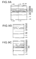
- Figs. 9A to 9C are cross-sectional views of a semiconductor laser device as the ninth embodiment of the present invention.
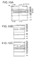
- Figs. 10A to 10C are cross-sectional views of a semiconductor laser device as the tenth embodiment of the present invention.
- Fig. 1A is a sectional side view including an active region.
- Fig. 1B is a sectional view taken along the line 1B-1B, which shows the central portion of the semiconductor laser device in the direction perpendicular to a resonance direction thereof.
- Fig. 1C is a sectional view taken along the line 1C-1C, which is the sectional view in the vicinity of an end face of the semiconductor laser device in the direction perpendicular to the resonance direction thereof.
- a first embodiment of the present invention is shown in Figs. 1A to 1C, and the structure of the semiconductor laser device of this embodiment will be described together with manufacturing processes for manufacturing the semiconductor laser device.
- a n-type GaAs substrate 101 laminated are an n-type Ga 1-z1 Al z1 As cladding layer 102 (0.57 ⁇ z1 ⁇ 0.8), an n-type or i-type In 0.49 Ga 0.51 P lower optical waveguide layer 103, an i-type In x1 Ga 1-x1 As 1-y1 P y1 lower barrier layer 104 (0 ⁇ x1 ⁇ 0.3, 0 ⁇ y1 ⁇ 0.6), an In x3 Ga 1-x3 As 1-y3 P y3 compressive strain quantum well active layer 105 (0.49y3 ⁇ x3 ⁇ 0.4, 0 ⁇ y3 ⁇ 0.1), an i-type In x1 Ga 1-x1 As 1-y1 P y1 upper barrier layer 106 having a film thickness of about 5 nm, and an In 0.49 Ga 0.51 P cap layer 107 having
- Resist is coated on the cap layer 107.
- a removal process is performed on the resist so as to form stripe-shaped portions having a width of about 40 ⁇ m at a predetermined cycle of a resonator length, which extend in a direction expressed by the following formula.
- the In 0.49 Ga 0.51 P cap layer 107 is etched by hydrochloric acid etchant using this resist as a mask, so as to expose the In x1 Ga 1-x1 As 1-y1 P y1 upper barrier layer 106.
- etching is automatically stopped immediately before the etching progresses to the upper surface of the In x1 Ga 1-x1 As 1-y1 P y1 upper barrier layer 106.
- the resist is removed, and etching is performed by use of sulfuric acid etchant until the In 0.49 Ga 0.51 P lower optical waveguide layer 103 is exposed.
- the etching is automatically stopped immediately before the etching progresses to the upper surface of the In 0.49 Ga 0.51 P lower optical waveguide layer 103.
- the stripe-shaped portions (the portions in the vicinity of the end face) of the active layer 105, the lower and upper barrier layers 104 and 106 and the In 0.49 Ga 0.51 P cap layer 107, which have a width of 40 ⁇ m and include a setting position of a resonator end, are removed.
- a p-type or i-type In 0.49 Ga 0.51 P upper optical waveguide layer 108 is grown so as to bury the removed portions in the vicinity of the end face.
- a p-type Ga 1-z1 Al z1 As first cladding layer 109 a p-type In 0.49 Ga 0.51 P first etching stop layer 110 having a film thickness of about 10 nm, a GaAs second etching stop layer 111 having a film thickness of about 10 nm, an n-type In 0.5 (Ga 1-z2 Al z2 ) 0.5 P current confinement layer 112 (0.2 ⁇ z2 ⁇ 1), an n-type In 0.49 Ga 0.51 P cap layer 113 and a GaAs layer (not shown).
- stripe-shaped regions of the resist are removed in a ⁇ 011> direction perpendicular to the stripe-shaped portions already removed.
- the stripe-shaped regions of this resist correspond to a current injection opening having a width of about 1 ⁇ m to 3 ⁇ m.
- Stripe-shaped portions of the GaAs cap layer exposed from the resist, which correspond to the current injection opening, are removed by sulfuric acid etchant using the resist as a mask. At this time, the etching is automatically stopped immediately before the etching progresses to the upper surface of the In 0.49 Ga 0.51 P cap layer 113.
- the resist is removed, stripe-shaped portions of the In 0.49 Ga 0.51 P cap layer 113 exposed on the stripe-shaped portions of the GaAs cap layer are removed by hydrochloric acid etchant using the GaAs cap layer as a mask, and hence the current injection opening is formed.
- stripe-shaped portions of the n-type In 0.5 (Ga 1-z2 Al z2 ) 0.5 P current confinement layer 112 are removed, thus forming the current injection opening.
- the GaAs cap layer used as the mask is removed by sulfuric acid etchant and simultaneously stripe-shaped portions of the GaAs second etching stop layer are removed, thus forming the current injection opening.
- a p-type Ga 1-z1 Al z1 As second cladding layer 115 and a p-type GaAs contact layer 116 are grown, and a p electrode 117 is formed on the contact layer 116.
- the substrate 101 is polished and an n electrode is formed on the polished surface. From the p-type first cladding layer 109 to the p-type second cladding layer 115 collectively constitute a p-type cladding layer (a cladding layer of the second conductive type) 120.
- a high reflectance coating is provided on one of resonator surfaces formed by cleaving a sample at a position where the resonator end face is set, and a low reflectance coating is provided on the other resonator surface thereof. Then, the above construction is formed into a chip, thus completing the semiconductor laser device.
- the p-type cladding layer 109 shall have a film thickness with which the semiconductor laser device can realize a high output power in a fundamental transverse mode oscillation, and the p-type first and second cladding layers 109 and 115 shall have compositions with which the semiconductor laser device can realize a high output power in the fundamental transverse mode.
- the film composition is set to a value so that an equivalent refractive index step difference is in a range from 1.5 ⁇ 10 - 3 to 7 ⁇ 10 -3 .
- the composition of each cladding layer may satisfactorily be one having a band gap larger than that of the optical waveguide layer.
- each cladding layer As a material of each cladding layer, InGaAlP series material or InGaAlAsP series material which is lattice-matched with the GaAs substrate 101 can be employed in addition to the foregoing GaAlAs. Furthermore, the active layer may be a multiple quantum well.
- a GaAs cap layer having a film thickness of about 10 nm is formed on the In 0.49 Ga 0.51 P cap layer 107, and resist is coated on the GaAs cap layer.
- a removal process is performed on the resist so as to form stripe-shaped portions having a width of about 40 ⁇ m at a predetermined cycle of a resonator length, which extend in a direction expressed by the following formula.
- the GaAs cap layer is removed to be stripe-shaped by sulfuric acid etchant using this resist as a mask.
- the In 0.49 Ga 0.51 P cap layer 107 is removed by hydrochloric acid etchant using the GaAs cap layer as a mask.
- an etching step is performed with sulfuric acid etchant until the entire GaAs cap layer is removed and simultaneously the In 0.49 Ga 0.51 P lower optical waveguide layer 103 is exposed.
- FIG. 2A is a sectional side view including an active region.
- Fig. 2B is a sectional view taken along the line 2B-2B, which shows the central portion of the semiconductor laser device in the direction perpendicular to a resonance direction thereof.
- Fig. 2C is a sectional view taken along the line 2C-2C, which is the sectional view in the vicinity of an end face of the semiconductor laser device in the direction perpendicular to the resonance direction thereof. Only differences of a semiconductor laser device from that of the first embodiment will be described. The same layers as in the first embodiment are denoted by the same reference numerals, and detailed descriptions for them are omitted.
- Steps performed until the p-type GaAs contact layer 116 is formed are identical to the manufacturing steps of the first embodiment.
- the p-type GaAs contact layer 116 is removed in the stripe-shaped region corresponding to a region (the portion in the vicinity of the end face) where the active layer 105 is removed.
- the portions where the p-type GaAs contact layer 116 is removed are covered with the insulating film 119.
- the insulating film 119 is formed in the portion in the vicinity of the end face instead of the contact layer 116.
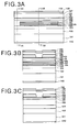
- FIG. 3A is a sectional side view including an active region.
- Fig. 3B is a sectional view taken along the line 3B-3B, which shows the central portion of the semiconductor laser device in the direction perpendicular to a resonance direction thereof.
- Fig. 3C is a sectional view taken along the line 3C-3C, which is the sectional view in the vicinity of an end face of the semiconductor laser device in the direction perpendicular to the resonance direction thereof. Descriptions of a structure of a semiconductor laser device of the third embodiment will be made together with manufacturing steps thereof.
- Resist is coated on the In 0.49 Ga 0.51 P cap layer 129.
- a removal process is performed on the resist so as to form stripe-shaped portions having a width of about 40 ⁇ m at a predetermined cycle of a resonator length, which extend in a direction expressed by the following formula.
- the In 0.49 Ga 0.51 P cap layer 129 is etched by hydrochloric acid etchant using this resist as a mask.
- the In x2 Ga 1-x2 As 1-y2 P y2 upper barrier layer 128 is exposed.
- etching is automatically stopped immediately before the etching progresses to the upper surface of the In x2 Ga 1-x2 As 1-y2 P y2 upper barrier layer 128.
- the resist is removed, and etching is performed by use of sulfuric acid etchant until the In 0.49 Ga 0.51 P lower optical waveguide layer 123 is exposed.
- the etching is automatically stopped immediately before the etching progresses to the upper surface of the In 0.49 Ga 0.51 P lower optical waveguide layer 123.
- the stripe-shaped portions (the portions in the vicinity of the end face) of the active layer 126, the lower and upper stretch barrier layers 125 and 127, the lower and upper barrier layers 124 and 128, and the In 0.49 Ga 0.51 P cap layer 109, which have a width of 40 ⁇ m and include a setting position of a resonator end, are removed.
- a p-type or i-type In 0.49 Ga 0.51 P upper optical waveguide layer 130 is grown so as to bury the removed portions in the vicinity of the end face.
- formed are a p-type Ga 1-z1 Al z1 As first cladding layer 131, a p-type In 0.49 Ga 0.51 P first etching stop layer 132 having a film thickness of about 10 nm, a GaAs second etching stop layer 133 having a film thickness of about 10 nm, an n-type In 0.5 (Ga 1-z2 Al z2 ) 0.5 P current confinement layer 134 (0.2 ⁇ z2 ⁇ 1) and an n-type In 0.49 Ga 0.51 P cap layer 135.
- the resist is coated. Then, stripe-shaped regions of the resist are removed in a ⁇ 011> direction perpendicular to the stripe-shaped portions already removed.
- the stripe-shaped regions of this resist correspond to a current injection opening having a width of about 1 ⁇ m to 3 ⁇ m.
- the stripe-shaped portions of the n-type In 0.49 Ga 0.51 P cap layer 135 and the n-type In 0.5 (Ga 1-z2 Al z2 ) 0.5 P current confinement layer 134 are removed using this resist as a mask. At this time, the etching is automatically stopped immediately before the etching progresses to the upper surface of the GaAs second etching stop layer 133.
- the resist is removed, and stripe-shaped portions of the GaAs second etching stop layer 133 are removed by sulfuric acid etchant. Thus, a current injection opening is formed. Subsequently, a p-type Ga 1-z1 Al z1 As second cladding layer 137 and a p-type GaAs contact layer 138 are grown. The p electrode 139 is formed on the contact layer 138. Thereafter, the substrate 121 is polished, and an n electrode 140 is formed on the polished surface.
- a high reflectance coating is provided on one of resonator surfaces formed by cleaving a sample at a position where the resonator end face is set, and a low reflectance coating is provided on the other resonator surface thereof. Then, the above construction is formed into a chip, thus completing the semiconductor laser device.
- the p-type first cladding layer 131 shall have a film thickness and the p-type second cladding layer 137 shall have a composition, whereby the semiconductor laser device can realize a high output power in a fundamental transverse mode oscillation.
- the film thickness and the composition are set so that an equivalent refractive index step difference is in a range from 1.5 5 ⁇ 10 -3 to 7 ⁇ 10 -3 .
- the composition of each cladding layer may satisfactorily be one having a band gap larger than that of the optical waveguide layer.
- each cladding layer As a material of each cladding layer, InGaAlP series material or InGaAlAsP series material which is lattice-matched with the GaAs substrate 101 can be employed in addition to the foregoing GaAlAs. Furthermore, though the active layer may be a multiple quantum well, an absolute value of a sum of products of a strain quantity and a film thickness of the tensile strain barrier layer and the compressive strain active layer should be set to 0.3 nm or less.
- FIG. 4A is a sectional side view including an active region.
- Fig. 4B is a sectional view taken along the line 4B-4B, which shows the central portion of the semiconductor laser device in the direction perpendicular to a resonance direction thereof.
- Fig. 4C is a sectional view taken along the line 4C-4C, which is the sectional view in the vicinity of an end face of the semiconductor laser device in the direction perpendicular to the resonance direction thereof.
- an n-type Ga 1-z1 Al z1 As cladding layer 142 (0.57 ⁇ z1 ⁇ 0.8)
- an n-type or i-type In 0.49 Ga 0.51 P lower optical waveguide layer 143 an i-type In x1 Ga 1-x1 As 1-y1 P y1 lower barrier layer 144 (0 ⁇ x1 ⁇ 0.3, 0.1 ⁇ y1 ⁇ 0.6)
- an In x3 Ga 1-x3 As 1-y3 P y3 compressive strain quantum well active layer 145 (0.49y3 ⁇ x3 ⁇ 0.4, 0 ⁇ y3 ⁇ 0.1
- an i-type In x1 Ga 1-x1 As 1-y1 P y1 upper barrier layer 146 having a film thickness of about 5 nm
- an In 0.49 Ga 0.51 P cap layer 147 having a film thickness of about 10 nm by an organometallic vapor phase growth method.
- Resist is coated on the cap layer 147.
- a removal process is performed on the resist so as to form stripe-shaped portions having a width of about 40 ⁇ m at a predetermined cycle of a resonator length, which extend in a direction expressed by the following formula.
- the In 0.49 Ga 0.51 P cap layer 147 is etched by hydrochloric acid etchant using this resist as a mask, so as to expose the In x1 Ga 1-x1 As 1-y1 P y1 upper barrier layer 146.
- the etching is automatically stopped immediately before the etching progresses to the upper surface of the In x1 Ga 1-x1 As 1-y1 P y1 upper barrier layer 146.
- the resist is removed, and etching is performed by use of sulfuric acid etchant until the In 0.49 Ga 0.51 P lower optical waveguide layer 143 is exposed.
- the etching is automatically stopped immediately before the etching progresses to the upper surface of the In 0.49 Ga 0.51 P lower optical waveguide layer 143.
- the stripe-shaped portions (the portions in the vicinity of the end face) of the active layer 145, the lower and upper barrier layers 144 and 146 and the In 0.49 Ga 0.51 P cap layer 147, which have a width of 40 ⁇ m and include a setting position of a resonator end, are removed.
- a p-type or i-type In 0.49 Ga 0.51 P upper optical waveguide layer 148, a GaAs etching stop layer 149 having a film thickness of about 10 nm, an n-type In 0.5 (Ga 1-z2 Al z2 ) 0.5 P current confinement layer 150 (0.2 ⁇ z2 ⁇ 1), an n-type In 0.49 Ga 0.51 P cap layer 151 and a GaAs cap layer are formed so as to bury the removed portions in the vicinity of the end face.
- the resist is coated, and the regions of the resist having a width of 1 ⁇ m to 3 ⁇ m in a ⁇ 011> direction perpendicular to the already removed stripe-shapes portions are removed, and stripe-shaped portions of the GaAs cap layer 152 are removed by sulfuric acid etchant using this resist as a mask, thus forming a current injection opening.
- the etching is automatically stopped immediately before the etching progresses to the upper surface of the In 0.49 Ga 0.51 P cap layer 151.
- the resist is removed, and the stripe-shaped portions of the In 0.49 Ga 0.51 P cap layer 151 and the n-type In 0.5 (Ga 1-z2 Al z2 ) 0.5 P current confinement layer 150 are removed by hydrochloric acid etchant.
- a current injection opening is formed.
- the GaAs cap layer used as the mask is removed, and the stripe-shaped portions of the GaAs etching stop layer 149 are removed, thus forming a current injection opening.
- a p-type Ga 1-z1 Al z1 As second cladding layer 153 and a p-type GaAs contact layer 154 are grown.
- a p electrode 155 is formed on the contact layer 154.
- the substrate 141 is polished, and an n electrode 156 is formed on the polished surface.
- a high reflectance coating is provided on one of resonator surfaces formed by cleaving a sample at a position where the resonator end face is set, and a low reflectance coating is provided on the other resonator surface thereof. Then, the above construction is formed into a chip, thus completing the semiconductor laser device.
- the upper optical waveguide layer 148 shall have a value and the p-type second cladding layer 153 shall have a composition, whereby the semiconductor laser device can realize a high output power in a fundamental transverse mode oscillation.
- the film thickness and the composition are set so that an equivalent refractive index step difference is in a range from 1.5 ⁇ 10 -3 to 7 ⁇ 10 -3 .
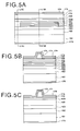
- FIG. 5A is a sectional side view including an active region.
- Fig. 5B is a sectional view taken along the line 5B-5B, which shows the central portion of the semiconductor laser device in the direction perpendicular to a resonance direction thereof.
- Fig. 5C is a sectional view taken along the line 5C-5C, which is the sectional view in the vicinity of an end face of the semiconductor laser device in the direction perpendicular to the resonance direction thereof.
- an n-type Ga 1-z1 Al z1 As cladding layer 162 (0.57 ⁇ z1 ⁇ 0.8)
- an n-type or i-type In 0.49 Ga 0.51 P lower optical waveguide layer 163 having a film thickness of about 5 nm
- an i-type In x1 Ga 1-x1 As 1-y1 P y1 lower barrier layer 164 (0 ⁇ x1 ⁇ 0.3, 0 ⁇ y1 ⁇ 0.6) having a film thickness of about 10 nm
- an In x3 Ga 1-x3 As 1-y3 P y3 compressive strain quantum well active layer 165 (0.49y3 ⁇ x3 ⁇ 0.4, 0 ⁇ y3 ⁇ 0.1
- an i-type In x1 Ga 1-x1 As 1-y1 P y1 upper barrier layer 166 having a film thickness of about 10 nm
- an In 0.49 Ga 0.51 AsP cap layer 167 having a film thickness of about 5 nm by an organometallic vapor phase growth method.
- Resist is coated on the cap layer 167.
- a removal process is performed on the resist so as to form stripe-shaped portions having a width of about 40 ⁇ m at a predetermined cycle of a resonator length, which extend in a direction expressed by the following formula.
- the In 0.49 Ga 0.51 P cap layer 167 is etched by hydrochloric acid etchant using this resist as a mask, so as to expose the In x1 Ga 1-x1 As 1-y1 P y1 upper barrier layer 166.
- the etching is automatically stopped immediately before the etching progresses to the upper surface of the In x1 Ga 1-x1 As 1-y1 P y1 upper barrier layer 166.
- the resist is removed, and etching is performed by use of sulfuric acid etchant until the In 0.49 Ga 0.51 P lower optical waveguide layer 163 is exposed.
- the etching is automatically stopped immediately before the etching progresses to the upper surface of the In 0.49 Ga 0.51 P lower optical waveguide layer 163.
- the stripe-shaped portions (the portions in the vicinity of the end face) of the active layer 165, the lower and upper barrier layers 164 and 166 and the In 0.49 Ga 0.51 P cap layer 167, which have a width of 40 ⁇ m and include a setting position of a resonator end, are removed.
- an insulating film (not shown) is formed, and the insulating film is removed so that stripe-shaped portions having a width of about 1 ⁇ m to 3 ⁇ m are left in a ⁇ 011> direction.
- Both sides of the stripe-shaped portions of the p-type GaAs contact layer 172 and the p-type Ga 1-z1 Al z1 As second cladding layer 171 are removed by sulfuric acid etchant using this insulating film as a mask, thus forming a ridge.
- an insulating film 173 is formed, and a current injection opening is formed only in an upper portion of the ridge by an ordinary lithography technique.
- a p electrode 174 is formed so as to cover the current injection opening.
- the substrate 161 is polished, and an n electrode 175 is formed on the polished surface.
- a high reflectance coating is provided on one of resonator surfaces formed by cleaving a sample at a position where the resonator end face is set, and a low reflectance coating is provided on the other resonator surface thereof. Then, the above construction is formed into a chip, thus completing the semiconductor laser device.
- the p-type second cladding layer shall have a film thickness with which the semiconductor laser device can realize a high output power in a fundamental transverse mode oscillation. Specifically, the film thickness is set so that an equivalent refractive index step difference is in a range from 1.5 ⁇ 10 -3 to 7 ⁇ 10 -3 .
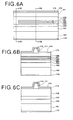
- FIG. 6A is a sectional side view including an active region.
- Fig. 6B is a sectional view taken along the line 6B-6B, which shows the central portion of the semiconductor laser device in the direction perpendicular to a resonance direction thereof.
- Fig. 6C is a sectional view taken along the line 6C-6C, which is the sectional view in the vicinity of an end face of the semiconductor laser device in the direction perpendicular to the resonance direction thereof. Only differences of a semiconductor laser device from that of the fifth embodiment will be described. The same layers as those in the fifth embodiment are denoted by the same reference numerals, and detailed descriptions for them are omitted.
- a semiconductor laser device of the sixth embodiment of the present invention does not comprise the p-type Ga 1-z1 Al z1 As first cladding layer 169, the p-type In 0.49 Ga 0.51 P etching stop layer 170 formed on the upper optical waveguide layer 168 in the fifth embodiment.
- the p-type cladding layer part may comprise only one p-type cladding layer.
- the upper optical waveguide layer 168 shall have a film thickness with which the semiconductor laser device can realize a high output power in a fundamental transverse mode. Specifically, the film thickness is set so that an equivalent refractive index step difference is in a range from 1.5 ⁇ 10 -3 to 7 ⁇ 10 -3 .
- the composition of the In x3 Ga 1-x3 As y3 P 1-y3 compressive strain active layer is controlled in a range of 0.49y3 ⁇ x3 ⁇ 0.4 and 0 ⁇ y3 ⁇ 0.1, whereby an oscillation wavelength can be controlled in a range of 900 ⁇ 1200 (nm).
- a molecular beam epitaxial growth method using a solid or a gaseous raw material may be employed.
- the suffixes x, y and z that are not particularly range-specified have values ranging from 0 to 1, and they are properly decided depending on lattice match conditions, lattice unmatched conditions, a scale of a band gap and a magnitude of a refractive index regarding an oscillation wavelength.
- n-type GaAs substrate was used, a p-type GaAs substrate may be also employed. In this case, layers having opposite conductivity type to those of the layers used in the semiconductor laser devices in the above described embodiments may be laminated.
- a semiconductor laser element can generate a laser beam with a high level optical output while maintaining a fundamental transverse mode.
- the present invention is effective not only in laser elements that oscillate a fundamental transverse mode, but in semiconductor laser elements that oscillate in a multi-mode having an oscillation region width of 3 ⁇ m or wider, and thus a highly reliable semiconductor laser element of a multi-mode oscillation with low-noise and high-output oscillation can be obtained.
- FIG. 7 to 10 Embodiments of the present invention are explained in detail using Figs. 7 to 10.
- (A) is a sectional side view cut at a surface including an active region
- (B) is a cross-sectional view taken along the line B-B(the cross-sectional view in the vicinity of an end face of the semiconductor laser device in the direction perpendicular to the resonance direction thereof)
- (C) is a cross-sectional view taken along the line C-C(the central portion of the semiconductor laser device in the direction perpendicular to a resonance direction thereof).
- the seventh embodiment of the present invention is shown in Fig. 7.
- the present semiconductor laser device comprises an n-type GaAs buffer layer 222, an n-type Al z1 Ga 1-z1 As lower cladding layer 223 (0.57 ⁇ z1 ⁇ 0.8), an n-or i-type In 0.49 Ga 0.51 P lower optical waveguide layer 224, an i-type In x3 Ga 1-x3 As 1-y3 P y3 lower barrier layer 225 (0 ⁇ x3 ⁇ 0.3,0.1 ⁇ y3 ⁇ 0.6), a compressive strain In x1 Ga 1-x1 As 1-y1 P y1 quantum well active layer 226 (0 ⁇ x1 ⁇ 0.4,0 ⁇ y1 ⁇ 0.1), an i-type In x3 Ga 1-x3 As 1-y3 P y3 upper barrier layer 227 (0 ⁇ x3 ⁇ 0.3,0.1 ⁇ y3 ⁇ 0.6), an In 0.49 Ga 0.51 P first cap layer 228, a
- the contact layer 236 and the p-side electrode 237 formed on the upper surface of the contact layer 236 are not formed in a region which is up to about 20 ⁇ m inwardly from an end face of a resonator (a portion in the vicinity of the end face).
- the contact layer 236 and the electrode 237 are structured not to be formed on the portion in the vicinity of the end face, so that the current injection to the portion in the vicinity of the end face is suppressed, making it possible to restrain occurrence of nonluminous recombination and to suppress occurrence of COMD on the end face.
- the electrode 237 may not always have the same size as that of the contact layer 236, and may be extended toward the end face from the contact layer 236.
- the eighth embodiment of the present invention is shown in Fig. 8.
- the present semiconductor laser device has substantially the same layer structure as that of the seventh embodiment, but it is different from the seventh embodiment in the point that an insulation film 239 is formed on the portion which is on the upper surface of the upper cladding layer 235 and which is the portion in the vicinity of the end face where no contact layer 236 is formed and the point that the p-side electrode 237 is formed on the contact layer 236 and insulation film 239. Similar to the above-mentioned case, this case can obtain an effect that controls the current injection to the portion in the vicinity of the end face so as to suppress occurrence of nonluminous recombination on the end face.
- the ninth embodiment of the present invention is shown in Fig. 9.
- the present semiconductor laser device has substantially the same layer structure as that of the seventh embodiment, but it is different from the seventh embodiment in the point that the layers including the lower barrier layer 225 to the first cap layer 228 are formed only inwardly from the position away from the end faces of the resonator by a predetermined distance and the upper first optical waveguide layer is buried in the portion in the vicinity of the end face, which is from the edge portions of these layers to the end face of the resonator and the point that the contact layer 236 is formed on the entire surface of the upper cladding layer 235, and the p-side electrode 237 of the contact layer 236 is also formed on the entire surface of the laminated surface.
- the contact layer 236 and the p-side electrode 237 are structured to be formed on the entire surface of the laminated surface, by providing the so-called window structure in which the portions of the lower barrier layer 225 to the first cap layer 228 in the vicinity of the end faces are removed and an optical waveguide layer with a band gap larger than that of the active layer is buried in the removed portions, it is possible to control absorption of a laser beam in the vicinity of the end portion and to suppress occurrence of COMD.
- an n-type GaAs buffer layer 222, an n-type Al z1 Ga 1-z1 As lower cladding layer 223 (0.57 ⁇ z1 ⁇ 0.8), an n-or i-type In 0.49 Ga 0.51 P lower optical waveguide layer 224, an i-type In x3 Ga 1-x3 As 1-y3 P y3 lower barrier layer 225 (0 ⁇ x3 ⁇ 0.3,0.1 ⁇ y3 ⁇ 0.6), a compressive strain In x1 Ga 1-x1 As 1-y1 P y 1 quantum well active layer 226 (0 ⁇ x1 ⁇ 0.4,0 ⁇ y1 ⁇ 0.1), an i-type In x3 Ga 1-x3 As 1-y3 P y3 upper barrier layer 227 (0 ⁇ x3 ⁇ 0.3,0.1 ⁇ y3 ⁇ 0.6), and an In 0.49 Ga 0.51 P first cap layer 228 are
- the In 0.49 Ga 0.51 P first cap layer 228 is etched by hydrochloric acid etchant using this resist as a mask, so as to expose the i-type In x3 Ga 1-x3 As 1-y3 P y3 upper barrier layer 227.
- etching is automatically stopped at the upper surface of the i-type In x3 Ga 1-x3 As 1-y3 P y3 upper barrier layer 227.
- the resist is removed, and etching is performed by use of sulfuric acid etchant until the In 0.49 Ga 0.51 P lower optical waveguide layer 224 is exposed.
- the etching is automatically stopped at the upper surface of the In 0.49 Ga 0.51 P lower optical waveguide layer 224.
- the stripe-shaped portions (the portions in the vicinity of the end face) of the active layer 226, the lower and upper barrier layers 225 and 227 and the first cap layer 228, which have a width of 40 ⁇ m and which include a setting position of a resonator end face, are removed.
- a p- or i-type In 0.49 Ga 0.51 P upper first optical waveguide layer 229 is grown so as to bury the removed portions in the vicinity of the end face.
- a p-type GaAs etching stop layer 230 (thickness of about 10 nm)
- an n-type In 0.49 (Al z2 Ga 1-z2 ) 0.51 P current confinement layer 231
- an n-type In 0.49 Ga 0.51 P second cap layer 232 (thickness of about 10 nm)
- an n-type GaAs third cap layer is coated with resist.
- the resist on stripe-shaped regions which correspond to a current injection opening having a width of about 1 ⁇ m to 3 ⁇ m, is removed in a ⁇ 011> direction perpendicular to the stripe-shaped portions already removed.
- Stripe-shaped portions of the n-type GaAs third cap layer exposed to the opening of the resist, which correspond to the current injection opening, are removed by sulfuric acid etchant using the resist as a mask. At this time, the etching is automatically stopped at the upper surface of the n-type In 0.49 Ga 0.51 P second cap layer 232.
- the resist is removed, stripe-shaped portions of the n-type In 0.49 Ga 0.51 P second cap layer 232 exposed to the opening of the third cap layer are removed by hydrochloric acid etchant using the n-type GaAs third cap layer as a mask, and sequentially the strip-shaped portions of the n-type In 0.49 (Al z2 Ga 1-z2 ) 0.51 P current confinement layer 231 are removed so as to form a current injection opening.
- the etching is automatically stopped at the n-type GaAs etching stop layer 230.
- the n-type GaAs etching stop layer 230 exposed to the opening portion is removed by sulfuric acid etchant and the residual n-type GaAs third cap layer is removed.
- a p-type In 0.49 Ga 0.51 P upper second optical waveguide layer 234, a p-type Al z1 Ga 1-z1 As upper cladding layer 235 (0.57 ⁇ z1 ⁇ 0.8) and a p-type GaAs contact layer 236 are formed. Thereafter, a p-side electrode 237 is formed on the contact layer 236, the substrate 221 is polished, and an n-side electrode 238 is formed on the polished surface.
- a high reflectance coating is provided on one of resonator surfaces formed by cleaving a sample at a position where the resonator end face is set, and a low reflectance coating is provided on the other resonator surface thereof. Then, the above construction is formed into a chip, thus completing the semiconductor laser device.
- the thickness of the p-type In 0.49 Ga 0.51 P upper second optical waveguide layer 234 and the composition and thickness of the n-type In 0.49 (Al z2 Ga 1-z2 ) 0.51 P current confinement layer 231 are set in a condition that a fundamental transverse mode oscillation can be maintained up to high power, specifically, an equivalent refractive index step difference between the stripe shaped regions and the current confinement layer region is in a range from 1.5 ⁇ 10 - 3 to 7.0 ⁇ 10 -3 .
- an In x2 Ga 1-x2 As 1-y2 P y2 strain compensation layer (0 ⁇ x2 ⁇ 0.49y2, 0 ⁇ y2 ⁇ 0.5), which has a band gap larger than that of the active layer and which has tensile strain stress, may be formed between the active layer and the barrier layer.
- the sum of the product of the strain quantity and the thickness of the compressive strain active layer and the product of the strain quantity and the thickness of the tensile strain compensation layer is set to be within 0.3 nm.
- GaAs etching stop layer 230 In 0.49 Ga 0.51 P second cap layer 232 and GaAs third cap layer, either of n-type or p-type may be used.
- this embodiment uses In 0.49 Ga 0.51 P as upper second optical waveguide layer 234, the same effect can be obtained if Al z3 Ga 1-z3 As (0.50 ⁇ z3 ⁇ 0.54) having substantially the same refractive index as that of In 0.49 Ga 0.51 P is used.
- the semiconductor laser device of this embodiment is one that has the structure in which the end face current injection control structure of the eighth embodiment and the window structure of the ninth embodiment are combined and that has higher reliability in which a current injection to a window region is greatly suppressed so as to increase a window effect.
- the manufacturing method of the present semiconductor laser device After forming the layers up to the p-type GaAs contact layer 236 by the same method as that of the manufacturing method of the ninth embodiment, the p-type GaAs contact layer 236 of the stripe-shaped region in the vicinity of the end face, which corresponds to the region where the active layer is removed, is eliminated. The removed portion is covered with an insulation film 239. Thereafter, a p-side electrode 237 is formed thereon, and the substrate 221 is polished so as to form an n-side electrode 238 on the polished surface. Thereafter, a high reflectance coating and a low reflectance coating are provided on the resonator surfaces formed by cleaving a sample, and then the above construction is formed into a chip, thus completing the semiconductor laser device.
- the structure having the end face current injection control structure of the seventh embodiment may be used.
- a method in which the p-type GaAs contact layer 236 of the stripe region corresponding to the region where the active layer is removed is eliminated, thereafter the p-side electrode 237 is formed thereon along the p-type GaAs contact layer 236.
- the end face current injection control structure may be provided onto both low reflectance coating side and high reflectance coating side or only one of the low reflectance coating side and high reflectance coating side. Moreover, even if the window structure is formed on only one end face, a constant effect that suppresses COMD can be obtained.
- In 0.49 (Ga 1-z4 Al z4 ) 0.51 P layers (0.1 ⁇ z4 ⁇ z2) may be used as lower and upper cladding layers.
- molecular beam epitaxy using solid or gas raw material may be used as growth of each semiconductor layer.
- the GaAs substrate with n-type conductivity was described.
- a GaAs substrate with p-type conductivity may be also employed.
- all conductivities of layers may be changed to be opposite to those of the layers used in the semiconductor laser devices in the above-described embodiments.
- composition ratio of the In x1 Ga 1-x1 As 1-y1 P y1 active layer is controlled in a range of 0 ⁇ x1 ⁇ 0.4, 0 ⁇ y1 ⁇ 0.1, making it possible to complete a semiconductor laser device having a peak oscillation wavelength in a range of 900 ⁇ ⁇ ⁇ 1200 (nm).
- the quantum well in the active layer was a single layer in the aforementioned embodiments.
- a structure having a multiple quantum well in which quantum wells are laminated in a multilayer manner there may be used a structure in which a layer, which is made of the same material as that of the optical waveguide layer or the barrier layer, is interposed between the respective quantum well layers.
- a refractive index waveguide type semiconductor laser device which has a stripe width of 4 ⁇ m or more and which provides a multimode oscillation.
- its equivalent refractive index step difference ⁇ N is set to 2 ⁇ 10 -3 or more.
- the above-structured semiconductor laser device with the wide stripe has a low noise characteristic and can be used as a semiconductor laser device with high power required for solid laser excitation and the like.
- the semiconductor laser device structure of the present invention can be used in fabricating not only the semiconductor laser devices with a refractive index waveguide mechanism but also the semiconductor laser devices having a diffraction lattice, or optical integrated circuits.
Landscapes
- Physics & Mathematics (AREA)
- Condensed Matter Physics & Semiconductors (AREA)
- General Physics & Mathematics (AREA)
- Electromagnetism (AREA)
- Optics & Photonics (AREA)
- Semiconductor Lasers (AREA)
Applications Claiming Priority (6)
| Application Number | Priority Date | Filing Date | Title |
|---|---|---|---|
| JP2001158404 | 2001-05-28 | ||
| JP2001158404 | 2001-05-28 | ||
| JP2001172610A JP2003051641A (ja) | 2001-05-28 | 2001-06-07 | 半導体レーザ装置および製造方法 |
| JP2001172610 | 2001-06-07 | ||
| JP2001256234 | 2001-08-27 | ||
| JP2001256234A JP2003069148A (ja) | 2001-08-27 | 2001-08-27 | 半導体レーザ素子 |
Publications (2)
| Publication Number | Publication Date |
|---|---|
| EP1263100A2 true EP1263100A2 (de) | 2002-12-04 |
| EP1263100A3 EP1263100A3 (de) | 2005-02-09 |
Family
ID=27346792
Family Applications (1)
| Application Number | Title | Priority Date | Filing Date |
|---|---|---|---|
| EP02011749A Withdrawn EP1263100A3 (de) | 2001-05-28 | 2002-05-27 | Halbleiterlaser und dessen Herstellungsverfahren |
Country Status (1)
| Country | Link |
|---|---|
| EP (1) | EP1263100A3 (de) |
Cited By (1)
| Publication number | Priority date | Publication date | Assignee | Title |
|---|---|---|---|---|
| DE102004010260A1 (de) * | 2004-03-03 | 2005-09-22 | Fraunhofer-Gesellschaft zur Förderung der angewandten Forschung e.V. | Verfahren zur Herstellung eines Halbleiterlasers mit einer aluminiumhaltigen Aktivschicht und mit dem Verfahren hergestellter Halbleiterlaser mit Rippenwellenleiter |
Family Cites Families (3)
| Publication number | Priority date | Publication date | Assignee | Title |
|---|---|---|---|---|
| DE69725783T2 (de) * | 1996-06-17 | 2004-07-29 | Fuji Photo Film Co., Ltd., Minami-Ashigara | Halbleiterlaser |
| FR2788172B1 (fr) * | 1998-12-30 | 2001-10-05 | Thomson Csf | Procede de realisation de structures laser de puissance a miroirs non absorbants et structures ainsi obtenues |
| JP2002141610A (ja) * | 2000-10-31 | 2002-05-17 | Fuji Photo Film Co Ltd | 半導体レーザ素子およびその製造方法 |
-
2002
- 2002-05-27 EP EP02011749A patent/EP1263100A3/de not_active Withdrawn
Cited By (2)
| Publication number | Priority date | Publication date | Assignee | Title |
|---|---|---|---|---|
| DE102004010260A1 (de) * | 2004-03-03 | 2005-09-22 | Fraunhofer-Gesellschaft zur Förderung der angewandten Forschung e.V. | Verfahren zur Herstellung eines Halbleiterlasers mit einer aluminiumhaltigen Aktivschicht und mit dem Verfahren hergestellter Halbleiterlaser mit Rippenwellenleiter |
| DE102004010260B4 (de) * | 2004-03-03 | 2008-07-17 | Fraunhofer-Gesellschaft zur Förderung der angewandten Forschung e.V. | Verfahren zur Herstellung eines Halbleiterlasers mit einer aluminiumhaltigen Aktivschicht und mit dem Verfahren hergestellter Halbleiterlaser mit Rippenwellenleiter |
Also Published As
| Publication number | Publication date |
|---|---|
| EP1263100A3 (de) | 2005-02-09 |
Similar Documents
| Publication | Publication Date | Title |
|---|---|---|
| US6580738B2 (en) | High-power semiconductor laser device in which near-edge portions of active layer are removed | |
| JPH11220224A (ja) | 半導体レーザ装置 | |
| EP0936709B1 (de) | Halbleiterlaser | |
| US6396863B1 (en) | High-power semiconductor laser device having index-guided structure with InAlGaP current confinement layer | |
| EP1220393B1 (de) | Halbleiterlaservorrichtung mit einer aktiven Schicht aus InGaAs unter Kompressionsdruck, einer Sperrschicht aus GaAsP unter Dehnungsdruck, und einem Lichtwellenleiter aus InGaP | |
| US6400743B1 (en) | High-power semiconductor laser device having current confinement structure and index-guided structure | |
| US6856636B2 (en) | Semiconductor laser device | |
| EP1211766B1 (de) | InGaAsP-Halbleiterlaser | |
| US20020044584A1 (en) | Semiconductor laser device which includes AlGaAs optical waveguide layer being formed over internal stripe groove and having controlled refractive index | |
| US6973109B2 (en) | Semiconductor laser device having strain buffer layer between compressive-strain quantum well layer and tensile-strain barrier layer | |
| US20010017871A1 (en) | High-power semiconductor laser device in which near-edge portions of active layer are removed | |
| EP1263100A2 (de) | Halbleiterlaser und dessen Herstellungsverfahren | |
| EP1304781B1 (de) | Halbleiterlaserelement mit Fensterstruktur | |
| US6795469B2 (en) | Semiconductor laser element | |
| US6600770B2 (en) | High-power semiconductor laser device having current confinement structure and index-guided structure and stably oscillating in single mode | |
| JP2001320135A (ja) | 半導体レーザ装置 | |
| JP2002204032A (ja) | 半導体レーザ素子 | |
| EP1251609B1 (de) | Hochleistungs-Halbleiterlaservorrichtung mit Fensterstruktur | |
| US6873637B2 (en) | Semiconductor laser element including optical waveguide layers which have gradually varying bandgaps so as to reduce electrical resistance at interfaces | |
| RU2272344C2 (ru) | Полупроводниковое лазерное устройство, генерирующее излучение высокой мощности (варианты), и способ его изготовления | |
| JP2003347679A (ja) | 半導体レーザ素子 | |
| JP2003023218A (ja) | 半導体レーザ素子 | |
| KR100817487B1 (ko) | 반도체 레이저 장치 | |
| JPH1197794A (ja) | 半導体レーザ装置 | |
| JP2003060312A (ja) | 半導体レーザ素子 |
Legal Events
| Date | Code | Title | Description |
|---|---|---|---|
| PUAI | Public reference made under article 153(3) epc to a published international application that has entered the european phase |
Free format text: ORIGINAL CODE: 0009012 |
|
| AK | Designated contracting states |
Kind code of ref document: A2 Designated state(s): AT BE CH CY DE DK ES FI FR GB GR IE IT LI LU MC NL PT SE TR |
|
| AX | Request for extension of the european patent |
Free format text: AL;LT;LV;MK;RO;SI |
|
| PUAL | Search report despatched |
Free format text: ORIGINAL CODE: 0009013 |
|
| RIC1 | Information provided on ipc code assigned before grant |
Ipc: 7H 01S 5/16 B Ipc: 7H 01S 5/32 A |
|
| AK | Designated contracting states |
Kind code of ref document: A3 Designated state(s): AT BE CH CY DE DK ES FI FR GB GR IE IT LI LU MC NL PT SE TR |
|
| AX | Request for extension of the european patent |
Extension state: AL LT LV MK RO SI |
|
| 17P | Request for examination filed |
Effective date: 20050705 |
|
| AKX | Designation fees paid |
Designated state(s): CH DE FR GB IT LI |
|
| RAP1 | Party data changed (applicant data changed or rights of an application transferred) |
Owner name: FUJIFILM CORPORATION |
|
| STAA | Information on the status of an ep patent application or granted ep patent |
Free format text: STATUS: THE APPLICATION IS DEEMED TO BE WITHDRAWN |
|
| 18D | Application deemed to be withdrawn |
Effective date: 20101130 |