EP1264918A1 - Méthode de plaquage électrolytique de cuivre - Google Patents
Méthode de plaquage électrolytique de cuivre Download PDFInfo
- Publication number
- EP1264918A1 EP1264918A1 EP02253891A EP02253891A EP1264918A1 EP 1264918 A1 EP1264918 A1 EP 1264918A1 EP 02253891 A EP02253891 A EP 02253891A EP 02253891 A EP02253891 A EP 02253891A EP 1264918 A1 EP1264918 A1 EP 1264918A1
- Authority
- EP
- European Patent Office
- Prior art keywords
- bath
- electrolytic copper
- copper plating
- plating
- anode
- Prior art date
- Legal status (The legal status is an assumption and is not a legal conclusion. Google has not performed a legal analysis and makes no representation as to the accuracy of the status listed.)
- Granted
Links
Images


Classifications
-
- C—CHEMISTRY; METALLURGY
- C25—ELECTROLYTIC OR ELECTROPHORETIC PROCESSES; APPARATUS THEREFOR
- C25D—PROCESSES FOR THE ELECTROLYTIC OR ELECTROPHORETIC PRODUCTION OF COATINGS; ELECTROFORMING; APPARATUS THEREFOR
- C25D3/00—Electroplating: Baths therefor
- C25D3/02—Electroplating: Baths therefor from solutions
- C25D3/38—Electroplating: Baths therefor from solutions of copper
-
- C—CHEMISTRY; METALLURGY
- C25—ELECTROLYTIC OR ELECTROPHORETIC PROCESSES; APPARATUS THEREFOR
- C25D—PROCESSES FOR THE ELECTROLYTIC OR ELECTROPHORETIC PRODUCTION OF COATINGS; ELECTROFORMING; APPARATUS THEREFOR
- C25D17/00—Constructional parts, or assemblies thereof, of cells for electrolytic coating
- C25D17/10—Electrodes, e.g. composition, counter electrode
-
- C—CHEMISTRY; METALLURGY
- C25—ELECTROLYTIC OR ELECTROPHORETIC PROCESSES; APPARATUS THEREFOR
- C25D—PROCESSES FOR THE ELECTROLYTIC OR ELECTROPHORETIC PRODUCTION OF COATINGS; ELECTROFORMING; APPARATUS THEREFOR
- C25D21/00—Processes for servicing or operating cells for electrolytic coating
- C25D21/16—Regeneration of process solutions
- C25D21/18—Regeneration of process solutions of electrolytes
-
- C—CHEMISTRY; METALLURGY
- C25—ELECTROLYTIC OR ELECTROPHORETIC PROCESSES; APPARATUS THEREFOR
- C25D—PROCESSES FOR THE ELECTROLYTIC OR ELECTROPHORETIC PRODUCTION OF COATINGS; ELECTROFORMING; APPARATUS THEREFOR
- C25D5/00—Electroplating characterised by the process; Pretreatment or after-treatment of workpieces
- C25D5/18—Electroplating using modulated, pulsed or reversing current
-
- H—ELECTRICITY
- H05—ELECTRIC TECHNIQUES NOT OTHERWISE PROVIDED FOR
- H05K—PRINTED CIRCUITS; CASINGS OR CONSTRUCTIONAL DETAILS OF ELECTRIC APPARATUS; MANUFACTURE OF ASSEMBLAGES OF ELECTRICAL COMPONENTS
- H05K3/00—Apparatus or processes for manufacturing printed circuits
- H05K3/40—Forming printed elements for providing electric connections to or between printed circuits
- H05K3/42—Plated through-holes or plated via connections
- H05K3/423—Plated through-holes or plated via connections characterised by electroplating method
Definitions
- This invention pertains to an electrolytic copper plating method. More particularly, this invention pertains to an electrolytic copper plating method that does not mar the appearance of plating and is applied to form filled via-holes.
- via-filling In recent years, a method called "via-filling" has been developed for filling the entire via-hole (or “via") in this type of build-up printed circuit board with a conductor and electrically connecting adjacent build-up printed circuit boards.
- This method is effective for miniaturizing and increasing the density of printed circuit boards by enabling the effective surface area of printed circuit boards to be increased, and obtaining an adequate electrical connection even for small-diameter vias compared to plating only the via inner wall by the prior art method.
- Published via-filling methods include a method for filling vias with conductive paste by the printing method, a method for activating only the conductive layer on the via floor and accumulating electroless copper plating layers, and a method using electrolytic copper plating.
- conductive paste has lower conductivity than metallic copper, making it difficult to achieve an adequate electrical connection in a small-diameter via, and this cannot be considered an effective method for miniaturizing and increasing the density of printed circuit boards.
- filling by the printing method requires filling a small-diameter, non-communicating hole with a viscous paste, and the viscosity of the paste makes it difficult to fill this completely leaving no air voids.
- the method using electroless copper plating is superior to the conductive paste method on the point that the via filling substance is a highly-conductive metallic copper deposit, but has the productivity problem that the plating speed of the deposit is slow.
- the plating speed of the deposit using a general high-speed electroless copper plating bath is about 3 ⁇ m/hr, but when used to fill a typical blind via measuring 100 ⁇ m in diameter and 100 ⁇ m deep with copper plating, this takes 30 hours or longer and has extremely poor productivity.
- electrolytic copper plating has a fast plating speed of 10 to 50 ⁇ m/hr, and can greatly shorten time compared to electroless copper plating.
- electrolytic copper plating has a fast plating speed of 10 to 50 ⁇ m/hr, and can greatly shorten time compared to electroless copper plating.
- the plating speed near the floor inside via must be faster than the plating speed at the opening. If the plating speed near the floor is the same or slower than the plating speed at the opening, the via is not adequately filled, or the opening becomes clogged before the filling of the via with plated copper has finished, leaving air inside. Either case is untenable in practice. Therefore, to adequately fill vias, plating conditions must be adjusted carefully such that metal can plate appropriately.
- electrolytic copper plating solutions containing specific sulfated compounds, starting with brighteners are used for production of printed circuit boards, and generally, electrolysis conditions are direct-current electrolysis using soluble anodes such as phosphated copper anodes.
- soluble anodes such as phosphated copper anodes.
- plating by a soluble anode has problems such as that the electrolytic copper plating bath is unstable during electrolysis and after stopping electrolysis, and when used thereafter, the electrolytic copper plating solution produces clumps during formation of electrolytic copper deposits, marring the appearance of the plating and destabilizing the via-filling.
- the method of electrolytic copper plating using an electrolytic copper plating solution containing specific sulfated compounds and a PPR (pulse periodic reverse) current disclosed by Japan Unexamined Patent Application No. 2000-68651 controls adsorption and desorption of the specific sulfated compounds to the substrate by using a PPR current, but does not solve the problems described above caused by using a soluble anode.
- Another method for improving via-filling is the method of electrolytic copper plating using an insoluble anode.
- this method has the problem that all the anodes used are insoluble anodes, and because they are expensive, insoluble anodes raise overall system costs.
- Using insoluble anodes also requires replenishing basic copper carbonates and copper oxides consumed as the plating bath is used, and this leads to the problem that impurities such as chlorine, iron, or nickel contained in the replenished copper salts are mixed into the plating bath.
- the purpose of this invention is to offer a method for the electrolytic deposition of copper on a substrate using an electrolytic copper plating solution, especially an electrolytic copper plating solution containing specific sulfated compounds, and subjecting the electrolytic copper plating solution to dummy electrolysis using an insoluble anode, whereby the electrolytic copper deposited by continuous electrolytic copper plating using said electrolytic copper plating solution forms a fine deposited film, and the plating has satisfactory appearance and satisfactory via-filling property.
- This invention pertains to an electrolytic copper plating method wherein electrolytic copper plating is applied to a substrate, and the electrolytic copper plating solution supplied to said electrolytic copper plating is subjected to dummy electrolysis using an insoluble anode.
- This invention also pertains to an electrolytic copper plating method wherein electrolytic copper plating is applied to a substrate using a soluble anode in an electrolytic copper plating bath holding an electrolytic copper plating solution and having said soluble anode or having said soluble anode and an insoluble anode, and after said plating, the electrolytic copper plating solution used in the above-mentioned electrolytic copper plating is subjected to dummy electrolysis using said insoluble anode.
- this invention pertains to an electrolytic copper plating method wherein, in a multi-bath electrolytic copper plating apparatus comprised of a main bath having a soluble anode, a dummy electrolysis bath having an insoluble anode, and a circulation pipe connecting said main bath and said dummy electrolysis bath to allow circulation of an electrolytic copper plating solution, the above-mentioned electrolytic copper plating solution is stored in said main bath and said dummy electrolysis bath, and electrolytic copper plating is applied to a substrate in said main bath using said soluble anode, and the electrolytic copper plating solution is subjected to dummy electrolysis simultaneously in said dummy electrolysis bath using said insoluble anode while circulating the above-mentioned electrolytic copper plating solution between said main bath and said dummy electrolysis bath through said circulating pipe, or is subjected to dummy electrolysis in said dummy electrolysis bath using said insoluble anode after said plating.
- Also provide by this invention is a method for plating copper comprising the steps of: contacting a substrate to be plated with a copper electroplating solution, applying a current density to the copper electroplating solution to deposit copper on the substrate, and subjecting the copper electroplating solution to dummy electrolysis using an insoluble anode.
- this invention provides a method for plating copper comprising the steps of: electrolytically depositing copper on a substrate using a copper electroplating bath comprising a copper electroplating solution and a soluble anode; replacing the soluble anode with an insoluble anode after copper deposition; and subjecting the copper electroplating solution to dummy electrolysis using an insoluble anode.
- this invention provides a method for plating copper comprising the steps of: electrolytically depositing copper on a substrate using a copper plating bath comprising a copper electroplating solution, a soluble anode and an insoluble anode by applying current density to the soluble anode; and then subjecting the copper electroplating solution to dummy electrolysis using an insoluble anode.
- Another embodiment of the invention is a method for plating copper comprising the steps of: providing a multi-bath copper electroplating apparatus comprising a main bath having a soluble anode, a dummy electrolysis bath having an insoluble anode, and a circulation pipe connecting the main bath and the dummy electrolysis bath, the circulation pipe allowing fluid communication between the main bath and the dummy electrolysis bath; providing a copper electroplating solution to the main bath and the dummy electrolysis bath; contacting a substrate to be plated with the copper electroplating solution in the main bath; applying current density to the soluble anode and to the insoluble anode while circulating the copper electroplating solution between the main bath and the dummy electrolysis bath through the circulation pipe.
- This invention further provides a method for plating copper comprising the steps of: providing a multi-bath copper electroplating apparatus comprising a main bath having a soluble anode, a dummy electrolysis bath having an insoluble anode, and a circulation pipe connecting the main bath and the dummy electrolysis bath, the circulation pipe allowing fluid communication between the main bath and the dummy electrolysis bath; providing a copper electroplating solution to the main bath; contacting a substrate to be plated with the copper electroplating solution in the main bath; applying current density to the soluble anode to deposit copper on the substrate; the feeding the copper electroplating solution from the main bath to the dummy electrolysis bath using the circulation pipe; subjecting the copper electroplating solution to dummy electrolysis; and then feeding the copper electroplating solution from the dummy electrolysis bath to the main bath using the circulation pipe.
- One mode of this invention is an electrolytic copper plating method wherein electrolytic copper plating is applied to a substrate, and the electrolytic copper plating solution supplied to said electrolytic copper plating is subjected to dummy electrolysis using an insoluble anode.
- electrolytic copper plating means plating in which the substrate to be subjected to electrolytic copper plating is electrolyzed in the presence of an anode in an electrolytic copper plating bath, and copper is deposited onto said substrate.
- the method of electrolytic copper plating applied in this invention can be any desired standard method without special restrictions.
- the anode used in electrolytic copper plating may be an insoluble anode or a soluble anode.
- the plating bath often becomes unstable for the reasons explained below.
- the electrolytic copper plating method of this invention offers the effect of keeping the plating bath stable by subjecting said plating bath to dummy electrolysis, the effect of this invention is better achieved by using a soluble anode for electrolytic copper plating. Therefore, electrolytic copper plating a substrate using a soluble anode is preferred in this invention.
- the electrolytic copper plating solution supplied to electrolytic copper plating is subjected to dummy electrolysis using an insoluble anode.
- electrolytic copper plating solution supplied to electrolytic copper plating means that the electrolytic copper plating solution subjected to dummy electrolysis was already used for electrolytic copper plating. It does not matter whether this is a plating solution after completely finishing electrolytic copper plating or a plating solution at a stage midway in electrolytic copper plating.
- electrolytic copper plating solution supplied to electrolytic copper plating means that the electrolytic copper plating solution subjected to dummy electrolysis was already used for electrolytic copper plating using an insoluble anode.
- dummy electrolysis means electrolyzing the plating bath using a cathode and an anode while the substrate, i.e. a printed wiring board, is not in the presence of the anode in the electrolytic copper plating bath. In such cases a “dummy” or substituted substrate is used as the cathode.
- Substituted substrate refers to any substrate that is not printed wiring board to be plated.
- Another mode of this invention is an electrolytic copper plating method wherein copper is deposited electrolytically on a substrate using a soluble anode in an electrolytic copper plating bath holding a copper plating solution and having said soluble anode,
- the soluble anode is replaced by an insoluble anode after said deposition, and the copper plating solution is subjected to dummy electrolysis using said insoluble anode.
- an electrolytic copper plating bath having a soluble anode is used.
- Such an electrolytic copper plating bath can be any desired type so long as it has a soluble anode and can hold an electrolytic copper plating solution, and is not subject to any special restrictions such as size or shape so long as it offers the effects of this invention.
- the soluble anode is replaced by an insoluble anode after electrolytic copper plating. "Replaced” here means that an insoluble anode is set to function as the anode in dummy electrolysis. The soluble anode may remain in the electrolytic copper plating solution so long as it does not function as the anode in dummy electrolysis, or it may be removed from the electrolytic copper plating solution.
- Another mode of this invention is an electrolytic copper plating method wherein copper is electrolytically deposited on a substrate using a soluble anode in an electrolytic copper plating bath holding an electrolytic copper plating solution and having said soluble anode and an insoluble anode, and after said deposition, the electrolytic copper plating solution is subjected to dummy electrolysis using said insoluble anode.
- an electrolytic copper plating bath having a soluble anode and an insoluble anode is used.
- Such an electrolytic copper plating bath can be any desired type so long as it has a soluble anode and an insoluble anode and can hold an electrolytic copper plating solution, and is not subject to any special restrictions such as size or shape so long as it offers the effects of this invention. Because the bath has a soluble anode and an insoluble anode, this mode has the advantage that although electrolysis is switched from electrolytic copper plating, it can be switched simply by switching which anode is charged.
- Another mode of this invention is an electrolytic copper plating method wherein in a multi-bath electrolytic copper plating apparatus comprised of a main bath having a soluble anode, a dummy electrolysis bath having an insoluble anode, and a circulation pipe connecting said main bath and said dummy electrolysis bath to allow circulation of an electrolytic copper plating solution, the electrolytic copper plating solution is stored in said main bath and said dummy electrolysis bath, and copper is deposited electrolytically on a substrate in said main bath using said soluble anode and dummy electrolysis is performed in said dummy electrolysis bath using said insoluble anode while circulating the electrolytic copper plating solution between said main bath and said dummy electrolysis bath through said circulating pipe.
- This mode is characterized by using a multi-bath electrolytic copper plating apparatus.
- Said multi-bath electrolytic copper plating apparatus is comprised of a main bath having a soluble anode, a dummy electrolysis bath having an insoluble anode, and a circulation pipe connecting said main bath and said dummy electrolysis bath to allow circulation of the electrolytic copper plating solution.
- the main bath and the dummy electrolysis bath are not subject to any special restrictions such as size or shape so long as both hold the electrolytic copper plating solution and can electrolytically deposit copper in the former and dummy electrolysis in the latter.
- the circulating pipe can be any desired type so long as it can circulate electrolytic copper plating solution between the main bath and the dummy electrolysis bath.
- said pipe can be a type having a pump mounted such that it can feed solution.
- the main bath and the dummy electrolysis bath are connected by the circulating pipe, but are completely or substantially electrically insulated. Therefore, the main bath and the dummy electrolysis bath can be fitted with separate anodes for electrolytically depositing copper in the former and dummy electrolysis in the latter.
- the multi-bath electrolytic copper plating apparatus of this invention must have at least one of each of a main bath and a dummy electrolysis bath, but the number of baths is not specially limited, and the apparatus may have more than one of each.
- electrolytic copper plating solution is circulated between a main bath and a dummy electrolysis bath in this mode, electrolytic copper plating and dummy electrolysis can be performed simultaneously.
- dummy electrolysis may be applied while interrupting or without interrupting electrolytic copper plating, and dummy electrolysis may be applied only intermittently as required while electrolytic copper plating is interrupted.
- the flow rate of electrolytic copper plating solution in the circulating pipe may be constant or varied as appropriate, and the electrolytic copper plating solution can be circulated intermittently.
- Another mode of this invention is an electrolytic copper plating method wherein in a multi-bath electrolytic copper plating apparatus comprised of a main bath having a soluble anode, a dummy electrolysis bath having an insoluble anode, and a circulation pipe connecting said main bath and said dummy electrolysis bath to allow circulation of an electrolytic copper plating solution, the electrolytic copper plating solution is stored in said main bath, copper is electrolytically deposited on a substrate in said main bath using said soluble anode, then the electrolytic copper plating solution used in said deposition is fed to said dummy electrolysis bath through said circulating pipe, the electrolytic copper plating solution used in said deposition is subjected to dummy electrolysis in said dummy electrolysis bath using said insoluble anode and after said dummy electrolysis, the electrolytic copper plating solution is fed to said main bath through said circulating pipe.
- This mode uses a multi-bath electrolytic copper plating apparatus such as described above, but is characterized by applying dummy electrolysis after electrolytic copper plating in the main bath.
- dummy electrolysis may be performed while circulating solution between the main bath and the dummy electrolysis bath, or a batch system may be used in which feeding solution is stopped after feeding a set amount of electrolytic copper plating solution from the main bath to the dummy electrolysis bath, dummy electrolysis is performed in the dummy electrolysis bath, then electrolytic copper plating solution is returned to the main bath.
- the electrolytic copper plating solution used in this invention can be any solution so long as it can plate copper electrolytically. Examples include solutions containing one or more of copper sulfate, copper cyanide, copper alkane sulfonate and copper pyrophosphate, but are not limited to these. Preferably, the electrolytic copper plating solution contains copper sulfate.
- the typical example of copper sulfate plating solution is given when explaining electrolytic copper plating below. Moreover, matters such as the composition and ingredients of other plating solutions can be decided easily by persons skilled in the art from the following description of a copper sulfate plating solution and from public sources.
- the electrolytic copper plating solution used in this invention contains a compound having the structure - X - S - Y -.
- X and Y in the structure of the above-mentioned compound are atoms selected independently from a group consisting of hydrogen, carbon, nitrogen, sulfur, and oxygen.
- the above-mentioned compounds are called "sulfated compounds" as used in this Specification.
- X and Y are atoms selected independently from a group consisting of hydrogen, carbon, nitrogen, and sulfur.
- X and Y are atoms selected independently from a group consisting of hydrogen, carbon, and sulfur, and X and Y can be the same only when both are carbon.
- the sulfated compound is a compound having an intramolecular sulfonic acid group or a group that is an alkali metallic salt of sulfonic acid.
- Said molecule can have more than one sulfonic acid group or alkali metallic salt of same.
- the sulfated compound is a compound having the intramolecular structure - S - CH 2 O - R - SO 3 - M, or a compound having the intramolecular structure - S - R - SO 3 - M (where M is hydrogen or an alkali metal, and R is an alkyl group containing 3 to 8 carbons). Even more preferably, the sulfated compound is a compound having one of the following structures (1) to (8):
- Sulfated compounds are generally used as brighteners, but are included in the scope of this invention even when used for other purposes. When using sulfated compounds, one type alone or a combination of two or more types may be used.
- the concentration of brightener can be, for example, a range of 0.1 to 100 mg/L, and preferably 0.5 to 10 mg/L. Less than 0.1 mg/L concentration in the plating solution has no effect aiding growth of a copper deposit, while greater than 100 mg/L has hardly any improving effect, and therefore is undesirable from the standpoint of economy.
- the ideal content range of sulfated compounds when used for purposes other than as a brightener can be decided as appropriate by persons skilled in the art.
- the present inventors discovered that increasing the degradation product - X - S - or - Y - S - produced by cleaving the single bond of the above-mentioned sulfated compound - X - S - Y - inhibits the ability to fill via-holes during electrolytic copper plating and mars the appearance of plating. Therefore, X and Y in the above-mentioned sulfated compound can be replaced.
- M - SO 3 - (CH 2 ) a - S - (CH 2 ) b - SO 3 - M is considered to produce M - SO 3 - (CH 2 ) a - S - or - S - (CH 2 ) b - SO 3 - M as the degradation product, but either may be - X - S - or - Y - S-. Therefore, for convenience, degradation products of sulfated compounds are represented as "- X - S - " in this specification.
- the compound - X - S - contained in the electrolytic copper plating solution may be a compound having a structure with only the single bond X - S or S - Y in the sulfated compound - X - S - Y - cleaved and no other degraded intramolecular moieties, or said degradation product may be a compound having further degradation of the moiety bonded to X while keeping the structure "- X - S - ,” or a mixture of several types of these compounds.
- any desired standard method can be used to measure the concentration of compound having the structure "- X - S - ,” which is a degradation product of a sulfated compound.
- methods such as high-speed liquid chromatography, but are not limited to these.
- high-speed liquid chromatography it may be performed directly on the plating solution, or if there is foreign matter interfering with measurement, said method may be applied after treatment such as removing foreign matter.
- the concentration of said single compound corresponds to the concentration of compounds having the structure "- X - S - ,” and in the case of a mixture of several types of- X - S - compounds, the sum of concentrations of each compound corresponds to the concentration of compounds having the structure "- X - S - .”
- the electrolytic copper plating solution contains counter ions such as metallic ions or hydronium ions with "- X - S - " compounds. Therefore, this invention includes compounds having the structure "- X - S - H,” except for specific cases considered to be the active mechanism of "- X - S - " compounds.
- the monitoring of the concentration of "- X - S - " compounds is used to adjust the amount of electrolysis during dummy electrolysis according to the concentration, and also can be used to adjust the amount of electrolytic copper plating solution circulated in a multi-bath electrolytic copper plating apparatus.
- the principal mechanism producing compounds having the structure "- X - S - " in electrolytic copper plating solutions is that when using a soluble anode such as phosphated copper, for example, the soluble anode reacts with the sulfated compound while electrolysis is stopped, and the single bond of S - X or S - Y in the sulfated compound is cleaved to produce the compound having the structure "- X - S - .” It also is thought that the above-mentioned sulfated compound receives electrons from the cathode during electrolytic copper plating, and these cleave the single bond S - X or S - Y in the sulfated compound to produce a compound having the structure "- X - S - .” It is thought that electrons released when Cu° from the soluble anode becomes Cu 2+ are also received from the anode, causing the sulfated compound to have the
- the above-mentioned bonded compound between a degradation product and metallic ions causes inadequate via-filling by reducing the metal plating speed near the bottom of the via-holes to the same level as, or lower than, the metal plating speed at the via-hole openings, or leaves voids and causes problems in filling via-holes due to the shape of the via-holes.
- the electrolytic copper plating method of this invention has the effects of preventing clumps from forming and marring the appearance of plating, preventing inhibition of via-hole filling, and restoring appearance and via filling. In addition, by preventing clumps from forming, a fine plated copper film is obtained.
- the concentration of compounds having the structure - X - S - is preferably no more than 2.0 ⁇ mol/L from the standpoint of not losing the glossy appearance of the plating, and no more than 1.0 ⁇ mol/L, and more preferably no more than 0.5 ⁇ mol/L, from the standpoint of assuring plating with a glossy appearance.
- the concentration of compounds having the structure - X - S - is preferably no more than 0.15 ⁇ mol/L, and more preferably no more than 0.1 ⁇ mol/L, from the standpoint of producing satisfactory via-filling.
- anode comprised of any desired material can be used for the insoluble anode used in this invention, so long as it is a material that does not dissolve metal in to the electrolytic copper plating solutions.
- examples of such materials include iridium oxide, platinum-clad titanium, platinum, graphite, ferrite, lead-dioxide-coated titanium and titanium coated with oxides of platinic elements, stainless steel, and lead alloys, but are not limited to these.
- the insoluble anode is iridium oxide, platinum-clad titanium, lead-dioxide-coated titanium, a lead alloy, ferrite, or stainless steel.
- Examples of the soluble anode in this invention include phosphated copper and oxygen-free copper, but are not limited to these.
- the electrolytic copper plating bath and the main bath and dummy electrolysis bath in a multi-bath electrolytic copper plating apparatus can have any desired number of soluble anodes and/or insoluble anodes installed so long as these do not violate the purpose of this invention, and are not specially limited.
- the ratio of surface area of soluble anodes to insoluble anodes is generally 1:0.01 to 1:100, preferably 1:0.02 to 1:20, more preferably 1:0.02 to 1:1, even more preferably 1:0.02 to 1:0.1, and most preferably 1:0.02 to 1:0.05.
- this ratio is generally 1:0.01 to 1:100, preferably 1:0.02 to 1:20, more preferably 1:0.02 to 1:1, even more preferably 1:0.02 to 1:0.1, and most preferably 1:0.02 to 1:0.05.
- the electrolytic copper plating method of this invention is advantageous in making it possible to obtain the effects of using insoluble anodes of improving via-filling, improving the appearance of plating, preventing clumps from forming, and forming a fine deposited film while minimizing the surface area of expensive insoluble anodes.
- Anodes are preferably coated with an electrolysis membrane or ceramic membrane during dummy electrolysis in the method of this invention. Because doing so minimizes copper deposited on the anodes during dummy electrolysis, this can minimize consumption of copper during dummy electrolysis. So long as it can minimize deposition of copper onto anodes, any desired type of membrane can be used.
- any of direct current, PPR current, or alternating current types can be used as desired for electrolytic copper plating and dummy electrolysis in the method of this invention.
- the same type of current or different types of currents may be used for the electrolytic copper plating and dummy electrolysis.
- the anode current density may be the same or different.
- the anode current density applied is set as appropriate according to the type of electrolytic copper plating bath, but in the case of direct current, this is normally 0.1 to 10 A/dm 2 , and preferably 1 to 3 A/dm 2 .
- PPR current means current in which the direction of current has a pulse waveform that varies cyclically, such as short cycles of forward electrolysis (electrolytic plating) and reverse electrolysis.
- the current cycle can be set as desired, but preferably, the forward electrolysis time is longer than the reverse electrolysis time.
- forward electrolysis time is 1 to 50 msec and preferably 10 to 20 msec
- reverse electrolysis time is 0.2 to 5 msec and preferably 0.5 to 1 msec.
- the forward electrolysis current density when using PPR current is normally 0.1 to 20 A/dm 2 , and preferably 0.5 to 5 A/dm 2 .
- the reverse electrolysis current density is normally 0.1 to 200 A/dm 2 , and preferably 1 to 25 A/dm 2 .
- the ratio of current density during electrolysis is normally 1 to 10, and preferably 2 to 5 reverse electrolysis to 1 forward electrolysis.
- a ratio of current density during electrolysis lower than 1 reverse electrolysis to 1 forward electrolysis makes it difficult to make the plating speed of copper deposition near the sealed end face of blind via-holes slower than the plating speed near the opening because adsorbed sulfated compound near the opening of blind via-holes cannot be adequately desorbed, and a ratio of current density during electrolysis greater than 10 reverse electrolysis to 1 forward electrolysis tends to increase the time required to fill blind via-holes by causing the copper film already deposited to dissolve.
- alternating current types means using both direct current and alternating current, where alternating current corresponds to reverse electrolysis in the above-mentioned PPR current.
- the reverse electrolysis time in the above-mentioned PPR current is generally set at 1 to 100 cycles, and preferably 50 to 60 cycles.
- Other conditions of alternating current types are the same as for the PPR current described above.
- any composition can be used for the basic composition of the electrolytic copper plating solution of this invention without special restrictions, and so long as the purpose of this invention is achieved.
- the basic composition can be changed as appropriate, such as changing concentrations or adding additives.
- the solution is an aqueous solution containing sulfuric acid, copper sulfate, and a water-soluble chlorine compound as basic ingredients, and said plating solution basic composition can be used without special restrictions so long as it is a basic composition used in standard copper sulfate plating.
- the concentration of sulfuric acid in copper sulfate plating solutions is normally 30 to 400 g/L, and preferably 170 to 210 g/L.
- concentration of sulfuric acid in copper sulfate plating solutions is normally 30 to 400 g/L, and preferably 170 to 210 g/L.
- less than 30 g/L sulfuric acid concentration reduces the conductivity of the plating bath, making charging the plating bath difficult, and greater than 400 g/L concentration hinders copper sulfate from dissolving in the plating bath and leads to precipitation of copper sulfate.
- the concentration of copper sulfate in copper sulfate plating solutions is normally 20 to 250 g/L, and preferably 60 to 180 g/L.
- concentration of copper sulfate in copper sulfate plating solutions is normally 20 to 250 g/L, and preferably 60 to 180 g/L.
- less than 20 g/L copper sulfate concentration provides an inadequate supply of copper ions to the substrate to be plated, making it impossible to plate a normal deposit, and greater than 250 g/L concentration makes dissolving difficult.
- any desired compound can be used for the water-soluble chlorine compound contained in copper sulfate plating solutions.
- said water-soluble chlorine compound include hydrochloric acid, sodium chloride, potassium chloride, and ammonium chloride, but are not limited to these.
- One type of water-soluble chlorine compound may be used, or a mixture of two or more types may be used.
- the concentration of said water-soluble chlorine compound contained in copper sulfate plating solutions in this invention is normally 10 to 200 mg/L, and preferably 30 to 80 mg/L, as concentration of chloride ions.
- concentration of chloride ions normally 10 to 200 mg/L, and preferably 30 to 80 mg/L, as concentration of chloride ions.
- less than 10 mg/L chloride ion concentration hinders normal action by additives such as brighteners and surface active agents, and greater than 200 mg/L concentration is undesirable because it produces large production of chlorine gas from the anode.
- the plating solution used in this invention can contain a surface active agent if desired. Any desired standard surface active agent normally used as an additive in electrolytic copper plating solutions can be used. Preferred examples of surface active agents are compounds having the following structures (9) to (13), but are not limited to these:
- the surface active agent used in this invention may be one type or a mixture of two or more types.
- the content of surface active agents used in this invention can be, for example, a range of 0.05 to 10 g/L, and preferably 0.1 to 5 g/L. Less than 0.05 g/L concentration in plating solution produces many pin-holes in the plating film due to inadequate wetting effect, making it difficult to deposit a normal plating film, while greater than 10 g/L concentration has hardly any matching improvement in effect, and therefore is undesirable from the standpoint of economy.
- any desired material can be used for the substrate subjected to electrolytic copper plating by the method of this invention.
- materials include resins, ceramics, and metals, but are not limited to these.
- substrates comprised of resin are printed circuit boards, and examples of substrates comprised of ceramics are semiconductor wafers, but are not limited to these.
- metals include silicon, but are not limited to these.
- substrates comprised of metal are silicon wafers, but are not limited to these.
- the substrate supplied to this invention is preferably a substrate having holes such as through-holes or via-holes, and more preferably, a printed circuit board or wafer having through-holes and/or via-holes.
- thermoplastic resins and epoxy resins including but not limited to polyolefin resins, including polyethylene resins such as high-density polyethylene, medium-density polyethylene, branching low-density polyethylene, straight-chain low-density polyethylene, or supermacromolecular polyethylene, polypropylene resins, polybutadiene, polybutene resins, polybutylene resins, and polystyrene resins; halogenated resins such as polyvinyl chloride resins, polyvinylidene chloride resins, polyvinylidene chloride-vinyl chloride copolymer resins, chlorinated polyethylene, chlorinated polypropylene, or tetrafluoroethylene; AS resins; ABS resins; MBS resins; polyvinyl alcohol resins; polyacrylic ester resins such as poly (methyl acrylate); polymethacrylic ester resins such as poly (methyl methacrylate); methyl meth
- Preferred resins are epoxy resins, polyimide resins, vinyl resins, phenolic resins, Nylon resins, polyphenylene ether resins, polypropylene resins, fluorinated resins, and ABS resins. More preferred resins are epoxy resins, polyimide resins, polyphenylene ether resins, fluorinated resins, and ABS resins. Even more preferred resins are epoxy resins and polyimide resins.
- Resin substrates may be comprised of a single resin or several resins. Resins also may be coated or laminated on top of other substrates to form a composite.
- resin substrates that can be used in this invention are not limited to resin-molded products, but may be a composite of resins having a reinforcing material such as fiberglass-reinforced material in between, or a resin film coated onto bases comprised of various types of raw materials, including ceramics, glass, or metals such as silicon.
- Ceramics that can be used as substrate materials include oxide ceramics, such as alumina (Al 2 O 3 ), steatite (MgO ⁇ SiO 2 ), forsterite (2MgO ⁇ SiO 2 ), malite (3Al 2 O 3 ⁇ 2SiO 2 ), magnesia (MgO), spinel (MgO ⁇ Al 2 O 3 ), and beryllia (BeO); nonoxide ceramics such as aluminum nitride or silicon carbide; and low-temperature sintered ceramics, such as glass ceramics; but are not limited to these.
- oxide ceramics such as alumina (Al 2 O 3 ), steatite (MgO ⁇ SiO 2 ), forsterite (2MgO ⁇ SiO 2 ), malite (3Al 2 O 3 ⁇ 2SiO 2 ), magnesia (MgO), spinel (MgO ⁇ Al 2 O 3 ), and beryllia (BeO)
- nonoxide ceramics such
- the part of the substrate to be plated by the method of this invention is subjected to conductivity treatment before electrolytic copper plating.
- conductivity treatment before electrolytic copper plating.
- the inner wall of the via is made conductive.
- Any desired standard conductivity method can be used for this conductivity treatment. Examples of conductivity methods include a variety of methods such as electroless copper plating, direct plating, conductive grain adhesion, or gas-phase plating, but are not limited to these.
- the plating temperature of the electrolytic copper plating bath of the present method is set as appropriate according to the type of plating bath, but is normally 10° C to 40° C, and preferably 20° C to 30° C. Lower than 10° C plating temperature reduces plating solution conductivity, which makes it impossible to raise current density during electrolysis, retards the growth speed of the deposit, and reduces productivity, while greater than 40° C plating temperature is undesirable because of the risk of degrading brighteners.
- Air agitation or jet spraying can be used as the agitation method. Agitating using air is preferred from the standpoint of increasing dissolved oxygen in the plating solution. Even when agitating by jet spray, agitating using air can also be used. Furthermore, open switching filtration or circulating filtration can also be performed, and subjecting the plating solution to circulating filtration by a filter device is preferred. This can equalize the temperature of the plating solution and also remove impurities such as dirt or sediment in the plating solution.
- Electrolytic copper plating by the method of this invention does not cause clumps in the copper layer of the composite material obtained when electrolytic copper plating is applied later using an electrolytic copper plating solution, and achieves via-filling with no voids when used for filling via-holes.
- the method of this invention can be applied to either vertical or horizontal plating equipment.
- 1 is a conductive circuit
- 2 is a dielectric
- 3 is a copper deposit.
- Electrolytic copper plating solutions were prepared by dissolving the following chemicals in distilled water: 200 g/L copper sulfate pentahydrate, 100 g/L sulfuric acid, 50 mg/L chloride, 1.5 mg/L bis(3-sulfopropyl)disulfide disodium (SPS), 1500 mg/L cationic surface active agent, 375 mg/L nonionic surface active agent, and 1000 ⁇ g/L (5.6 ⁇ mol/L) 3-mercapto-1-propanesulfonic sodium salt (MPS, manufactured by Tokyo Kasei). MPS is considered a degradation product of SPS by electrolytic copper plating. Adding MPS stimulates deterioration of the electrolytic copper plating solution.
- 1.5 L of the electrolytic copper plating solution described above were placed in a Haring cell, and said electrolytic copper plating solution was subjected to dummy electrolysis using a soluble anode or an insoluble anode.
- Conditions of dummy electrolysis were 23° C plating bath temperature, 2 A/dm 2 (2 A) current density, and an anode area of 1.33 dm 2 per liter of solution.
- a phosphated copper anode was used and dummy electrolysis was performed for 60 min.
- a Pt/Ti mesh was used and dummy electrolysis was performed for 5 to 20 min.
- a solution was prepared without subjecting it to dummy electrolysis.
- Figure 1 shows cross-section photographs of via-holes after electrolytic copper plating using electrolytic copper plating solutions treated by dummy electrolysis.
- Electrolytic copper plating solutions were prepared by dissolving the following chemicals in distilled water: 130 g/L copper sulfate pentahydrate, 190 g/L sulfuric acid, 60 mg/L chloride, 4 mg/L SPS, and 500 mg/L nonionic surface active agent.
- 3-Mercapto-1-propanesulfonic sodium salt MPS, manufactured by Tokyo Kasei was added to said electrolytic copper plating solutions to a concentration of 10 to 1000 ⁇ g/L (0.056 to 5.6 ⁇ mol/L).
- MPS 3-Mercapto-1-propanesulfonic sodium salt
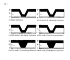
- FIG. 2 shows cross-section photographs of via-holes after electrolytic copper plating using electrolytic copper plating solutions with different MPS concentrations.
- the solution contained no MPS (0 ⁇ g/L)
- via-holes filled completely.
- solutions contained MPS at a concentration of 10 to 1000 ⁇ g/L via-filling was reduced as the concentration increased.
- the appearance of plating was glossy at MPS concentrations up to 100 ⁇ g/L, but became semi-glossy at concentrations of 500 ⁇ g/L and 1000 ⁇ g/L.
- the appearance was glossier at 500 ⁇ g/L than at 1000 ⁇ g/L.
- said electrolytic copper plating solution containing MPS was subjected to dummy electrolysis using an insoluble anode or a soluble anode.
- a phosphated copper anode was used as the soluble anode, and a Pt/Ti mesh was used as the insoluble anode.
- Conditions of dummy electrolysis were the same as the conditions for electrolytic copper plating described above except for the type of anode used and the amount of electrolysis.
- electrolytic copper plating was performed using an electrolytic copper plating solution not containing MPS immediately after setting up the bath, and electrolytic copper plating was performed using the electrolytic copper plating solution containing 1000 ⁇ g/L MPS described above without subjecting to dummy electrolysis. Moreover, all electrolytic copper plating was performed by a soluble anode.
- FIG. 3 shows cross-section photographs of via-holes after electrolytic copper plating under various conditions.
- an electrolytic copper plating solution containing no MPS was used immediately after setting up the bath (No. 1), via-holes were filled without subjecting to dummy electrolysis and the appearance of plating was glossy.
- an electrolytic copper plating solution containing 1000 ⁇ g/L MPS No. 2
- via-filling was incomplete and the appearance of plating was semi-glossy.
- An electrolytic copper plating solution was prepared by dissolving the following chemicals in distilled water: 200 g/L copper sulfate pentahydrate, 100 g/L sulfuric acid, 50 mg/L chloride, 1.5 mg/L bis(3-sulfopropyl)disulfide disodium (SPS), 1500 mg/L cationic surface active agent, and 375 mg/L nonionic surface active agent.
- SPS bis(3-sulfopropyl)disulfide disodium
- direct current was used.
- the electrolytic copper plating solution was subjected to degradation treatment using an electrolytic copper plating apparatus comprised of one main bath and one dummy electrolysis bath.
- degradation treatment refers to performing electrolytic copper plating in the main bath and dummy electrolysis in the dummy electrolysis bath while circulating electrolytic copper plating solution between the main bath and the dummy electrolysis bath in a multi-bath electrolytic copper plating apparatus, and was performed by operating a standard multi-bath electrolytic copper plating apparatus normally.
- the main bath had a bath volume of 4 L and the dummy electrolysis bath had a bath volume of 0.5 L, for a total of 4.5 L electrolytic copper plating solution used.
- the circulation speed of electrolytic copper plating solution between the main bath and the dummy electrolysis bath was 0.7 to 0.9 L/min. Air agitation was performed in both baths. Electrolytic copper plating was performed using a phosphated copper anode as the anode at 23° C plating bath temperature, 2 A/dm 2 (6 A) current density, and an anode area of 1.33 dm 2 per liter of solution. Dummy electrolysis was performed using IrO 2 as the anode at 23° C plating bath temperature, 2 A/dm 2 (0.3 A) current density, and 0.07 dm 2 /L anode area.
- Electrolytic copper plating and dummy electrolysis were stopped at the point when the amount of electrolysis during electrolytic copper plating was 0, 30, 50, or 100 Ahr/L. Moreover, as a control group, said degradation treatment was performed without subjecting to dummy electrolysis in the dummy electrolysis bath.
- electrolytic copper plating was performed on a new evaluation substrate using electrolytic copper plating solution after the degradation treatment described above.
- the evaluation substrate was the same as used in Example 1. Electrolytic copper plating was performed for an electrolysis amount of 50 Ahr/L under the same degradation treatment conditions as given above except for not subjecting to dummy electrolysis in the dummy electrolysis bath. After completing electrolytic copper plating, the evaluation substrate was evaluated for via-filling and plating appearance.
- Figure 4 shows cross-section photographs of via-holes after plating. It was found that when the amount of electrolysis during degradation treatment was 50 Ahr/L or greater and dummy electrolysis was not performed, via-filling was reduced. By contrast, no reduction in filling was found, regardless of the amount of electrolysis, when dummy electrolysis was applied together with electrolytic copper plating during degradation treatment.
- this invention can maintain and restore via-filling ability, fineness of deposited copper films, and plating appearance when these properties of the electrolytic copper plating solution have become degraded.
- this invention can reduce the concentration of compounds having the structure "- X - S - Y -," which is a degradation product of the above-mentioned sulfated compounds, and can maintain and restore via-filling ability, copper film fineness, and plating appearance.
- this invention has the advantages that it does not require a separate treatment to restore the electrolytic copper plating bath, and can save time and effort.
- the electrolytic copper plating method of this invention can decrease the surface area of insoluble anodes used compared to using insoluble anodes for electrolytic copper plating itself. As a result, this invention can decrease the amount of expensive insoluble anodes used, and can reduce overall system costs. Because soluble anodes can be used for electrolytic copper plating, this invention can also reduce the amount of copper salts replenished during plating, and can prevent impurities contained in copper salts being added by this replenishing.
Landscapes
- Chemical & Material Sciences (AREA)
- Engineering & Computer Science (AREA)
- Chemical Kinetics & Catalysis (AREA)
- Electrochemistry (AREA)
- Materials Engineering (AREA)
- Metallurgy (AREA)
- Organic Chemistry (AREA)
- Electroplating And Plating Baths Therefor (AREA)
- Electroplating Methods And Accessories (AREA)
Applications Claiming Priority (2)
| Application Number | Priority Date | Filing Date | Title |
|---|---|---|---|
| JP2001172312 | 2001-06-07 | ||
| JP2001172312 | 2001-06-07 |
Publications (2)
| Publication Number | Publication Date |
|---|---|
| EP1264918A1 true EP1264918A1 (fr) | 2002-12-11 |
| EP1264918B1 EP1264918B1 (fr) | 2011-11-23 |
Family
ID=19013952
Family Applications (1)
| Application Number | Title | Priority Date | Filing Date |
|---|---|---|---|
| EP02253891A Expired - Lifetime EP1264918B1 (fr) | 2001-06-07 | 2002-06-05 | Méthode de placage électrolytique de cuivre |
Country Status (5)
| Country | Link |
|---|---|
| US (1) | US6835294B2 (fr) |
| EP (1) | EP1264918B1 (fr) |
| KR (1) | KR100877923B1 (fr) |
| CN (1) | CN1244720C (fr) |
| TW (1) | TWI268966B (fr) |
Cited By (9)
| Publication number | Priority date | Publication date | Assignee | Title |
|---|---|---|---|---|
| WO2004009876A1 (fr) * | 2002-07-23 | 2004-01-29 | Nikko Materials Co., Ltd. | Solution d'electrolyte de cuivre comprenant un compose amine ayant un squelette specifique et un compose organo-sulfure, et feuille de cuivre electrolytique prepare en utilisant cette solution |
| WO2004035874A1 (fr) * | 2002-10-21 | 2004-04-29 | Nikko Materials Co., Ltd. | Solution electrolytique de cuivre contenant comme additifs un compose sulfure organique et un compose d'amide quaternaire d'un squelette specifique et feuille de cuivre electrolytique produite a l'aide de cette solution |
| DE10325101A1 (de) * | 2003-06-03 | 2004-12-30 | Atotech Deutschland Gmbh | Verfahren zum Auffüllen von µ-Blind-Vias (µ-BVs) |
| DE102004045451A1 (de) * | 2004-09-20 | 2006-03-30 | Atotech Deutschland Gmbh | Galvanisches Verfahren zum Füllen von Durchgangslöchern mit Metallen, insbesondere von Leiterplatten mit Kupfer |
| DE102005014748A1 (de) * | 2005-03-31 | 2006-10-05 | Advanced Micro Devices, Inc., Sunnyvale | Technik zum elektrochemischen Abscheiden einer Legierung mit chemischer Ordnung |
| US8784634B2 (en) | 2006-03-30 | 2014-07-22 | Atotech Deutschland Gmbh | Electrolytic method for filling holes and cavities with metals |
| EP2821530A1 (fr) * | 2013-07-04 | 2015-01-07 | ATOTECH Deutschland GmbH | Dispositif et procédé permettant de conditionner un électrolyte galvanique et activation d'électrodes avant le début d'un processus de dépôt de métal galvanique |
| CN109115860A (zh) * | 2017-06-22 | 2019-01-01 | 台湾积体电路制造股份有限公司 | 电镀工艺的检测方法 |
| WO2021032775A1 (fr) | 2019-08-19 | 2021-02-25 | Atotech Deutschland Gmbh | Fabrication de séquences pour cartes de circuit imprimé d'interconnexion haute densité et carte de circuit imprimé d'interconnexion haute densité |
Families Citing this family (37)
| Publication number | Priority date | Publication date | Assignee | Title |
|---|---|---|---|---|
| US20050109627A1 (en) * | 2003-10-10 | 2005-05-26 | Applied Materials, Inc. | Methods and chemistry for providing initial conformal electrochemical deposition of copper in sub-micron features |
| US20040050706A1 (en) * | 2000-10-10 | 2004-03-18 | Masaru Seita | Copper electroplating method using insoluble anode |
| KR100845189B1 (ko) * | 2000-12-20 | 2008-07-10 | 롬 앤드 하스 일렉트로닉 머트어리얼즈, 엘.엘.씨 | 전해적 구리 도금액 및 이의 제어법 |
| JP2002192648A (ja) * | 2000-12-27 | 2002-07-10 | Learonal Japan Inc | 接合強度が向上された複合材料およびその形成方法 |
| EP1310582A1 (fr) * | 2001-11-07 | 2003-05-14 | Shipley Company LLC | Procédé de placage électrolytique de cuivre |
| JP2003213489A (ja) * | 2002-01-15 | 2003-07-30 | Learonal Japan Inc | ビアフィリング方法 |
| US20030187920A1 (en) * | 2002-04-01 | 2003-10-02 | Tejaswi Redkar | Communication management system |
| EP1475463B2 (fr) * | 2002-12-20 | 2017-03-01 | Shipley Company, L.L.C. | Méthode pour placage électrolytique utilisant du courant pulsé inversé |
| US20040118691A1 (en) * | 2002-12-23 | 2004-06-24 | Shipley Company, L.L.C. | Electroplating method |
| US20050072683A1 (en) * | 2003-04-03 | 2005-04-07 | Ebara Corporation | Copper plating bath and plating method |
| WO2004107422A2 (fr) * | 2003-05-27 | 2004-12-09 | Ebara Corporation | Appareil et procede d'electrodeposition |
| TWI336220B (en) * | 2003-06-20 | 2011-01-11 | Japan Circuit Ind Co Ltd | A method of forming a high density printed wiring board for mounting a semiconductor |
| US20050157475A1 (en) * | 2004-01-15 | 2005-07-21 | Endicott Interconnect Technologies, Inc. | Method of making printed circuit board with electroplated conductive through holes and board resulting therefrom |
| US20070178697A1 (en) * | 2006-02-02 | 2007-08-02 | Enthone Inc. | Copper electrodeposition in microelectronics |
| US8914493B2 (en) * | 2008-03-10 | 2014-12-16 | Oracle International Corporation | Presence-based event driven architecture |
| JP4957906B2 (ja) * | 2007-07-27 | 2012-06-20 | 上村工業株式会社 | 連続電気銅めっき方法 |
| JP5110269B2 (ja) * | 2007-08-09 | 2012-12-26 | 上村工業株式会社 | 電気銅めっき方法 |
| US8303792B1 (en) * | 2007-08-29 | 2012-11-06 | Magnecomp Corporation | High strength electrodeposited suspension conductors |
| US7905994B2 (en) | 2007-10-03 | 2011-03-15 | Moses Lake Industries, Inc. | Substrate holder and electroplating system |
| ITTO20070704A1 (it) * | 2007-10-05 | 2009-04-06 | Create New Technology S R L | Sistema e metodo di placcatura di leghe metalliche mediante tecnologia galvanica |
| US9512012B2 (en) * | 2007-12-08 | 2016-12-06 | Comsats Institute Of Information Technology | Sonoelectrolysis for metal removal |
| US8262894B2 (en) * | 2009-04-30 | 2012-09-11 | Moses Lake Industries, Inc. | High speed copper plating bath |
| JP5471276B2 (ja) * | 2009-10-15 | 2014-04-16 | 上村工業株式会社 | 電気銅めっき浴及び電気銅めっき方法 |
| JP2011127172A (ja) * | 2009-12-17 | 2011-06-30 | Nitto Denko Corp | めっき装置および配線回路基板の製造方法 |
| JP5376168B2 (ja) * | 2010-03-30 | 2013-12-25 | 三菱マテリアル株式会社 | 電気銅めっき用高純度銅アノード、その製造方法および電気銅めっき方法 |
| KR20130108978A (ko) * | 2010-06-11 | 2013-10-07 | 알쉬메 | 구리 도금 조성물 및 이 조성물을 사용한 반도체 기판에서 공동을 충진하기 위한 공정 |
| KR101255548B1 (ko) * | 2011-02-24 | 2013-04-17 | 한양대학교 에리카산학협력단 | 나노쌍정 구조가 형성된 구리재료의 형성방법 |
| JP5851233B2 (ja) | 2011-12-22 | 2016-02-03 | ローム・アンド・ハース電子材料株式会社 | 電解銅めっき液及び電解銅めっき方法 |
| WO2014030779A1 (fr) * | 2012-08-22 | 2014-02-27 | 한양대학교 에리카산학협력단 | Procédé de formation de matière de cuivre formée de façon à avoir une structure nano-bicristalline, et matière de cuivre ainsi obtenue |
| US20140262794A1 (en) * | 2013-03-15 | 2014-09-18 | Applied Materials, Inc. | Electrochemical deposition processes for semiconductor wafers |
| CN104470260B (zh) * | 2013-09-13 | 2018-03-06 | 珠海方正科技高密电子有限公司 | 盲孔电镀填孔方法和电路板 |
| JP6641717B2 (ja) * | 2015-04-08 | 2020-02-05 | 日立化成株式会社 | 多層配線基板の製造方法 |
| US20180298515A1 (en) * | 2015-04-27 | 2018-10-18 | Jcu Corporation | Method for managing copper sulfate plating solution |
| JP6653799B2 (ja) * | 2017-07-31 | 2020-02-26 | メルテックス株式会社 | 電解銅めっき用陽極、及びそれを用いた電解銅めっき装置 |
| DE102018133532A1 (de) * | 2018-12-21 | 2020-06-25 | Maschinenfabrik Kaspar Walter Gmbh & Co Kg | Elektrolyt und Verfahren zur Herstellung von Chromschichten |
| CN109920798B (zh) * | 2019-02-01 | 2021-04-09 | 云谷(固安)科技有限公司 | 阵列基板及其制作方法和显示面板 |
| US11713720B2 (en) | 2019-08-09 | 2023-08-01 | Hamilton Sundstrand Corporation | Turbomachine dual spool transmission systems |
Citations (5)
| Publication number | Priority date | Publication date | Assignee | Title |
|---|---|---|---|---|
| GB2133040A (en) * | 1983-01-03 | 1984-07-18 | Omi Int Corp | Copper plating bath process and anode therefore |
| US4933051A (en) * | 1989-07-24 | 1990-06-12 | Omi International Corporation | Cyanide-free copper plating process |
| JPH04284691A (ja) * | 1991-03-13 | 1992-10-09 | Arumetsukusu:Kk | プリント配線板の電気めっき方法 |
| DE19539865A1 (de) * | 1995-10-26 | 1997-04-30 | Lea Ronal Gmbh | Durchlauf-Galvanikanlage |
| JP2000068651A (ja) * | 1998-08-25 | 2000-03-03 | Nippon Riironaaru Kk | 充填されたブラインドビアホールを有するビルドアッププリント配線板の製造方法 |
Family Cites Families (8)
| Publication number | Priority date | Publication date | Assignee | Title |
|---|---|---|---|---|
| US4376685A (en) * | 1981-06-24 | 1983-03-15 | M&T Chemicals Inc. | Acid copper electroplating baths containing brightening and leveling additives |
| JPH05339800A (ja) * | 1992-06-09 | 1993-12-21 | Nec Corp | 可溶性アノードと不溶性アノードを持つ噴流めっき装置 |
| JPH07336017A (ja) | 1994-06-08 | 1995-12-22 | Hitachi Ltd | 電流反転電解法による薄膜回路製造方法ならびにそれを用いた薄膜回路基板、薄膜多層回路基板および電子回路装置 |
| JP2000087300A (ja) * | 1998-09-08 | 2000-03-28 | Ebara Corp | 基板メッキ装置 |
| JP3293598B2 (ja) * | 1999-07-23 | 2002-06-17 | 日本電気株式会社 | めっき装置とその置換析出防止方法 |
| KR100845189B1 (ko) * | 2000-12-20 | 2008-07-10 | 롬 앤드 하스 일렉트로닉 머트어리얼즈, 엘.엘.씨 | 전해적 구리 도금액 및 이의 제어법 |
| EP1310582A1 (fr) * | 2001-11-07 | 2003-05-14 | Shipley Company LLC | Procédé de placage électrolytique de cuivre |
| JP3976564B2 (ja) * | 2001-12-20 | 2007-09-19 | 日本リーロナール有限会社 | ビアフィリング方法 |
-
2002
- 2002-06-05 TW TW091112064A patent/TWI268966B/zh not_active IP Right Cessation
- 2002-06-05 KR KR1020020031561A patent/KR100877923B1/ko not_active Expired - Lifetime
- 2002-06-05 EP EP02253891A patent/EP1264918B1/fr not_active Expired - Lifetime
- 2002-06-07 CN CNB021286256A patent/CN1244720C/zh not_active Expired - Lifetime
- 2002-06-07 US US10/165,437 patent/US6835294B2/en not_active Expired - Lifetime
Patent Citations (5)
| Publication number | Priority date | Publication date | Assignee | Title |
|---|---|---|---|---|
| GB2133040A (en) * | 1983-01-03 | 1984-07-18 | Omi Int Corp | Copper plating bath process and anode therefore |
| US4933051A (en) * | 1989-07-24 | 1990-06-12 | Omi International Corporation | Cyanide-free copper plating process |
| JPH04284691A (ja) * | 1991-03-13 | 1992-10-09 | Arumetsukusu:Kk | プリント配線板の電気めっき方法 |
| DE19539865A1 (de) * | 1995-10-26 | 1997-04-30 | Lea Ronal Gmbh | Durchlauf-Galvanikanlage |
| JP2000068651A (ja) * | 1998-08-25 | 2000-03-03 | Nippon Riironaaru Kk | 充填されたブラインドビアホールを有するビルドアッププリント配線板の製造方法 |
Non-Patent Citations (2)
| Title |
|---|
| PATENT ABSTRACTS OF JAPAN vol. 017, no. 091 (E - 1324) 23 February 1993 (1993-02-23) * |
| PATENT ABSTRACTS OF JAPAN vol. 2000, no. 06 22 September 2000 (2000-09-22) * |
Cited By (20)
| Publication number | Priority date | Publication date | Assignee | Title |
|---|---|---|---|---|
| US7005055B2 (en) | 2002-07-23 | 2006-02-28 | Nikko Materials Co., Ltd. | Copper electrolytic solution containing amine compound having specific skeleton and organosulfur compound as additives, and electrolytic copper foil produced using the same |
| WO2004009876A1 (fr) * | 2002-07-23 | 2004-01-29 | Nikko Materials Co., Ltd. | Solution d'electrolyte de cuivre comprenant un compose amine ayant un squelette specifique et un compose organo-sulfure, et feuille de cuivre electrolytique prepare en utilisant cette solution |
| WO2004035874A1 (fr) * | 2002-10-21 | 2004-04-29 | Nikko Materials Co., Ltd. | Solution electrolytique de cuivre contenant comme additifs un compose sulfure organique et un compose d'amide quaternaire d'un squelette specifique et feuille de cuivre electrolytique produite a l'aide de cette solution |
| US7144491B2 (en) | 2002-10-21 | 2006-12-05 | Nikko Materials Co., Ltd. | Copper electrolytic solution containing organic sulfur compound and quaternary amine compound of specified skeleton as additives and electrolytic copper foil produced therewith |
| US7771835B2 (en) | 2002-10-21 | 2010-08-10 | Nippon Mining & Metals Co., Ltd. | Copper electrolytic solution containing quaternary amine compound with specific skeleton and oragno-sulfur compound as additives, and electrolytic copper foil manufactured using the same |
| DE10325101A1 (de) * | 2003-06-03 | 2004-12-30 | Atotech Deutschland Gmbh | Verfahren zum Auffüllen von µ-Blind-Vias (µ-BVs) |
| US9445510B2 (en) | 2004-09-20 | 2016-09-13 | Atotech Deutschland Gmbh | Galvanic process for filling through-holes with metals, in particular of printed circuit boards with copper |
| DE102004045451A1 (de) * | 2004-09-20 | 2006-03-30 | Atotech Deutschland Gmbh | Galvanisches Verfahren zum Füllen von Durchgangslöchern mit Metallen, insbesondere von Leiterplatten mit Kupfer |
| US9526183B2 (en) | 2004-09-20 | 2016-12-20 | Atotech Deutschland Gmbh | Galvanic process for filling through-holes with metals, in particular of printed circuit boards with copper |
| DE102004045451B4 (de) * | 2004-09-20 | 2007-05-03 | Atotech Deutschland Gmbh | Galvanisches Verfahren zum Füllen von Durchgangslöchern mit Metallen, insbesondere von Leiterplatten mit Kupfer |
| DE102005014748A1 (de) * | 2005-03-31 | 2006-10-05 | Advanced Micro Devices, Inc., Sunnyvale | Technik zum elektrochemischen Abscheiden einer Legierung mit chemischer Ordnung |
| US7985329B2 (en) | 2005-03-31 | 2011-07-26 | Advanced Micro Devices, Inc. | Technique for electrochemically depositing an alloy having a chemical order |
| DE102005014748B4 (de) * | 2005-03-31 | 2007-02-08 | Advanced Micro Devices, Inc., Sunnyvale | Technik zum elektrochemischen Abscheiden einer Legierung mit chemischer Ordnung |
| US8784634B2 (en) | 2006-03-30 | 2014-07-22 | Atotech Deutschland Gmbh | Electrolytic method for filling holes and cavities with metals |
| EP2821530A1 (fr) * | 2013-07-04 | 2015-01-07 | ATOTECH Deutschland GmbH | Dispositif et procédé permettant de conditionner un électrolyte galvanique et activation d'électrodes avant le début d'un processus de dépôt de métal galvanique |
| WO2015000817A1 (fr) * | 2013-07-04 | 2015-01-08 | Atotech Deutschland Gmbh | Procédé de conditionnement d'un électrolyte galvanique et d'activation d'électrodes avant le démarrage d'un processus de déposition de métal galvanique |
| CN109115860A (zh) * | 2017-06-22 | 2019-01-01 | 台湾积体电路制造股份有限公司 | 电镀工艺的检测方法 |
| CN109115860B (zh) * | 2017-06-22 | 2021-01-08 | 台湾积体电路制造股份有限公司 | 电镀工艺的检测方法 |
| WO2021032775A1 (fr) | 2019-08-19 | 2021-02-25 | Atotech Deutschland Gmbh | Fabrication de séquences pour cartes de circuit imprimé d'interconnexion haute densité et carte de circuit imprimé d'interconnexion haute densité |
| US12063751B2 (en) | 2019-08-19 | 2024-08-13 | Atotech Deutschland GmbH & Co. KG | Manufacturing sequences for high density interconnect printed circuit boards and a high density interconnect printed circuit board |
Also Published As
| Publication number | Publication date |
|---|---|
| KR100877923B1 (ko) | 2009-01-12 |
| US6835294B2 (en) | 2004-12-28 |
| CN1244720C (zh) | 2006-03-08 |
| CN1392294A (zh) | 2003-01-22 |
| US20030015433A1 (en) | 2003-01-23 |
| TWI268966B (en) | 2006-12-21 |
| KR20020093584A (ko) | 2002-12-16 |
| EP1264918B1 (fr) | 2011-11-23 |
Similar Documents
| Publication | Publication Date | Title |
|---|---|---|
| US6835294B2 (en) | Electrolytic copper plating method | |
| US6881319B2 (en) | Electrolytic copper plating solution and method for controlling the same | |
| EP1330146A2 (fr) | Procédé de remplissage de trous de contact | |
| JP4510369B2 (ja) | 電解銅めっき方法 | |
| US20040089557A1 (en) | Process for electrolytic copper plating | |
| US6761814B2 (en) | Via filling method | |
| US3769179A (en) | Copper plating process for printed circuits | |
| JP4481541B2 (ja) | 電解銅めっき液および電解銅めっき液の管理方法 | |
| KR102835665B1 (ko) | 공극을 줄이기 위해 관통 구멍을 충전하는 방법 | |
| US20040050706A1 (en) | Copper electroplating method using insoluble anode | |
| EP2716795B1 (fr) | Liquide et procédé de cuivrage électrolytique | |
| JP3853671B2 (ja) | 電解銅めっき方法 | |
| US20040118691A1 (en) | Electroplating method | |
| EP2669406B1 (fr) | Solution et procédé de cuivrage électrolytique | |
| EP1323850A1 (fr) | Méthode d'électroplacage de circuits imprimés avec une densité de courant pulsée | |
| EP2610370B1 (fr) | Solution de dépôt électrolytique de cuivre et procédé d'électrodéposition de cuivre |
Legal Events
| Date | Code | Title | Description |
|---|---|---|---|
| PUAI | Public reference made under article 153(3) epc to a published international application that has entered the european phase |
Free format text: ORIGINAL CODE: 0009012 |
|
| 17P | Request for examination filed |
Effective date: 20020605 |
|
| AK | Designated contracting states |
Kind code of ref document: A1 Designated state(s): AT BE CH CY DE DK ES FI FR GB GR IE IT LI LU MC NL PT SE TR |
|
| AX | Request for extension of the european patent |
Free format text: AL;LT;LV;MK;RO;SI |
|
| AKX | Designation fees paid |
Designated state(s): DE FR GB |
|
| 17Q | First examination report despatched |
Effective date: 20031110 |
|
| GRAP | Despatch of communication of intention to grant a patent |
Free format text: ORIGINAL CODE: EPIDOSNIGR1 |
|
| RIN1 | Information on inventor provided before grant (corrected) |
Inventor name: HAYASHI, SHINJIRO C/O DORMITORY OF MELTEX Inventor name: KUSAKA, MASARU Inventor name: TSUCHIDA, HIDEKI |
|
| GRAS | Grant fee paid |
Free format text: ORIGINAL CODE: EPIDOSNIGR3 |
|
| GRAA | (expected) grant |
Free format text: ORIGINAL CODE: 0009210 |
|
| AK | Designated contracting states |
Kind code of ref document: B1 Designated state(s): DE FR GB |
|
| REG | Reference to a national code |
Ref country code: GB Ref legal event code: FG4D |
|
| REG | Reference to a national code |
Ref country code: DE Ref legal event code: R096 Ref document number: 60241599 Country of ref document: DE Effective date: 20120202 |
|
| RAP2 | Party data changed (patent owner data changed or rights of a patent transferred) |
Owner name: ROHM AND HAAS ELECTRONIC MATERIALS LLC |
|
| PLBE | No opposition filed within time limit |
Free format text: ORIGINAL CODE: 0009261 |
|
| STAA | Information on the status of an ep patent application or granted ep patent |
Free format text: STATUS: NO OPPOSITION FILED WITHIN TIME LIMIT |
|
| 26N | No opposition filed |
Effective date: 20120824 |
|
| REG | Reference to a national code |
Ref country code: DE Ref legal event code: R097 Ref document number: 60241599 Country of ref document: DE Effective date: 20120824 |
|
| REG | Reference to a national code |
Ref country code: FR Ref legal event code: PLFP Year of fee payment: 15 |
|
| PGFP | Annual fee paid to national office [announced via postgrant information from national office to epo] |
Ref country code: GB Payment date: 20160601 Year of fee payment: 15 |
|
| REG | Reference to a national code |
Ref country code: FR Ref legal event code: PLFP Year of fee payment: 16 |
|
| GBPC | Gb: european patent ceased through non-payment of renewal fee |
Effective date: 20170605 |
|
| PG25 | Lapsed in a contracting state [announced via postgrant information from national office to epo] |
Ref country code: GB Free format text: LAPSE BECAUSE OF NON-PAYMENT OF DUE FEES Effective date: 20170605 |
|
| REG | Reference to a national code |
Ref country code: FR Ref legal event code: PLFP Year of fee payment: 17 |
|
| PGFP | Annual fee paid to national office [announced via postgrant information from national office to epo] |
Ref country code: FR Payment date: 20190510 Year of fee payment: 18 |
|
| PG25 | Lapsed in a contracting state [announced via postgrant information from national office to epo] |
Ref country code: FR Free format text: LAPSE BECAUSE OF NON-PAYMENT OF DUE FEES Effective date: 20200630 |
|
| PGFP | Annual fee paid to national office [announced via postgrant information from national office to epo] |
Ref country code: DE Payment date: 20210511 Year of fee payment: 20 |
|
| REG | Reference to a national code |
Ref country code: DE Ref legal event code: R071 Ref document number: 60241599 Country of ref document: DE |