EP1265086A2 - Kompensationsanordnung und -verfahren mit in Abschnitte zerlegten Bragg-Gittern - Google Patents
Kompensationsanordnung und -verfahren mit in Abschnitte zerlegten Bragg-Gittern Download PDFInfo
- Publication number
- EP1265086A2 EP1265086A2 EP02253894A EP02253894A EP1265086A2 EP 1265086 A2 EP1265086 A2 EP 1265086A2 EP 02253894 A EP02253894 A EP 02253894A EP 02253894 A EP02253894 A EP 02253894A EP 1265086 A2 EP1265086 A2 EP 1265086A2
- Authority
- EP
- European Patent Office
- Prior art keywords
- waveguide
- dispersion
- refractive index
- grating
- length
- Prior art date
- Legal status (The legal status is an assumption and is not a legal conclusion. Google has not performed a legal analysis and makes no representation as to the accuracy of the status listed.)
- Withdrawn
Links
Images


Classifications
-
- G—PHYSICS
- G02—OPTICS
- G02B—OPTICAL ELEMENTS, SYSTEMS OR APPARATUS
- G02B6/00—Light guides; Structural details of arrangements comprising light guides and other optical elements, e.g. couplings
- G02B6/24—Coupling light guides
- G02B6/26—Optical coupling means
- G02B6/28—Optical coupling means having data bus means, i.e. plural waveguides interconnected and providing an inherently bidirectional system by mixing and splitting signals
- G02B6/293—Optical coupling means having data bus means, i.e. plural waveguides interconnected and providing an inherently bidirectional system by mixing and splitting signals with wavelength selective means
- G02B6/29379—Optical coupling means having data bus means, i.e. plural waveguides interconnected and providing an inherently bidirectional system by mixing and splitting signals with wavelength selective means characterised by the function or use of the complete device
- G02B6/29392—Controlling dispersion
- G02B6/29394—Compensating wavelength dispersion
-
- G—PHYSICS
- G02—OPTICS
- G02B—OPTICAL ELEMENTS, SYSTEMS OR APPARATUS
- G02B6/00—Light guides; Structural details of arrangements comprising light guides and other optical elements, e.g. couplings
- G02B6/10—Light guides; Structural details of arrangements comprising light guides and other optical elements, e.g. couplings of the optical waveguide type
- G02B6/12—Light guides; Structural details of arrangements comprising light guides and other optical elements, e.g. couplings of the optical waveguide type of the integrated circuit kind
- G02B6/12007—Light guides; Structural details of arrangements comprising light guides and other optical elements, e.g. couplings of the optical waveguide type of the integrated circuit kind forming wavelength selective elements, e.g. multiplexer, demultiplexer
-
- G—PHYSICS
- G02—OPTICS
- G02B—OPTICAL ELEMENTS, SYSTEMS OR APPARATUS
- G02B6/00—Light guides; Structural details of arrangements comprising light guides and other optical elements, e.g. couplings
- G02B6/10—Light guides; Structural details of arrangements comprising light guides and other optical elements, e.g. couplings of the optical waveguide type
- G02B6/12—Light guides; Structural details of arrangements comprising light guides and other optical elements, e.g. couplings of the optical waveguide type of the integrated circuit kind
- G02B2006/12083—Constructional arrangements
- G02B2006/12107—Grating
-
- G—PHYSICS
- G02—OPTICS
- G02B—OPTICAL ELEMENTS, SYSTEMS OR APPARATUS
- G02B6/00—Light guides; Structural details of arrangements comprising light guides and other optical elements, e.g. couplings
- G02B6/02—Optical fibres with cladding with or without a coating
- G02B6/02057—Optical fibres with cladding with or without a coating comprising gratings
- G02B6/02076—Refractive index modulation gratings, e.g. Bragg gratings
- G02B6/0208—Refractive index modulation gratings, e.g. Bragg gratings characterised by their structure, wavelength response
- G02B6/02085—Refractive index modulation gratings, e.g. Bragg gratings characterised by their structure, wavelength response characterised by the grating profile, e.g. chirped, apodised, tilted, helical
-
- G—PHYSICS
- G02—OPTICS
- G02B—OPTICAL ELEMENTS, SYSTEMS OR APPARATUS
- G02B6/00—Light guides; Structural details of arrangements comprising light guides and other optical elements, e.g. couplings
- G02B6/02—Optical fibres with cladding with or without a coating
- G02B6/02057—Optical fibres with cladding with or without a coating comprising gratings
- G02B6/02076—Refractive index modulation gratings, e.g. Bragg gratings
- G02B6/02195—Refractive index modulation gratings, e.g. Bragg gratings characterised by means for tuning the grating
- G02B6/02204—Refractive index modulation gratings, e.g. Bragg gratings characterised by means for tuning the grating using thermal effects, e.g. heating or cooling of a temperature sensitive mounting body
-
- G—PHYSICS
- G02—OPTICS
- G02B—OPTICAL ELEMENTS, SYSTEMS OR APPARATUS
- G02B6/00—Light guides; Structural details of arrangements comprising light guides and other optical elements, e.g. couplings
- G02B6/24—Coupling light guides
- G02B6/26—Optical coupling means
- G02B6/28—Optical coupling means having data bus means, i.e. plural waveguides interconnected and providing an inherently bidirectional system by mixing and splitting signals
- G02B6/293—Optical coupling means having data bus means, i.e. plural waveguides interconnected and providing an inherently bidirectional system by mixing and splitting signals with wavelength selective means
- G02B6/29304—Optical coupling means having data bus means, i.e. plural waveguides interconnected and providing an inherently bidirectional system by mixing and splitting signals with wavelength selective means operating by diffraction, e.g. grating
- G02B6/29316—Light guides comprising a diffractive element, e.g. grating in or on the light guide such that diffracted light is confined in the light guide
- G02B6/29317—Light guides of the optical fibre type
- G02B6/29322—Diffractive elements of the tunable type
Definitions
- This invention relates to the compensation of chromatic dispersion, hereinafter referred to as dispersion, in optical transmission systems.
- this invention relates to the compensation of dispersion in Wavelength Division Multiplexed (WDM) optical communications systems.
- WDM Wavelength Division Multiplexed
- chromatic dispersion is the dependence of wave velocity on wavelength as a wave travels through a medium.
- chromatic dispersion is used to refer to the dependence of group delay, ⁇ , on wavelength, .
- Linear dispersion is typically measured in picoseconds per nanometre (ps/nm).
- the linear dispersion exhibited by the medium is proportional to its length and so, for such a medium, it is convenient to define its linear dispersion per unit length, also known as its linear dispersion power. This is typically measured in picoseconds per nanometre per kilometre (ps/nm/km).
- dispersion In a digital transmission system the presence of dispersion leads to pulse broadening, and hence to a curtailment of system reach before some form of pulse regeneration becomes necessary.
- the problem presented by dispersion increases rapidly with increasing bit rate. This is because, on the one hand, increasing the bit rate produces increased spectral broadening of the pulses, and hence increased dispersion mediated pulse broadening; while on the other hand, increasing the bit rate also produces a reduction in the time interval between consecutive bits.
- it is not practical to minimise the problems of dispersion by choosing to employ a transmission medium exhibiting near-zero first order dispersive power because low first order dispersive power is associated with aggravated non-linear (e.g. four-wave mixing) distortion.
- a known solution to this problem is to employ "managed dispersion" in which near-zero aggregate linear dispersion over a particular transmission path is achieved by the use of alternating sections respectively exhibiting positive linear dispersion and negative linear dispersion, for instance by the use of non-dispersion-shifted (NDS) and dispersion compensating (DC) optical fibre waveguide.
- NDS non-dispersion-shifted
- DC dispersion compensating
- dispersion compensation devices based on spectrally distributed reflection of optical signals from waveguides incorporating chirped Bragg gratings (i.e. gratings in which the effective pitch n eff . ⁇ varies along the grating's length, where n eff is the effective refractive index and ⁇ is the physical pitch).
- gratings in which the effective pitch n eff . ⁇ varies along the grating's length, where n eff is the effective refractive index and ⁇ is the physical pitch.
- the chirped Bragg grating exhibits/provides chromatic dispersion because signal components at different wavelengths will be reflected, effectively, at different positions along the grating's length, and so will have been delayed by different amounts of time when they reemerge from the waveguide after reflection.
- adjustable dispersion compensation devices in which the effective pitch of a Bragg reflection grating is adjusted by applying uniform or non-uniform strain (to alter physical pitch) or by applying a thermal gradient (to alter effective refractive index). For a grating with uniform physical pitch, controlling the magnitude of the thermal gradient controls the magnitude of the resulting chirp, and thus there is provided a form of adjustable amplitude linear dispersion compensation device.
- Such a device is for instance described by B J Eggleton et al. in, "Dispersion compensation in 20Gbit/s dynamic nonlinear lightwave systems using electrically tunable chirped fibre grating", Electronics Letters Vol. 35, No. 10, pp 832-3.
- Etalon-based devices have also been used for dispersion compensation purposes, but have insufficient dispersion and slope uniformity within the information bandwidth to be applicable in high spectral density, high bit rate WDM systems.
- Embodiments of the present invention therefore aim to provide dispersion compensation apparatus, and corresponding methods, which overcome, at least partially, one or more of the above-mentioned problems/disadvantages associated with the prior art.
- a further object of embodiments not least for reasons of minimising inventory, for operating in a WDM system, is to provide a Bragg grating dispersion compensator that is capable of providing dispersion compensation for any individual one of the channels of that WDM system.
- dispersion compensation apparatus comprising a waveguide comprising a sampled Bragg grating extending along a length of the waveguide, the sampled Bragg grating exhibiting a comb-link reflectance versus wavelength spectrum comprising a plurality of teeth; and adjustment apparatus arranged to adjust an effective refractive index of the waveguide along at least a portion of said length.
- the positions of the teeth in the spectrum may, for example, be shifted to bring one of the teeth into register with a bandwidth of a signal input to the waveguide, and/or the dispersion exhibited by the grating may be adjusted.
- Sampled Bragg gratings are known.
- the effective refractive index along the waveguide structure is modulated in some way (e.g. in a periodic fashion) to produce the grating "elements".
- the depth of the refractive index modulation is itself modulated in some fashion.
- the sampled gratings comprise a sequence of groups of grating elements, connected by sections of waveguide in which the effective refractive index is substantially unmodulated (i.e. they contain no grating elements).
- the effective refractive index is substantially unmodulated (i.e. they contain no grating elements).
- this is not essential, and a comb-like response may be exhibited by a sampled grating where the modulation depth is modulated in some other fashion (e.g. it just varies sinusoidally along the waveguide's length, never reaching zero).
- the term "sampled Bragg grating” is intended to encompass any Bragg grating arranged to provide a comb-like reflectance characteristic (i.e. repeated pass/reflection bands).
- the sampled grating consists of a sequence of groups of grating elements (i.e. grating samples) spaced apart along the length of the waveguide in which the grating is formed.
- the sampled grating described above will give approximately the same peak reflectance as the original unsampled grating, with the pass-band repeating at a frequency which depends on the sample period.
- the sampled grating exhibits a comb-like reflectance characteristic, with the spacing of the "teeth" of the comb being determined by the optical path length between the samples.
- This optical path length depends on the physical separation of the samples and the effective refractive index of the portions of the waveguide connecting the samples.
- This comb-like characteristic results from the fact that each short grating sample acts as a broad-band reflector. Reflected signal components at a wavelength from adjacent samples will constructively interfere if where k is an integer, n eff is the effective refractive index of the waveguide connecting the samples, and B is the sample period.
- Each "tooth” will have substantially the same shape and width as the single reflectance band provided by the corresponding unsampled grating. Furthermore, when a signal whose bandwidth lies within a particular tooth is reflected by the sampled grating, the signal has imparted to it substantially the same dispersion as would be imparted to a corresponding signal on reflection by the corresponding unsampled grating,
- sampling a grating results in a repetition of its reflectance (including dispersion) characteristics at a plurality of positions in the wavelength spectrum.
- the reflection characteristics corresponding to a particular tooth in the reflection spectrum are determined by the sampled grating as a whole, and the positions of the teeth are determined by the sampling period and refractive index along the grating.
- the dispersion compensation apparatus provides the advantage that, by employing a sampled grating having a comb-link reflectance spectrum, then provided that a signal bandwidth lies within the comb it is only necessary to adjust the refractive index along the waveguide by a small amount in order to bring one of the teeth of the comb into register with the signal bandwidth to reflect it. Thus, tuning may be achieved quickly.
- the same dispersion compensation apparatus can be used to compensate for dispersion in any signal having a bandwidth lying within the comb characteristics, so the same apparatus can be used to compensate for dispersion in all channels of a WDM system.
- a corresponding number of nominally identical designs in accordance with the first aspect of the present invention can be used.
- a further advantage is that, by adjusting the effective refractive index along the grating's length, the dispersion provided to a signal on reflection may be adjusted/controlled.
- the adjustment apparatus is arranged to control the average value of effective refractive index over the length. This may be achieved by making a uniform change to the value of the refractive index all along the length, or by simply altering its values at specific points along that length.
- the adjustment apparatus is also arranged to set a desired distribution of effective refractive index along this length. In this way, the dispersion exhibited by the device to incident optical signals can be controlled and adjusted.
- the grating is pre-chirped, but alternatively a chirp may be introduced by suitable adjustment of the refractive index profile along the length.
- control of effective refractive index along the length of the waveguide is achieved by controlling the temperature profile of a cladding material over, under, or surrounding a waveguide core.
- the refractive index control is achieved by using a waveguide which has a core and a plurality of slots interrupting the core, each slot being filled with a material having a high temperature coefficient of refractive index or a refractive index which is a function of applied electric field.
- a material having a high temperature coefficient of refractive index or a refractive index which is a function of applied electric field By controlling the temperature or electric field applied to the material in each slot a desired average effective refractive index or distribution along the length of the waveguide can be achieved.
- the slots are arranged between each and every pair of adjacent grating samples along the waveguide, such that by adjusting the effective refractive index of the material in the slots, the optical path lengths between the grating samples, and hence the reflectance properties of the grating, can be controlled.
- a further aspect of the present invention provides dispersion compensation apparatus comprising: a waveguide comprising a sampled Bragg grating extending along a length of the waveguide, the sampled Bragg grating exhibiting a comb-like reflectance versus wavelength spectrum comprising a plurality of teeth; and adjustment apparatus for controlling an effective refractive index profile of the waveguide along said length.
- Such apparatus provides the advantage that the positions of the teeth and/or the dispersion exhibited by the device can be adjusted so as to compensate for dispersion in any signal having a bandwidth lying within the comb spectral characteristics.
- a further aspect of the present invention provides a waveguide comprising: a core formed from a first material; a sampled Bragg grating comprising a sequence of grating samples spaced apart along said core; and a plurality of waveguide sections formed from a second material, each section at least partially interrupting the core and being arranged in the optical path between a respective pair of adjacent grating samples, the second material having a higher thermal coefficient of refractive index than the first, whereby the optical path lengths between the samples, and hence the reflectance characteristics of the grating, may be adjusted by controlling the temperature of the sections.
- the second material is a material whose refractive index is dependent on applied electric field.
- a method of compensating for dispersion in an optical signal having a bandwidth comprising the steps of: inputting the signal to a waveguide comprising a chirped sampled Bragg grating extending along a length of the waveguide, the chirped sampled Bragg grating exhibiting a comb-like reflectance versus wavelength spectrum comprising a plurality of teeth; shifting the position of said teeth in the reflectance spectrum by adjusting the effective refractive index of the waveguide along at least a portion of said length, such that one of said teeth spans said bandwidth; and reflecting the optical signal from the chirped sampled Bragg grating.
- the shifting is achieved by adjusting the effective refractive index at a plurality of positions along the length, preferably by the same amount so as to increase or decrease the average effective refractive index along the length.
- each position lies between a respective pair of adjacent samples of the sampled Bragg grating.
- a respective one of said plurality of positions lies between each pair of adjacent samples, such that the step of shifting comprises adjusting the effective refractive index of the waveguide between every pair of adjacent samples.
- the shifting is achieved by altering the temperature or the electric field applied to portions of the waveguide between each pair of adjacent grating samples.
- This effective refractive index "profile” may be achieved by applying a continuous variation in effective refractive index over the length, or by controlling refractive index at a plurality of distinct positions along the length. These separate positions are preferably located between adjacent grating samples.
- the desired distribution of effective refractive index along the length may be achieved by controlling the temperature of or the electric field applied to sections of the waveguide distributed along its length.
- the waveguide comprises a core, and a plurality of slots interrupting the core, each slot being arranged at a respective one of said plurality of positions and being filled with a material having a high temperature coefficient of refractive index, and wherein the step of shifting comprises adjusting the temperature of the material in each slot.
- each slot is positioned between a respective pair of adjacent samples of the sampled Bragg grating.
- a respective slot is positioned between each pair of adjacent samples, such that the step of shifting comprises adjusting the temperature of the material in the slots between every pair of adjacent samples.
- the waveguide comprises a core and a plurality of slots interrupting the core, each slot being arranged at a respective one of said plurality of positions and being filled with a material having a refractive index which is dependent on applied electric field, and wherein the step of shifting comprises adjusting an electric field applied to the material in each slot.
- each slot is positioned between a respective pair of adjacent samples of the sampled Bragg grating.
- a respective slot is positioned between each pair of adjacent samples, such that the step of shifting comprises adjusting the electric field applied to the material in the slots between every pair of adjacent samples.
- said step of shifting comprises adjusting the effective refractive index by a uniform amount along said length.
- the waveguide comprises a core and a cladding
- the step of shifting comprises making a substantially uniform adjustment to the temperature of said cladding along said length.
- said cladding comprises a material having a high temperature coefficient of refractive index.
- the method further comprises the step of altering the dispersion imparted to the optical signal by said reflection by adjusting the effective refractive index of the waveguide along at least a portion of said length to provide a variation in effective refractive index along said length and, optionally, wherein said variation comprises a linear or quadratic component.
- said step of altering the dispersion comprises adjusting the refractive index at each of a plurality of positions distributed along said length.
- each said position lies between a respective pair of adjacent samples of the sampled Bragg grating.
- a respective one of said plurality of positions lies between each pair of adjacent samples, such that the step of altering the dispersion comprises adjusting the effective refractive index of the waveguide between every pair of adjacent samples.
- the waveguide comprises a core, and a plurality of slots interrupting the core, each slot being arranged at a respective one of said plurality of positions and being filled with a material having a high temperature coefficient of refractive index, and wherein the step of altering the dispersion comprises adjusting the temperature of the material in each slot.
- a respective slot is positioned between each pair of adjacent samples, such that the step of altering the dispersion comprises adjusting the temperature of the material in the slops between every pair of adjacent samples.
- the waveguide comprises a core and a plurality of slots interrupting the core, each slot being arranged at a respective one of said plurality of positions and being filled with a material having a refractive index which is dependent on applied electric field, and wherein the step of altering the dispersion comprises adjusting an electric field applied to the material in each slot.
- each slot is positioned between a respective pair of adjacent samples of the sampled Bragg grating.
- a respective slot is positioned between each pair of adjacent samples, such that the step of altering the dispersion comprises adjusting the electric field applied to the material in the slots between every pair of adjacent samples.
- said step of altering the dispersion comprises the step of setting a desired continuous distribution of effective refractive index along said length.
- the waveguide comprises a core and a cladding, and said distribution is set by applying a temperature or electric field distribution to the cladding along said length.
- a method of compensating for dispersion in an optical signal having a bandwidth comprising the steps of: inputting the signal to a waveguide comprising a sampled Bragg grating extending along a length of the waveguide, the sampled Bragg grating exhibiting a comb-like reflectance versus wavelength spectrum comprising a plurality of teeth; chirping the sampled Bragg grating by adjusting the effective refractive index of the waveguide at a plurality of position along said length to set a variation in effective refractive index along said length; shifting the positions of said teeth in the reflectance spectrum by further adjusting the effective refractive index at said plurality of positions, such that one of said teeth spans said bandwidth; and reflecting the optical signal from the chirped, sampled Bragg grating.
- the sampled Bragg grating may initially be unchirped, with all of the chirp for dispersion compensation purposes being provided by the applied effective refractive index variation along the length of the waveguide.
- a method of compensating for dispersion in an optical signal being a bandwidth comprising the steps of: inputting the signal to a waveguide comprising a chirped sampled Bragg grating extending along a length of the waveguide, the chirped sampled Bragg grating exhibiting a comb-like reflectance versus wavelength spectrum comprising a plurality of teeth; controlling the profile of the waveguide's effective refractive index along said length to adjust the position of the teeth in the spectrum to bring one of the teeth into register with the signal bandwidth to reflect the signal, and to adjust the dispersion imported to the signal by said reflection.
- a method of compensating for dispersion in an optical signal comprising the steps of:inputting the signal to a waveguide comprising a sampled Bragg grating extending along a length of the waveguide; reflecting the signal from the sampled Bragg grating; and adjusting the profile of the waveguide's effective refractive index along said length to adjust the dispersion imparted to the signal by said reflection.
- the sampled Bragg grating exhibits a comb-like reflectance versus wavelength spectrum comprising a plurality of teeth
- the step of adjusting comprises adjusting the position of the teeth in the spectrum to bring one of the teeth into register with the bandwidth of the signal.
- adjustable filters, line amplifiers, and receivers for WDM optical communications systems incorporating waveguides with sampled Bragg gratings in which effective refractive index can be controlled over the grating's length.
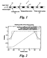
- Figure 1 shows a section of a waveguide 1 embodying the invention, which preferably is single moded at wavelength of operation.
- the effective index of the guide is modulated to form a Bragg grating.
- the modulation may be achieved by a varying the refractive index of the core, the refractive index of the cladding, the core transverse dimensions or the shape of the core cross-section.
- the sampled Bragg grating comprises a sequence of grating sections (samples) 21 spaced out at substantially regular intervals along the waveguide core 11.
- regions of high refractive index material are embedded in either or both of the core or cladding of the waveguide.
- the strength of each of the grating sections 21 is varied by adjusting the refractive index, volume or shape of the deposited material. It may be advantageous to apply a smooth variation in grating pitch along the device.
- the waveguide also contains sections in which the effective index of the guided mode may be varied by some means.
- transverse slots are cut into the waveguide, and filled with a material such as a polymer with a higher temperature coefficient of refractive index than silica, or a liquid crystal or other material whose refractive index may be varied by an applied electric field.
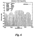
- the wavelength, ,of peak reflectance of a Bragg grating is determined by the pitch 7 of the refractive index modulation, i.e. by where n eff is the effective index of the mode, usually intermediate between the refractive indices of the core and cladding materials for a guided mode.
- the reflectance of the filter is high and uniform in the pass band, and decays rapidly outside the passband. This minimises distortion of the wanted signal, and interference from unwanted signals at other wavelengths.
- Figure 2 shows two apodisation profiles for a 60mm long device.
- grating strength 0.6mm transition from low to high coupling strength
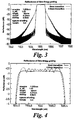
- Figure 4 shows the additional benefits of smooth apodisation, in reducing amplitude ripple within the passband.
- Figure 5 shows the associated improvement in group delay ripple. Dispersion in the centre of the band is approximately 550ps/nm.
- Figures 7 and 8 show a preferred manufacturing route, using silica on silicon planar waveguide techniques for manufacturing a waveguide embodying the present invention. Layers of glass of appropriate refractive index and thermal properties are deposited, and etched in sequence to give the required waveguide structure.
- Silicon nitride has a high refractive index compared with silica, and provides the required index modulation for the grating regions, even when deposited as a relatively thin film. Thin films of silicon nitride can be etched to the required shape with high accuracy.
- Figures 7 and 8 show areas of Si 3 N 4 positioned within the core of a planar waveguide.
- Si 3 N 4 regions located above and/or below the core will also provide the required index modulation, as will regions laterally displaced in the cladding. Such arrangements are used in alternative embodiments.
- Modulation of the core width, thickness, or refractive index are also possible, but may not provide as wide a range of performance as the silicon nitride approach.
- the upper cladding shown in figure 8 may be either a glass or a polymer layer with a refractive index lower than that of the core glass.
- the simplest option is to over-clad a ridge waveguide using a polymeric or similar material with a lower refractive index than the core material, and a high temperature coefficient of refractive index. This will provide the required variation of effective index as the temperature and temperature gradient along the guide are varied.
- a possible side-effect is a variation of the strength of the grating as the cladding index varies.
- An increase in cladding index will decrease the fraction of power within the core, and reduce the overlap between the fibre mode and a grating written in the core.
- Such effects are minimised by operating with a relatively high index difference in the core (0.01 or larger), and/or by extending the index modulation outside the core.
- variable refractive index material is located in slots in the waveguide, i.e. this is preferable to overcladding.
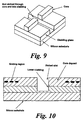
- Figure 9 shows a ridge waveguide with slots etched transversely through the core (and preferably at least part way into the cladding, though this is not essential).
- Figure 10 is a cross-section through such an etched waveguide.
- Electro-optic tuning is a further tuning option, and can provide a fast response.
- Suitable materials are available whose refractive index varies with applied electric field.
- Liquid crystal materials are examples with relatively large refractive index changes for small applied electric fields.
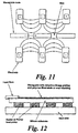
- Figure 11 shows an example of a slotted waveguide and an arrangement of electrodes which gives a substantially axial electric field in the slots, which contain a suitable electro-optic material. This arrangement is employed in a dispersion compensator embodying the invention.
- the applied electric field makes the electro-optic material birefringent.
- the polarisation dependence for an optical signal propagating in the waveguide is small when the electric field is parallel to the direction of propagation.
- An alternative disposition of electrodes is possible with certain classes of optical anisotropy in the electro-optic material.
- Temperature tuning is a further option, used in certain embodiments.
- One option used for temperature tuning is to deposit heating elements on the silica on silicon waveguide, close to the waveguide.
- the temperature gradients required to achieve a useful tuning range are relatively low.
- An alternative method is to heat or cool the waveguide structure using a number of Peltier devices.
- Figure 12 shows one configuration.
- the response time of such a device will be slower than for the case where heaters are located within a few tens of microns of the waveguide core, but with appropriate thermal design, the power consumption could be lower.
- planar waveguide techniques can fabricate substantially identical waveguides on the same wafer.
- An alternative method is to use two identical waveguide Bragg gratings in series.
- the output polarisation state from the first waveguide is rotated through 90 degrees before transmission through the second waveguide Bragg grating.
- Both polarisation states are reflected via the slow axis of one waveguide grating, and via the fast axis of the identical second grating, minimising any differential group delay between the two polarisation states.
- the polarisation rotation may be implemented using waveplates operating on an expanded beam, or by using polarisation maintaining fibre, with a 90 degree twist between the two devices, or by insertion of this film waveplates in narrow slots (typically 10:m or less in width).
- Figure 14 shows an example of this configuration. Because of the additional circulator stage, and Bragg reflection, the insertion loss may be higher than for the method shown in figure 13. However because each polarisation is reflected from both Bragg gratings, the dispersion is twice that achievable from a single reflection, assuming identical waveguide length, chirp rate, and bandwidth.
- An alternative implementation would use expanded beams, polarising beam splitters, and wave plates to rotate the polarisation states, similar to the techniques used in isolators, circulators, and in figure 13.
- One aspect of the present invention is directed to a method of manufacturing sampled dispersion compensation gratings with a periodic passband response.
- the design is implemented in a planar waveguide technology.
- Use of a polymer cladding or polymer-filled waveguide slots enables electrical or thermal tuning of both dispersion and dispersion slope, over a broader range than is practical in a device relying entirely on silica-based glasses in the signal path.
- High bit rate wavelength division multiplexed (WDM) optical communications systems operating at 40Gbit/s and higher rates, require per-channel dispersion compensation. If second order dispersion (dispersion slope) is sufficiently high, then pulse distortion occurs, and compensation for dispersion slope improves performance. Embodiments of the present invention provide such compensation.
- the device is fabricated as a series of short sections.
- an overall spectral width (at -1dB insertion loss) of 30nm is possible with a section length of 0.01mm.
- Narrower reflecting regions will give a broader spectral response, but will require a higher index modulation in the grating. This is possible using the technique described.
- a sample repeat period of 0.26mm gives a free spectral range of 400 GHz. 0.13mm gives an 800GHz FSR.
- Thermal tuning may be provided by manufacturing the upper cladding layer of the waveguide from a polymer, or other material, preferably with a higher temperature coefficient of refraction than silica. Silicone-based polymers are available with suitable refractive index values, but other materials may be used. Alternatively, slots of 0.002 to 0.02mm width may be cut or etched in the waveguide, between the grating sections, and filled with a suitable polymer. This allows the average refractive index of the waveguide to be adjusted, by changing the temperature. The constraints on the absolute refractive index of the material are less stringent than for the over-clad option. Some liquid crystal materials exhibit a refractive index which varies with electric field. These may either be used as cladding materials, or in the filled slot configuration.
- the pass band response of the filter is controlled by the overall length, chirp and apodisation of the sampled grating.
- a length of 60mm is readily fabricated on a silicon wafer without bends. This is ample to provide up to 600ps/nm dispersion over a 0.5nm spectral window.
- the grating chirp, and hence the dispersion is tuned by inducing a temperature gradient along the grating. With typical material and device parameters, 50 degrees difference along the grating is sufficient to change the dispersion from 550ps/nm to 80ps/nm. A smaller temperature range may be adequate for many applications, and will reduce power consumption, and minimise variations in insertion loss.
- Dispersion slope is provided by making the temperature gradient vary with position. 50ps/nm/nm/km dispersion slope is achievable over 1nm bandwidth. Much higher slopes are possible over a narrow window.
- Embodiments provide per-channel dispersion compensation, required for high capacity transport systems, operating at 40 Gbit/s.
- the periodic pass band allows a single compensator unit to be suitable for any one of a range of WDM channels, reducing parts count, inventory and cost. It allows receiver modules to be generic, rather than channel specific. At 80 Gbit/s dispersion slope compensation may be required.
- a comb filter spectral characteristic is provided by a sampled Bragg fibre grating.
- the optical path length extending between each adjacent pair of grating samples is adjustable using a high (thermal or electric field) coefficient material to load the waveguide, or to fill transverse slots milled in the waveguide core.
- a uniform magnitude of adjustment serves to shift the spectral position of the teeth so that one of them can be brought into registry with any chosen WDM channel lying within the spectral band covered by the comb.
- a superimposed linearly graded adjustment along the length of the sampled grating then adjusts the magnitude of the dispersion afforded to that channel.
- different gratings of the same design can be employed for dispersion compensation of different WDM channels. (If designed, a quadratic grating can be further superimposed on the linear grading).
- top hat modulation This is for simplicity of simulation and visualisation, and is not essential. With some fabrication techniques, it will not be possible to achieve a sharp cut-off. This is not necessarily a problem, and may be desirable if a smooth roll-off of the transmission of the outer pass bands is required. Using the described lithographic technique, this is available as a design parameter. In such cases we need not include an exact integer number of grating periods.
- the rate of chirp in preferred embodiments will generally be relatively slow, so the number of grating periods will not change significantly along the grating.
- Sampled Bragg gratings give a periodic pass-band response, so a single device according to the present invention can be used over a wide range of wavelengths.
- Bragg grating chirp rate and effective pitch may be varied by adjusting the temperature or electric field applied to polymer-filled slots in the waveguide.
- Centre wavelength of the pass-band of the grating may be adjusted by varying the mean index of the polymer.
- Dispersion may be adjusted by varying the chirp rate, e.g. by a field or temperature gradient.
- Dispersion slope may be compensated by applying a non-uniform field or temperature gradient.
- the sampled gratings utilised in embodiments of the present invention have one or more of the following preferred features:
- Useful devices can still be fabricated if some of these preferences are not fully met, but aspects of performance, such as insertion loss uniformity between pass-bands, or the useable operating wavelength range, may be compromised.
- the waveguide has a planar waveguide structure.
- the grating elements are formed by depositing silicon nitride in the centre of the waveguide (e.g. in the centre of the core).
- the silicon nitride (Si 3 N 4 ) deposits can be made above and/or the waveguide core.
- slots are etched into the waveguide structure, to be filled by suitable materials such as a polymer.
- the gratings used by embodiments of the present invention may be manufactured in any one of a large number of ways.
- the grating elements may be formed by modulating the core thickness, by modulating the core width, or by modulating the core composition (for example by ion implantation, in-diffused, or deposited dopants).
- the gratings utilised by embodiments of the present invention are apodised, i.e. the coupling strength is apodised, and the chirp at the ends of the grating is varied to minimise delay ripple, among other things.
- the cladding refractive index may be temperature tuned to vary the coupling strength with chirp. Also, dispersion slope may be adjusted by appropriate control of refractive index profile along the length of the grating.
- a waveguide comprising a sampled Bragg grating is that it is a waveguide with a periodic modulation of the refractive index or waveguide geometry.
- the depth of the periodic modulation is itself modulated, so that the waveguide comprises short Bragg grating segments, separated by substantially unmodulated sections.
- means are provided to vary the effective refractive index of the unmodulated segments of the waveguide.
- the unmodulated sections of the waveguide include parts which are constructed from material whose refractive index may be controlled by an applied electric field.
- those parts may be constructed from a material with a high temperature coefficient of refractive index.
- part of the optical cladding to the waveguide comprises a material with lower refractive index than the waveguide core, and which has a high temperature coefficient refractive index.
- part of the optical cladding to the waveguide comprises a material with a lower refractive index and the waveguide core, and whose refractive index may be modified by an applied electric field.
- the centre frequency of the pass-band can be adjusted within the free spectral range by changing the mean index of the tuning slots (i.e. the mean temperature of the device).
- the dispersion compensation device is fabricated from a sequence of grating sections, separated by uniform index regions containing one or more slots in the waveguide. These waveguide slots are filled with material whose refractive index is close to that of the waveguide, but whose precise value can be modified, for example by changing the temperature, or applying an electric field.
- the dispersion is inversely proportional to the chirp rate of that part of the grating where the Bragg condition for the input wavelength is satisfied. It follows that we can change the dispersion slope within the pass-band by changing the temperature gradient appropriately.
- the present invention finds application in multi-span dispersion-managed links.
- cross phase modulation between different channels is reduced when the individual pulses are broadened, reducing the rate of change of power with time in the interfering waveforms.
- XPM cross phase modulation
- Embodiments of the present invention provide dispersion compensation at multiple discrete wavelengths.
- the per-span compensation module typically located at each line amplifier site
- an adjustable compensation device as proposed here, it is no longer necessary to carry a large number of compensation modules of slightly different value.
- the DCM may be replaced entirely.
- a fixed dispersion compensation module which, when combined with the present invention, allows the likely range of fibre dispersion values to be compensated by varying the dispersion of the adjustable compensator. This avoids the need to provide modules which will not be used, and allows the distribution of dispersion over the link to be automatically adjusted to meet the design dispersion profile.
- Providing adjustable compensation at each line amplifier site offers an additional advantage in systems capable of monitoring the quality of the transmitted signal. For example, this may be by monitoring of the signal quality at a detector (e.g. eye opening, 'Q' measurement, or Nortel superdecoder pseudo-error rate), or from the number of errors corrected by forward error correction of the detected and demultiplexed signal.
- the dispersion compensation at each line site may be adjusted, the impact on the signal quality determined, and the adjustment repeated so as to optimise the performance of the transmitted signals.
- the dispersion compensation may be adjusted according to pre-defined rules, to optimise performance as the system operating conditions are varied. Examples include adjusting the dispersion distribution as additional signal channels are provisioned, or providing the best compromise for dispersion compensation over different paths in wavelength routed networks.
- the system can be provisioned with close to full compensation, optimising the performance of an isolated channel.
- best single channel performance is usually with a small positive dispersion, which just balances the chirp induced by self-phase modulations.
- ratio of pulse width to bit period is small, such systems are described as "dispersion managed soliton" systems.
- Figure 15 shows the approximately linear variation of group delay with wavelength for a typical transmission fibre.
- the present invention provides a group delay variation with wavelength which is approximately equal in magnitude to that of a length of the fibre, and is opposite in sign.
- the group delay does not change monotonically with wavelength outside the pass band. Instead, the response follows a "saw tooth" shape, with a period equal to the period of the reflectance pass bands.
- Embodiments of the present invention are applicable to WDM system operation at high spectral density.
- a feature of embodiments of the invention is that the width of the pass bands (the teeth of the comb-like response) increases as the rate of chirp is increased, and the dispersion is reduced. If the pass bands overlap, there is a possibility of multi-path interference (MPI) between different orders of reflection. As the overlap increases, then the wavelengths at which MPI occurs may extend into the modulation bandwidth of one or more of the signals. This will cause distortion of the signal.
- MPI multi-path interference
- the separation between pass bands can be designed so that significant overlap does not occur, or only occurs at wavelengths which are not used for transmission. This is not a problem for single channel applications, but means that for WDM compensation applications, parts of the spectrum are unavailable for transmission.
- the pass band could be designed to increase from 30 GHz to 60 GHz, giving a two-fold variation in device dispersion, and need not suffer from MPI.
- modulation broadens the signal spectrum by a substantial fraction of the channel separation.
- For 40 Gbit/s modulation we require low insertion loss over a bandwidth of typically 50-90 GHz, and the insertion loss requirements are more stringent for a device inserted at each line amplifier site, than for a single filter located at the receiver.
- an interleaved filter instead of using a single grating for all signal channels, we use an interleaved filter, which separates adjacent channels into two or more optical paths, each of which is compensated separately.
- signals 193100, 193500, ... are directed to one compensator, and the alternate channels 193300, 193700, ... are directed to a second compensator, tuned to the intermediate signal frequencies.
- Figure 16 shows such an arrangement, with the interleave filter, compensators and re-combiner inserted between the pre-amplifier and post-amplifier stages of a line amplifier.
- an interleave filter which separates the signal into a larger number of interleaved channels may be used.
Landscapes
- Physics & Mathematics (AREA)
- Chemical & Material Sciences (AREA)
- Dispersion Chemistry (AREA)
- General Physics & Mathematics (AREA)
- Optics & Photonics (AREA)
- Engineering & Computer Science (AREA)
- Microelectronics & Electronic Packaging (AREA)
- Optical Modulation, Optical Deflection, Nonlinear Optics, Optical Demodulation, Optical Logic Elements (AREA)
- Optical Integrated Circuits (AREA)
- Optical Fibers, Optical Fiber Cores, And Optical Fiber Bundles (AREA)
Applications Claiming Priority (2)
| Application Number | Priority Date | Filing Date | Title |
|---|---|---|---|
| US876316 | 1992-04-30 | ||
| US09/876,316 US6643429B2 (en) | 2001-06-07 | 2001-06-07 | Dispersion compensation apparatus and method utilising sampled Bragg gratings |
Publications (2)
| Publication Number | Publication Date |
|---|---|
| EP1265086A2 true EP1265086A2 (de) | 2002-12-11 |
| EP1265086A3 EP1265086A3 (de) | 2004-06-09 |
Family
ID=25367421
Family Applications (1)
| Application Number | Title | Priority Date | Filing Date |
|---|---|---|---|
| EP02253894A Withdrawn EP1265086A3 (de) | 2001-06-07 | 2002-06-05 | Kompensationsanordnung und -verfahren mit in Abschnitte zerlegten Bragg-Gittern |
Country Status (3)
| Country | Link |
|---|---|
| US (1) | US6643429B2 (de) |
| EP (1) | EP1265086A3 (de) |
| CA (1) | CA2389445A1 (de) |
Cited By (5)
| Publication number | Priority date | Publication date | Assignee | Title |
|---|---|---|---|---|
| EP1439647A3 (de) * | 2003-01-16 | 2006-05-10 | Fujitsu Limited | Verfahren und Vorrichtung zur Einstellung eines Filters |
| WO2006099888A1 (en) * | 2005-03-25 | 2006-09-28 | Pirelli & C. S.P.A. | Optical device comprising an apodized bragg grating and method to apodize a bragg grating |
| EP1962119A1 (de) * | 2007-02-20 | 2008-08-27 | Proximion Fiber Systems AB | Kanalisiertes Dispersionsausgleichsmodul |
| WO2008125797A1 (en) * | 2007-04-16 | 2008-10-23 | University Of Southampton | Waveguide devices using evanescent coupling between waveguides and grooves |
| CN106094117A (zh) * | 2016-06-20 | 2016-11-09 | 华中科技大学 | 基于间插多相移啁啾取样光纤光栅的多通道色散补偿器及其应用 |
Families Citing this family (33)
| Publication number | Priority date | Publication date | Assignee | Title |
|---|---|---|---|---|
| US5937115A (en) * | 1997-02-12 | 1999-08-10 | Foster-Miller, Inc. | Switchable optical components/structures and methods for the fabrication thereof |
| US7003181B2 (en) * | 1997-02-12 | 2006-02-21 | Domash Lawrence H | Switchable optical components |
| US6567573B1 (en) * | 1997-02-12 | 2003-05-20 | Digilens, Inc. | Switchable optical components |
| US6885683B1 (en) | 2000-05-23 | 2005-04-26 | Imra America, Inc. | Modular, high energy, widely-tunable ultrafast fiber source |
| US6707967B2 (en) * | 2000-09-20 | 2004-03-16 | Teraxion Inc. | Efficient sampled bragg gratings for WDM applications |
| US20030007216A1 (en) * | 2001-06-21 | 2003-01-09 | Chraplyvy Andrew Roman | Long haul transmission in a dispersion managed optical communication system |
| WO2003009025A1 (en) * | 2001-07-16 | 2003-01-30 | Massachusetts Institute Of Technology | Grating in a high index contrast strip or channel waveguide and method of forming the same |
| US6865319B2 (en) * | 2001-07-25 | 2005-03-08 | Teraxion Inc. | Optical structure for the compensation of chromatic dispersion in a light signal |
| US6879755B2 (en) * | 2001-07-25 | 2005-04-12 | Teraxion Inc. | Optical structure for the compensation of chromatic dispersion and dispersion slope in a light signal |
| US6987908B2 (en) * | 2001-08-24 | 2006-01-17 | T-Networks, Inc. | Grating dispersion compensator and method of manufacture |
| US6825966B2 (en) * | 2001-11-13 | 2004-11-30 | International Business Machines Corporation | Optical phase shifting device |
| US6707957B1 (en) * | 2001-12-18 | 2004-03-16 | Nortel Networks Limited | Compensating for polarisation mode dispersion in optical transmission fibers |
| US6782164B1 (en) * | 2002-01-31 | 2004-08-24 | Intel Corporation | Thermally wavelength tunable laser having selectively activated gratings |
| US6804057B1 (en) * | 2002-02-06 | 2004-10-12 | Novera Optics, Inc. | Various methods and apparatuses for a tunable chromatic dispersion compensator |
| DE10234918A1 (de) * | 2002-07-31 | 2004-03-04 | Siemens Ag | Optisches Übertragungssystem zur Übertragung von optischen Signalen mit unterschiedlichen Übertragungsraten |
| US7245792B2 (en) * | 2002-08-16 | 2007-07-17 | Intel Corporation | Silicon-based tunable single passband optical filter |
| WO2004073184A2 (en) * | 2003-02-13 | 2004-08-26 | Corning Incorporated | Devices and methods for dynamic dispersion compensation |
| US6970276B2 (en) * | 2003-05-22 | 2005-11-29 | The Board Of Trustees Of The Leland Stanford Junior University | Apparatus and method for quasi-phase-matched nonlinear frequency mixing between different transverse width modes |
| JP4635168B2 (ja) * | 2004-04-12 | 2011-02-16 | 独立行政法人情報通信研究機構 | 多波長一括光変調方法および多波長一括光変調器 |
| TW200601647A (en) * | 2004-06-03 | 2006-01-01 | Univ Nat Chiao Tung | Tunable optical fiber amplifier and laser device |
| US7082234B2 (en) * | 2004-08-30 | 2006-07-25 | Hojoon Lee | Wavelength division multiplexing device capable of compensating for dispersion and dispersion slope using purely phase-sampled fiber bragg grating |
| US7369730B2 (en) * | 2004-12-23 | 2008-05-06 | Baker Hughes Incorporated | Random refractive index modulated optical fibers |
| DE102005002989A1 (de) * | 2005-01-21 | 2006-08-10 | Siemens Ag | Verfahren und Anordnung zur Übertragung von WDM- Signalen in einer optischen Übertragungsstrecke |
| US7965444B2 (en) * | 2006-08-31 | 2011-06-21 | Micron Technology, Inc. | Method and apparatus to improve filter characteristics of optical filters |
| JP5088174B2 (ja) * | 2008-02-28 | 2012-12-05 | 富士通株式会社 | 復調回路 |
| US8483529B2 (en) * | 2010-02-04 | 2013-07-09 | University Of Southern California | Waveguide-based dispersion device |
| ES2396784B2 (es) * | 2011-03-15 | 2014-07-23 | Medlumics, S.L. | Sistema integrable de ecualizacion activa de la dispersion cromatica. |
| US8731350B1 (en) * | 2012-09-11 | 2014-05-20 | The United States Of America As Represented By The Secretary Of The Navy | Planar-waveguide Bragg gratings in curved waveguides |
| US9170469B1 (en) | 2014-04-24 | 2015-10-27 | Canon Kabushiki Kaisha | System for controlling the chirp of an optical signal |
| US9461442B2 (en) * | 2014-09-16 | 2016-10-04 | Mohamad Haidar Shahine | Laser comb generator |
| US20170140709A1 (en) * | 2015-11-16 | 2017-05-18 | Changhong Research Labs, Inc. | Waveguide structure for laser display system |
| US10228511B2 (en) | 2016-09-28 | 2019-03-12 | LGS Innovations LLC | Integrated low-voltage CMOS-compatible electro-optic modulator |
| US20180323580A1 (en) * | 2017-05-08 | 2018-11-08 | Thorlabs Quantum Electronics, Inc. | Distributed feedback interband cascade lasers with corrugated sidewall |
Family Cites Families (19)
| Publication number | Priority date | Publication date | Assignee | Title |
|---|---|---|---|---|
| GB2161612B (en) | 1984-07-11 | 1988-02-03 | Stc Plc | Optical fibre transmission systems |
| CA2134958C (en) * | 1994-11-02 | 2004-10-12 | Raymond Massey Measures | Apparatus and method of bragg intra-grating strain control |
| US5717799A (en) | 1996-10-10 | 1998-02-10 | Northern Telecom Limited | Optical waveguide filters |
| US5870512A (en) * | 1997-05-30 | 1999-02-09 | Sdl, Inc. | Optimized interferometrically modulated array source |
| GB9722421D0 (en) * | 1997-10-24 | 1997-12-24 | Univ Southampton | Optical grating |
| US5987200A (en) | 1997-10-27 | 1999-11-16 | Lucent Technologies Inc. | Device for tuning wavelength response of an optical fiber grating |
| US6330383B1 (en) * | 1998-02-20 | 2001-12-11 | University Of Southern California | Disperson compensation by using tunable nonlinearly-chirped gratings |
| US5974206A (en) | 1997-12-19 | 1999-10-26 | Northern Telecom Limited | Dispersion compensation with low polarization mode dispersion |
| US6097862A (en) * | 1998-09-11 | 2000-08-01 | Lucent Technologies Inc. | Optical fiber grating devices with enhanced sensitivity cladding for reconfigurability |
| FR2788859B1 (fr) * | 1999-01-25 | 2002-07-19 | Cit Alcatel | Fibre optique photosensible pour filtre a reseau de bragg, methode de fabrication de ladite fibre, et compensateur de dispersion chromatique et de pente de dispersion chromatique comprenant une telle fibre |
| WO2000043828A1 (en) * | 1999-01-26 | 2000-07-27 | Templex Technology, Inc. | Dynamically reconfigurable composite grating filters for temporal waveform processing |
| US6424755B1 (en) * | 1999-07-02 | 2002-07-23 | Nortel Networks Limited | Slotted monolithic optical waveguides |
| US6515778B1 (en) * | 1999-07-22 | 2003-02-04 | Nortel Networks Limited | Polarization mode dispersion compensation |
| GB2360382B (en) * | 2000-03-15 | 2002-07-24 | Marconi Caswell Ltd | Signal time-scaling arrangement |
| US6356684B1 (en) * | 2000-04-14 | 2002-03-12 | General Dynamics Advanced Technology Systems, Inc. | Adjustable optical fiber grating dispersion compensators |
| US6519390B2 (en) * | 2000-12-06 | 2003-02-11 | Nortel Networks Limited | Chirped Bragg grating reflectors and adjustable dispersion apparatus incorporating such gratings |
| JP3754615B2 (ja) * | 2000-12-26 | 2006-03-15 | 三菱電機株式会社 | グレーティング用温度制御装置、温度制御パターンを記憶手段に記憶させる方法、グレーティング用温度制御装置を自動制御する方法及び可変分散等化器 |
| US20020181914A1 (en) * | 2001-04-27 | 2002-12-05 | Jansen David B. | Method and apparatus for decreasing signal propagation delay in a waveguide |
| US6867902B2 (en) * | 2001-05-01 | 2005-03-15 | Pirelli Cavi E Sistemi S.P.A. | Parametric device for wavelength conversion |
-
2001
- 2001-06-07 US US09/876,316 patent/US6643429B2/en not_active Expired - Lifetime
-
2002
- 2002-06-05 EP EP02253894A patent/EP1265086A3/de not_active Withdrawn
- 2002-06-06 CA CA002389445A patent/CA2389445A1/en not_active Abandoned
Cited By (10)
| Publication number | Priority date | Publication date | Assignee | Title |
|---|---|---|---|---|
| EP1439647A3 (de) * | 2003-01-16 | 2006-05-10 | Fujitsu Limited | Verfahren und Vorrichtung zur Einstellung eines Filters |
| US7146107B2 (en) | 2003-01-16 | 2006-12-05 | Fujitsu Limited | Method and apparatus for adjusting filter device |
| WO2006099888A1 (en) * | 2005-03-25 | 2006-09-28 | Pirelli & C. S.P.A. | Optical device comprising an apodized bragg grating and method to apodize a bragg grating |
| EP1962119A1 (de) * | 2007-02-20 | 2008-08-27 | Proximion Fiber Systems AB | Kanalisiertes Dispersionsausgleichsmodul |
| WO2008101636A1 (en) * | 2007-02-20 | 2008-08-28 | Proximion Fiber Systems Ab | Channelized dispersion compensation module |
| US8218922B2 (en) | 2007-02-20 | 2012-07-10 | Proximion Fiber Systems Ab | Channelized dispersion compensation module |
| WO2008125797A1 (en) * | 2007-04-16 | 2008-10-23 | University Of Southampton | Waveguide devices using evanescent coupling between waveguides and grooves |
| US8538207B2 (en) | 2007-04-16 | 2013-09-17 | University Of Southampton | Method of fabricating waveguide devices which use evanescent coupling between waveguides and grooves |
| CN106094117A (zh) * | 2016-06-20 | 2016-11-09 | 华中科技大学 | 基于间插多相移啁啾取样光纤光栅的多通道色散补偿器及其应用 |
| CN106094117B (zh) * | 2016-06-20 | 2019-05-14 | 华中科技大学 | 基于间插多相移啁啾取样光纤光栅的多通道色散补偿器及其应用 |
Also Published As
| Publication number | Publication date |
|---|---|
| CA2389445A1 (en) | 2002-12-07 |
| EP1265086A3 (de) | 2004-06-09 |
| US20020191912A1 (en) | 2002-12-19 |
| US6643429B2 (en) | 2003-11-04 |
Similar Documents
| Publication | Publication Date | Title |
|---|---|---|
| US6643429B2 (en) | Dispersion compensation apparatus and method utilising sampled Bragg gratings | |
| Doerr et al. | Advances in silica planar lightwave circuits | |
| Eggleton et al. | Integrated tunable fiber gratings for dispersion management in high-bit rate systems | |
| US6915040B2 (en) | Devices and applications based on tunable wave-guiding bragg gratings with nonlinear group delays | |
| EP1396742B1 (de) | Durchstimmbarer Dispersionskompensator mit Wenigmodenfasern und mit schaltbaren Modenkonvertern | |
| US7593608B2 (en) | Optical communications system | |
| US20040037505A1 (en) | Fiber Bragg Grating interferometers for chromatic dispersion compensation | |
| Moss et al. | Tunable dispersion compensation at 10Gb/s and 40Gb/s using multicavity all-pass etalons | |
| US20020094165A1 (en) | Tunable optical dispersion by using two fiber bragg gratings with nonlinear group delays | |
| Tsuda et al. | Performance analysis of a dispersion compensator using arrayed-waveguide gratings | |
| EP1065813A2 (de) | Optisches System | |
| US7263257B2 (en) | Gires-Tournois etalons and dispersion compensation | |
| GB2362527A (en) | A wavelength independant chromatic dispersion compensator | |
| US6768822B1 (en) | Chromatic dispersion compensation | |
| Eggleton | Dynamic dispersion compensation devices for high speed transmission systems | |
| US7251396B2 (en) | Device for tailoring the chromatic dispersion of a light signal | |
| US6501874B1 (en) | Dispersion compensator using Bragg gratings in transmission | |
| US6590684B1 (en) | Optical system | |
| Litchinitser et al. | Fiber-based tunable dispersion compensation | |
| Takiguchi et al. | Integrated optic dispersion slope equaliser for N× 20 Gbit/s WDM transmission | |
| Doerr et al. | Planar lightwave circuits in fiber-optic communications | |
| Komukai et al. | The design of dispersion equalizers using chirped fiber Bragg gratings | |
| JP2002303805A (ja) | 可変分散補償器及び光伝送システム | |
| Litchinitser et al. | Tunable dispersion compensation devices: group delay ripple and system performance | |
| US7072546B2 (en) | Compensation for chromatic dispersion |
Legal Events
| Date | Code | Title | Description |
|---|---|---|---|
| PUAI | Public reference made under article 153(3) epc to a published international application that has entered the european phase |
Free format text: ORIGINAL CODE: 0009012 |
|
| AK | Designated contracting states |
Kind code of ref document: A2 Designated state(s): AT BE CH CY DE DK ES FI FR GB GR IE IT LI LU MC NL PT SE TR |
|
| AX | Request for extension of the european patent |
Free format text: AL;LT;LV;MK;RO;SI |
|
| PUAL | Search report despatched |
Free format text: ORIGINAL CODE: 0009013 |
|
| AK | Designated contracting states |
Kind code of ref document: A3 Designated state(s): AT BE CH CY DE DK ES FI FR GB GR IE IT LI LU MC NL PT SE TR |
|
| AX | Request for extension of the european patent |
Extension state: AL LT LV MK RO SI |
|
| RIC1 | Information provided on ipc code assigned before grant |
Ipc: 7G 02F 1/01 B Ipc: 7G 02B 6/124 B Ipc: 7G 02B 6/293 A |
|
| 17P | Request for examination filed |
Effective date: 20041209 |
|
| AKX | Designation fees paid |
Designated state(s): DE FR GB |
|
| 17Q | First examination report despatched |
Effective date: 20050324 |
|
| STAA | Information on the status of an ep patent application or granted ep patent |
Free format text: STATUS: THE APPLICATION IS DEEMED TO BE WITHDRAWN |
|
| 18D | Application deemed to be withdrawn |
Effective date: 20051004 |