EP1267428A2 - Dispositif organique électroluminescent et affichage en couleur - Google Patents
Dispositif organique électroluminescent et affichage en couleur Download PDFInfo
- Publication number
- EP1267428A2 EP1267428A2 EP02254090A EP02254090A EP1267428A2 EP 1267428 A2 EP1267428 A2 EP 1267428A2 EP 02254090 A EP02254090 A EP 02254090A EP 02254090 A EP02254090 A EP 02254090A EP 1267428 A2 EP1267428 A2 EP 1267428A2
- Authority
- EP
- European Patent Office
- Prior art keywords
- organic electroluminescent
- compound
- electroluminescent element
- fluorescent compound
- layer
- Prior art date
- Legal status (The legal status is an assumption and is not a legal conclusion. Google has not performed a legal analysis and makes no representation as to the accuracy of the status listed.)
- Granted
Links
- 150000001875 compounds Chemical class 0.000 claims abstract description 144
- 239000007850 fluorescent dye Substances 0.000 claims abstract description 119
- 238000005401 electroluminescence Methods 0.000 claims abstract description 95
- 229910052757 nitrogen Inorganic materials 0.000 claims abstract description 24
- 125000004433 nitrogen atom Chemical group N* 0.000 claims abstract description 24
- 229910052799 carbon Inorganic materials 0.000 claims abstract description 22
- 125000004432 carbon atom Chemical group C* 0.000 claims abstract 5
- 239000000872 buffer Substances 0.000 claims description 27
- -1 metal complex compound Chemical class 0.000 claims description 25
- 229910052751 metal Inorganic materials 0.000 claims description 22
- 239000002184 metal Substances 0.000 claims description 22
- 239000000758 substrate Substances 0.000 claims description 18
- 238000006862 quantum yield reaction Methods 0.000 claims description 13
- BASFCYQUMIYNBI-UHFFFAOYSA-N platinum Chemical compound [Pt] BASFCYQUMIYNBI-UHFFFAOYSA-N 0.000 claims description 10
- 229910052741 iridium Inorganic materials 0.000 claims description 7
- GKOZUEZYRPOHIO-UHFFFAOYSA-N iridium atom Chemical compound [Ir] GKOZUEZYRPOHIO-UHFFFAOYSA-N 0.000 claims description 7
- 229910001385 heavy metal Inorganic materials 0.000 claims description 6
- 229910052762 osmium Inorganic materials 0.000 claims description 5
- SYQBFIAQOQZEGI-UHFFFAOYSA-N osmium atom Chemical compound [Os] SYQBFIAQOQZEGI-UHFFFAOYSA-N 0.000 claims description 5
- 230000000737 periodic effect Effects 0.000 claims description 5
- 229910052697 platinum Inorganic materials 0.000 claims description 5
- 150000004696 coordination complex Chemical class 0.000 claims description 4
- 239000010410 layer Substances 0.000 description 222
- 239000000463 material Substances 0.000 description 51
- 238000000034 method Methods 0.000 description 35
- 125000001424 substituent group Chemical group 0.000 description 29
- 238000000151 deposition Methods 0.000 description 21
- 239000000203 mixture Substances 0.000 description 19
- 229910052749 magnesium Inorganic materials 0.000 description 13
- 239000011777 magnesium Substances 0.000 description 13
- FYYHWMGAXLPEAU-UHFFFAOYSA-N Magnesium Chemical compound [Mg] FYYHWMGAXLPEAU-UHFFFAOYSA-N 0.000 description 12
- 229910052782 aluminium Inorganic materials 0.000 description 12
- XAGFODPZIPBFFR-UHFFFAOYSA-N aluminium Chemical compound [Al] XAGFODPZIPBFFR-UHFFFAOYSA-N 0.000 description 12
- 150000001721 carbon Chemical group 0.000 description 11
- 239000000975 dye Substances 0.000 description 11
- 230000008021 deposition Effects 0.000 description 10
- 229920000642 polymer Polymers 0.000 description 10
- 239000007772 electrode material Substances 0.000 description 9
- 238000001771 vacuum deposition Methods 0.000 description 9
- 125000000217 alkyl group Chemical group 0.000 description 8
- 125000003118 aryl group Chemical group 0.000 description 8
- 125000004435 hydrogen atom Chemical group [H]* 0.000 description 8
- 125000002496 methyl group Chemical group [H]C([H])([H])* 0.000 description 8
- STTGYIUESPWXOW-UHFFFAOYSA-N 2,9-dimethyl-4,7-diphenyl-1,10-phenanthroline Chemical compound C=12C=CC3=C(C=4C=CC=CC=4)C=C(C)N=C3C2=NC(C)=CC=1C1=CC=CC=C1 STTGYIUESPWXOW-UHFFFAOYSA-N 0.000 description 6
- ZOKXTWBITQBERF-UHFFFAOYSA-N Molybdenum Chemical compound [Mo] ZOKXTWBITQBERF-UHFFFAOYSA-N 0.000 description 6
- 125000003545 alkoxy group Chemical group 0.000 description 6
- 230000000052 comparative effect Effects 0.000 description 6
- 239000002019 doping agent Substances 0.000 description 6
- 239000011521 glass Substances 0.000 description 6
- 238000010438 heat treatment Methods 0.000 description 6
- 229910052750 molybdenum Inorganic materials 0.000 description 6
- 239000011733 molybdenum Substances 0.000 description 6
- 229910052709 silver Inorganic materials 0.000 description 6
- 239000004332 silver Substances 0.000 description 6
- 239000000243 solution Substances 0.000 description 6
- TVIVIEFSHFOWTE-UHFFFAOYSA-K tri(quinolin-8-yloxy)alumane Chemical compound [Al+3].C1=CN=C2C([O-])=CC=CC2=C1.C1=CN=C2C([O-])=CC=CC2=C1.C1=CN=C2C([O-])=CC=CC2=C1 TVIVIEFSHFOWTE-UHFFFAOYSA-K 0.000 description 6
- 125000005843 halogen group Chemical group 0.000 description 5
- IBHBKWKFFTZAHE-UHFFFAOYSA-N n-[4-[4-(n-naphthalen-1-ylanilino)phenyl]phenyl]-n-phenylnaphthalen-1-amine Chemical group C1=CC=CC=C1N(C=1C2=CC=CC=C2C=CC=1)C1=CC=C(C=2C=CC(=CC=2)N(C=2C=CC=CC=2)C=2C3=CC=CC=C3C=CC=2)C=C1 IBHBKWKFFTZAHE-UHFFFAOYSA-N 0.000 description 5
- TWNQGVIAIRXVLR-UHFFFAOYSA-N oxo(oxoalumanyloxy)alumane Chemical compound O=[Al]O[Al]=O TWNQGVIAIRXVLR-UHFFFAOYSA-N 0.000 description 5
- 230000007704 transition Effects 0.000 description 5
- 125000002023 trifluoromethyl group Chemical group FC(F)(F)* 0.000 description 5
- WYURNTSHIVDZCO-UHFFFAOYSA-N Tetrahydrofuran Chemical compound C1CCOC1 WYURNTSHIVDZCO-UHFFFAOYSA-N 0.000 description 4
- 125000004104 aryloxy group Chemical group 0.000 description 4
- 238000005266 casting Methods 0.000 description 4
- 229910052738 indium Inorganic materials 0.000 description 4
- 238000002360 preparation method Methods 0.000 description 4
- ZNJRONVKWRHYBF-VOTSOKGWSA-N 4-(dicyanomethylene)-2-methyl-6-julolidyl-9-enyl-4h-pyran Chemical compound O1C(C)=CC(=C(C#N)C#N)C=C1\C=C\C1=CC(CCCN2CCC3)=C2C3=C1 ZNJRONVKWRHYBF-VOTSOKGWSA-N 0.000 description 3
- IJGRMHOSHXDMSA-UHFFFAOYSA-N Atomic nitrogen Chemical compound N#N IJGRMHOSHXDMSA-UHFFFAOYSA-N 0.000 description 3
- UHOVQNZJYSORNB-UHFFFAOYSA-N Benzene Chemical compound C1=CC=CC=C1 UHOVQNZJYSORNB-UHFFFAOYSA-N 0.000 description 3
- WHXSMMKQMYFTQS-UHFFFAOYSA-N Lithium Chemical compound [Li] WHXSMMKQMYFTQS-UHFFFAOYSA-N 0.000 description 3
- 230000000903 blocking effect Effects 0.000 description 3
- 125000000753 cycloalkyl group Chemical group 0.000 description 3
- 229910001873 dinitrogen Inorganic materials 0.000 description 3
- 125000001495 ethyl group Chemical group [H]C([H])([H])C([H])([H])* 0.000 description 3
- 125000000623 heterocyclic group Chemical group 0.000 description 3
- APFVFJFRJDLVQX-UHFFFAOYSA-N indium atom Chemical compound [In] APFVFJFRJDLVQX-UHFFFAOYSA-N 0.000 description 3
- 125000001449 isopropyl group Chemical group [H]C([H])([H])C([H])(*)C([H])([H])[H] 0.000 description 3
- 229910052744 lithium Inorganic materials 0.000 description 3
- 239000011159 matrix material Substances 0.000 description 3
- 125000000956 methoxy group Chemical group [H]C([H])([H])O* 0.000 description 3
- 125000001624 naphthyl group Chemical group 0.000 description 3
- 150000004866 oxadiazoles Chemical class 0.000 description 3
- 241000894007 species Species 0.000 description 3
- 238000001228 spectrum Methods 0.000 description 3
- PJANXHGTPQOBST-UHFFFAOYSA-N stilbene Chemical class C=1C=CC=CC=1C=CC1=CC=CC=C1 PJANXHGTPQOBST-UHFFFAOYSA-N 0.000 description 3
- 239000000126 substance Substances 0.000 description 3
- 125000000999 tert-butyl group Chemical group [H]C([H])([H])C(*)(C([H])([H])[H])C([H])([H])[H] 0.000 description 3
- 229920008347 Cellulose acetate propionate Polymers 0.000 description 2
- KFZMGEQAYNKOFK-UHFFFAOYSA-N Isopropanol Chemical compound CC(C)O KFZMGEQAYNKOFK-UHFFFAOYSA-N 0.000 description 2
- KWYHDKDOAIKMQN-UHFFFAOYSA-N N,N,N',N'-tetramethylethylenediamine Chemical compound CN(C)CCN(C)C KWYHDKDOAIKMQN-UHFFFAOYSA-N 0.000 description 2
- ATUOYWHBWRKTHZ-UHFFFAOYSA-N Propane Chemical compound CCC ATUOYWHBWRKTHZ-UHFFFAOYSA-N 0.000 description 2
- YTPLMLYBLZKORZ-UHFFFAOYSA-N Thiophene Chemical compound C=1C=CSC=1 YTPLMLYBLZKORZ-UHFFFAOYSA-N 0.000 description 2
- 101100020289 Xenopus laevis koza gene Proteins 0.000 description 2
- 229910045601 alloy Inorganic materials 0.000 description 2
- 239000000956 alloy Substances 0.000 description 2
- 125000003277 amino group Chemical group 0.000 description 2
- 125000006615 aromatic heterocyclic group Chemical group 0.000 description 2
- 150000004945 aromatic hydrocarbons Chemical group 0.000 description 2
- 230000004888 barrier function Effects 0.000 description 2
- 230000015572 biosynthetic process Effects 0.000 description 2
- 125000004106 butoxy group Chemical group [*]OC([H])([H])C([H])([H])C(C([H])([H])[H])([H])[H] 0.000 description 2
- 229910052802 copper Inorganic materials 0.000 description 2
- 239000010949 copper Substances 0.000 description 2
- 125000004986 diarylamino group Chemical group 0.000 description 2
- 230000000694 effects Effects 0.000 description 2
- 125000001301 ethoxy group Chemical group [H]C([H])([H])C([H])([H])O* 0.000 description 2
- 230000005283 ground state Effects 0.000 description 2
- AMGQUBHHOARCQH-UHFFFAOYSA-N indium;oxotin Chemical compound [In].[Sn]=O AMGQUBHHOARCQH-UHFFFAOYSA-N 0.000 description 2
- 239000003446 ligand Substances 0.000 description 2
- PQXKHYXIUOZZFA-UHFFFAOYSA-M lithium fluoride Chemical compound [Li+].[F-] PQXKHYXIUOZZFA-UHFFFAOYSA-M 0.000 description 2
- 238000005259 measurement Methods 0.000 description 2
- 125000004184 methoxymethyl group Chemical group [H]C([H])([H])OC([H])([H])* 0.000 description 2
- 125000001997 phenyl group Chemical group [H]C1=C([H])C([H])=C(*)C([H])=C1[H] 0.000 description 2
- IEQIEDJGQAUEQZ-UHFFFAOYSA-N phthalocyanine Chemical compound N1C(N=C2C3=CC=CC=C3C(N=C3C4=CC=CC=C4C(=N4)N3)=N2)=C(C=CC=C2)C2=C1N=C1C2=CC=CC=C2C4=N1 IEQIEDJGQAUEQZ-UHFFFAOYSA-N 0.000 description 2
- 239000002985 plastic film Substances 0.000 description 2
- 229920006255 plastic film Polymers 0.000 description 2
- 229920000139 polyethylene terephthalate Polymers 0.000 description 2
- 239000005020 polyethylene terephthalate Substances 0.000 description 2
- 229920000123 polythiophene Polymers 0.000 description 2
- 125000001567 quinoxalinyl group Chemical class N1=C(C=NC2=CC=CC=C12)* 0.000 description 2
- 230000005855 radiation Effects 0.000 description 2
- 229910052761 rare earth metal Inorganic materials 0.000 description 2
- 239000002356 single layer Substances 0.000 description 2
- 239000002904 solvent Substances 0.000 description 2
- YLQBMQCUIZJEEH-UHFFFAOYSA-N tetrahydrofuran Natural products C=1C=COC=1 YLQBMQCUIZJEEH-UHFFFAOYSA-N 0.000 description 2
- XOLBLPGZBRYERU-UHFFFAOYSA-N tin dioxide Chemical compound O=[Sn]=O XOLBLPGZBRYERU-UHFFFAOYSA-N 0.000 description 2
- QGKMIGUHVLGJBR-UHFFFAOYSA-M (4z)-1-(3-methylbutyl)-4-[[1-(3-methylbutyl)quinolin-1-ium-4-yl]methylidene]quinoline;iodide Chemical compound [I-].C12=CC=CC=C2N(CCC(C)C)C=CC1=CC1=CC=[N+](CCC(C)C)C2=CC=CC=C12 QGKMIGUHVLGJBR-UHFFFAOYSA-M 0.000 description 1
- RTSZQXSYCGBHMO-UHFFFAOYSA-N 1,2,4-trichloro-3-prop-1-ynoxybenzene Chemical compound CC#COC1=C(Cl)C=CC(Cl)=C1Cl RTSZQXSYCGBHMO-UHFFFAOYSA-N 0.000 description 1
- VERMWGQSKPXSPZ-BUHFOSPRSA-N 1-[(e)-2-phenylethenyl]anthracene Chemical class C=1C=CC2=CC3=CC=CC=C3C=C2C=1\C=C\C1=CC=CC=C1 VERMWGQSKPXSPZ-BUHFOSPRSA-N 0.000 description 1
- SULWTXOWAFVWOY-PHEQNACWSA-N 2,3-bis[(E)-2-phenylethenyl]pyrazine Chemical class C=1C=CC=CC=1/C=C/C1=NC=CN=C1\C=C\C1=CC=CC=C1 SULWTXOWAFVWOY-PHEQNACWSA-N 0.000 description 1
- MVWPVABZQQJTPL-UHFFFAOYSA-N 2,3-diphenylcyclohexa-2,5-diene-1,4-dione Chemical class O=C1C=CC(=O)C(C=2C=CC=CC=2)=C1C1=CC=CC=C1 MVWPVABZQQJTPL-UHFFFAOYSA-N 0.000 description 1
- OGGKVJMNFFSDEV-UHFFFAOYSA-N 3-methyl-n-[4-[4-(n-(3-methylphenyl)anilino)phenyl]phenyl]-n-phenylaniline Chemical compound CC1=CC=CC(N(C=2C=CC=CC=2)C=2C=CC(=CC=2)C=2C=CC(=CC=2)N(C=2C=CC=CC=2)C=2C=C(C)C=CC=2)=C1 OGGKVJMNFFSDEV-UHFFFAOYSA-N 0.000 description 1
- BGNGWHSBYQYVRX-UHFFFAOYSA-N 4-(dimethylamino)benzaldehyde Chemical compound CN(C)C1=CC=C(C=O)C=C1 BGNGWHSBYQYVRX-UHFFFAOYSA-N 0.000 description 1
- AHDTYXOIJHCGKH-UHFFFAOYSA-N 4-[[4-(dimethylamino)-2-methylphenyl]-phenylmethyl]-n,n,3-trimethylaniline Chemical compound CC1=CC(N(C)C)=CC=C1C(C=1C(=CC(=CC=1)N(C)C)C)C1=CC=CC=C1 AHDTYXOIJHCGKH-UHFFFAOYSA-N 0.000 description 1
- YXYUIABODWXVIK-UHFFFAOYSA-N 4-methyl-n,n-bis(4-methylphenyl)aniline Chemical compound C1=CC(C)=CC=C1N(C=1C=CC(C)=CC=1)C1=CC=C(C)C=C1 YXYUIABODWXVIK-UHFFFAOYSA-N 0.000 description 1
- LQYYDWJDEVKDGB-UHFFFAOYSA-N 4-methyl-n-[4-[2-[4-[2-[4-(4-methyl-n-(4-methylphenyl)anilino)phenyl]ethenyl]phenyl]ethenyl]phenyl]-n-(4-methylphenyl)aniline Chemical compound C1=CC(C)=CC=C1N(C=1C=CC(C=CC=2C=CC(C=CC=3C=CC(=CC=3)N(C=3C=CC(C)=CC=3)C=3C=CC(C)=CC=3)=CC=2)=CC=1)C1=CC=C(C)C=C1 LQYYDWJDEVKDGB-UHFFFAOYSA-N 0.000 description 1
- MVIXNQZIMMIGEL-UHFFFAOYSA-N 4-methyl-n-[4-[4-(4-methyl-n-(4-methylphenyl)anilino)phenyl]phenyl]-n-(4-methylphenyl)aniline Chemical group C1=CC(C)=CC=C1N(C=1C=CC(=CC=1)C=1C=CC(=CC=1)N(C=1C=CC(C)=CC=1)C=1C=CC(C)=CC=1)C1=CC=C(C)C=C1 MVIXNQZIMMIGEL-UHFFFAOYSA-N 0.000 description 1
- XIQGFRHAIQHZBD-UHFFFAOYSA-N 4-methyl-n-[4-[[4-(4-methyl-n-(4-methylphenyl)anilino)phenyl]-phenylmethyl]phenyl]-n-(4-methylphenyl)aniline Chemical compound C1=CC(C)=CC=C1N(C=1C=CC(=CC=1)C(C=1C=CC=CC=1)C=1C=CC(=CC=1)N(C=1C=CC(C)=CC=1)C=1C=CC(C)=CC=1)C1=CC=C(C)C=C1 XIQGFRHAIQHZBD-UHFFFAOYSA-N 0.000 description 1
- VIJYEGDOKCKUOL-UHFFFAOYSA-N 9-phenylcarbazole Chemical compound C1=CC=CC=C1N1C2=CC=CC=C2C2=CC=CC=C21 VIJYEGDOKCKUOL-UHFFFAOYSA-N 0.000 description 1
- 229920002284 Cellulose triacetate Polymers 0.000 description 1
- 241000284156 Clerodendrum quadriloculare Species 0.000 description 1
- RYGMFSIKBFXOCR-UHFFFAOYSA-N Copper Chemical compound [Cu] RYGMFSIKBFXOCR-UHFFFAOYSA-N 0.000 description 1
- XDTMQSROBMDMFD-UHFFFAOYSA-N Cyclohexane Chemical compound C1CCCCC1 XDTMQSROBMDMFD-UHFFFAOYSA-N 0.000 description 1
- DGAQECJNVWCQMB-PUAWFVPOSA-M Ilexoside XXIX Chemical compound C[C@@H]1CC[C@@]2(CC[C@@]3(C(=CC[C@H]4[C@]3(CC[C@@H]5[C@@]4(CC[C@@H](C5(C)C)OS(=O)(=O)[O-])C)C)[C@@H]2[C@]1(C)O)C)C(=O)O[C@H]6[C@@H]([C@H]([C@@H]([C@H](O6)CO)O)O)O.[Na+] DGAQECJNVWCQMB-PUAWFVPOSA-M 0.000 description 1
- 229910000799 K alloy Inorganic materials 0.000 description 1
- PAYRUJLWNCNPSJ-UHFFFAOYSA-N N-phenyl amine Natural products NC1=CC=CC=C1 PAYRUJLWNCNPSJ-UHFFFAOYSA-N 0.000 description 1
- 239000004696 Poly ether ether ketone Substances 0.000 description 1
- 229920012266 Poly(ether sulfone) PES Polymers 0.000 description 1
- 239000004697 Polyetherimide Substances 0.000 description 1
- 239000004734 Polyphenylene sulfide Substances 0.000 description 1
- 229910052774 Proactinium Inorganic materials 0.000 description 1
- NRCMAYZCPIVABH-UHFFFAOYSA-N Quinacridone Chemical compound N1C2=CC=CC=C2C(=O)C2=C1C=C1C(=O)C3=CC=CC=C3NC1=C2 NRCMAYZCPIVABH-UHFFFAOYSA-N 0.000 description 1
- PJANXHGTPQOBST-VAWYXSNFSA-N Stilbene Natural products C=1C=CC=CC=1/C=C/C1=CC=CC=C1 PJANXHGTPQOBST-VAWYXSNFSA-N 0.000 description 1
- 239000007983 Tris buffer Substances 0.000 description 1
- HCHKCACWOHOZIP-UHFFFAOYSA-N Zinc Chemical compound [Zn] HCHKCACWOHOZIP-UHFFFAOYSA-N 0.000 description 1
- NNLVGZFZQQXQNW-ADJNRHBOSA-N [(2r,3r,4s,5r,6s)-4,5-diacetyloxy-3-[(2s,3r,4s,5r,6r)-3,4,5-triacetyloxy-6-(acetyloxymethyl)oxan-2-yl]oxy-6-[(2r,3r,4s,5r,6s)-4,5,6-triacetyloxy-2-(acetyloxymethyl)oxan-3-yl]oxyoxan-2-yl]methyl acetate Chemical compound O([C@@H]1O[C@@H]([C@H]([C@H](OC(C)=O)[C@H]1OC(C)=O)O[C@H]1[C@@H]([C@@H](OC(C)=O)[C@H](OC(C)=O)[C@@H](COC(C)=O)O1)OC(C)=O)COC(=O)C)[C@@H]1[C@@H](COC(C)=O)O[C@@H](OC(C)=O)[C@H](OC(C)=O)[C@H]1OC(C)=O NNLVGZFZQQXQNW-ADJNRHBOSA-N 0.000 description 1
- XHCLAFWTIXFWPH-UHFFFAOYSA-N [O-2].[O-2].[O-2].[O-2].[O-2].[V+5].[V+5] Chemical compound [O-2].[O-2].[O-2].[O-2].[O-2].[V+5].[V+5] XHCLAFWTIXFWPH-UHFFFAOYSA-N 0.000 description 1
- 150000001339 alkali metal compounds Chemical class 0.000 description 1
- 229910052784 alkaline earth metal Inorganic materials 0.000 description 1
- 125000004414 alkyl thio group Chemical group 0.000 description 1
- 229910003481 amorphous carbon Inorganic materials 0.000 description 1
- 239000010405 anode material Substances 0.000 description 1
- 150000008425 anthrones Chemical class 0.000 description 1
- 238000013459 approach Methods 0.000 description 1
- 150000004982 aromatic amines Chemical class 0.000 description 1
- 125000003710 aryl alkyl group Chemical group 0.000 description 1
- 125000001769 aryl amino group Chemical group 0.000 description 1
- 125000004429 atom Chemical group 0.000 description 1
- 125000003785 benzimidazolyl group Chemical group N1=C(NC2=C1C=CC=C2)* 0.000 description 1
- 125000004541 benzoxazolyl group Chemical group O1C(=NC2=C1C=CC=C2)* 0.000 description 1
- 125000001797 benzyl group Chemical group [H]C1=C([H])C([H])=C(C([H])=C1[H])C([H])([H])* 0.000 description 1
- ZDZHCHYQNPQSGG-UHFFFAOYSA-N binaphthyl group Chemical group C1(=CC=CC2=CC=CC=C12)C1=CC=CC2=CC=CC=C12 ZDZHCHYQNPQSGG-UHFFFAOYSA-N 0.000 description 1
- 239000011230 binding agent Substances 0.000 description 1
- 125000000484 butyl group Chemical group [H]C([*])([H])C([H])([H])C([H])([H])C([H])([H])[H] 0.000 description 1
- 150000001718 carbodiimides Chemical class 0.000 description 1
- HKQOBOMRSSHSTC-UHFFFAOYSA-N cellulose acetate Chemical compound OC1C(O)C(O)C(CO)OC1OC1C(CO)OC(O)C(O)C1O.CC(=O)OCC1OC(OC(C)=O)C(OC(C)=O)C(OC(C)=O)C1OC1C(OC(C)=O)C(OC(C)=O)C(OC(C)=O)C(COC(C)=O)O1.CCC(=O)OCC1OC(OC(=O)CC)C(OC(=O)CC)C(OC(=O)CC)C1OC1C(OC(=O)CC)C(OC(=O)CC)C(OC(=O)CC)C(COC(=O)CC)O1 HKQOBOMRSSHSTC-UHFFFAOYSA-N 0.000 description 1
- 239000000460 chlorine Substances 0.000 description 1
- 229910052801 chlorine Inorganic materials 0.000 description 1
- 125000001309 chloro group Chemical group Cl* 0.000 description 1
- 238000004140 cleaning Methods 0.000 description 1
- 238000004040 coloring Methods 0.000 description 1
- 229920001577 copolymer Polymers 0.000 description 1
- 125000000113 cyclohexyl group Chemical group [H]C1([H])C([H])([H])C([H])([H])C([H])(*)C([H])([H])C1([H])[H] 0.000 description 1
- 125000001511 cyclopentyl group Chemical group [H]C1([H])C([H])([H])C([H])([H])C([H])(*)C1([H])[H] 0.000 description 1
- 230000009849 deactivation Effects 0.000 description 1
- 238000010586 diagram Methods 0.000 description 1
- 125000004663 dialkyl amino group Chemical group 0.000 description 1
- 229940079593 drug Drugs 0.000 description 1
- 239000003814 drug Substances 0.000 description 1
- 230000005684 electric field Effects 0.000 description 1
- 125000006575 electron-withdrawing group Chemical group 0.000 description 1
- 229920000775 emeraldine polymer Polymers 0.000 description 1
- 238000011156 evaluation Methods 0.000 description 1
- 239000010408 film Substances 0.000 description 1
- 150000008376 fluorenones Chemical class 0.000 description 1
- 229910052731 fluorine Inorganic materials 0.000 description 1
- 125000001153 fluoro group Chemical group F* 0.000 description 1
- 229910052733 gallium Inorganic materials 0.000 description 1
- 230000009477 glass transition Effects 0.000 description 1
- RBTKNAXYKSUFRK-UHFFFAOYSA-N heliogen blue Chemical compound [Cu].[N-]1C2=C(C=CC=C3)C3=C1N=C([N-]1)C3=CC=CC=C3C1=NC([N-]1)=C(C=CC=C3)C3=C1N=C([N-]1)C3=CC=CC=C3C1=N2 RBTKNAXYKSUFRK-UHFFFAOYSA-N 0.000 description 1
- 150000007857 hydrazones Chemical class 0.000 description 1
- 238000005286 illumination Methods 0.000 description 1
- 150000002460 imidazoles Chemical class 0.000 description 1
- 150000002484 inorganic compounds Chemical class 0.000 description 1
- 229910010272 inorganic material Inorganic materials 0.000 description 1
- 150000002503 iridium Chemical class 0.000 description 1
- 125000005956 isoquinolyl group Chemical group 0.000 description 1
- 229910052745 lead Inorganic materials 0.000 description 1
- FUJCRWPEOMXPAD-UHFFFAOYSA-N lithium oxide Chemical compound [Li+].[Li+].[O-2] FUJCRWPEOMXPAD-UHFFFAOYSA-N 0.000 description 1
- 229910001947 lithium oxide Inorganic materials 0.000 description 1
- ORUIBWPALBXDOA-UHFFFAOYSA-L magnesium fluoride Chemical compound [F-].[F-].[Mg+2] ORUIBWPALBXDOA-UHFFFAOYSA-L 0.000 description 1
- 229910001635 magnesium fluoride Inorganic materials 0.000 description 1
- 150000002736 metal compounds Chemical class 0.000 description 1
- BBDFECYVDQCSCN-UHFFFAOYSA-N n-(4-methoxyphenyl)-4-[4-(n-(4-methoxyphenyl)anilino)phenyl]-n-phenylaniline Chemical group C1=CC(OC)=CC=C1N(C=1C=CC(=CC=1)C=1C=CC(=CC=1)N(C=1C=CC=CC=1)C=1C=CC(OC)=CC=1)C1=CC=CC=C1 BBDFECYVDQCSCN-UHFFFAOYSA-N 0.000 description 1
- AODWRBPUCXIRKB-UHFFFAOYSA-N naphthalene perylene Chemical group C1=CC=CC2=CC=CC=C21.C1=CC(C2=CC=CC=3C2=C2C=CC=3)=C3C2=CC=CC3=C1 AODWRBPUCXIRKB-UHFFFAOYSA-N 0.000 description 1
- 150000002894 organic compounds Chemical class 0.000 description 1
- 239000012044 organic layer Substances 0.000 description 1
- WCPAKWJPBJAGKN-UHFFFAOYSA-N oxadiazole Chemical group C1=CON=N1 WCPAKWJPBJAGKN-UHFFFAOYSA-N 0.000 description 1
- 150000007978 oxazole derivatives Chemical class 0.000 description 1
- 230000003647 oxidation Effects 0.000 description 1
- 238000007254 oxidation reaction Methods 0.000 description 1
- 125000004430 oxygen atom Chemical group O* 0.000 description 1
- 125000003854 p-chlorophenyl group Chemical group [H]C1=C([H])C(*)=C([H])C([H])=C1Cl 0.000 description 1
- 125000001037 p-tolyl group Chemical group [H]C1=C([H])C(=C([H])C([H])=C1*)C([H])([H])[H] 0.000 description 1
- 125000005009 perfluoropropyl group Chemical group FC(C(C(F)(F)F)(F)F)(F)* 0.000 description 1
- 125000002080 perylenyl group Chemical group C1(=CC=C2C=CC=C3C4=CC=CC5=CC=CC(C1=C23)=C45)* 0.000 description 1
- CSHWQDPOILHKBI-UHFFFAOYSA-N peryrene Natural products C1=CC(C2=CC=CC=3C2=C2C=CC=3)=C3C2=CC=CC3=C1 CSHWQDPOILHKBI-UHFFFAOYSA-N 0.000 description 1
- 125000000951 phenoxy group Chemical group [H]C1=C([H])C([H])=C(O*)C([H])=C1[H] 0.000 description 1
- 150000004986 phenylenediamines Chemical class 0.000 description 1
- 239000004033 plastic Substances 0.000 description 1
- 229920003023 plastic Polymers 0.000 description 1
- HRGDZIGMBDGFTC-UHFFFAOYSA-N platinum(2+) Chemical compound [Pt+2] HRGDZIGMBDGFTC-UHFFFAOYSA-N 0.000 description 1
- 229920000767 polyaniline Polymers 0.000 description 1
- 229920001230 polyarylate Polymers 0.000 description 1
- 239000004417 polycarbonate Substances 0.000 description 1
- 229920000515 polycarbonate Polymers 0.000 description 1
- 229920002530 polyetherether ketone Polymers 0.000 description 1
- 229920001601 polyetherimide Polymers 0.000 description 1
- 239000011112 polyethylene naphthalate Substances 0.000 description 1
- 229920000069 polyphenylene sulfide Polymers 0.000 description 1
- 150000004032 porphyrins Chemical class 0.000 description 1
- BITYAPCSNKJESK-UHFFFAOYSA-N potassiosodium Chemical compound [Na].[K] BITYAPCSNKJESK-UHFFFAOYSA-N 0.000 description 1
- 239000001294 propane Substances 0.000 description 1
- 125000001436 propyl group Chemical group [H]C([*])([H])C([H])([H])C([H])([H])[H] 0.000 description 1
- JEXVQSWXXUJEMA-UHFFFAOYSA-N pyrazol-3-one Chemical class O=C1C=CN=N1 JEXVQSWXXUJEMA-UHFFFAOYSA-N 0.000 description 1
- 150000003219 pyrazolines Chemical class 0.000 description 1
- WVIICGIFSIBFOG-UHFFFAOYSA-N pyrylium Chemical compound C1=CC=[O+]C=C1 WVIICGIFSIBFOG-UHFFFAOYSA-N 0.000 description 1
- 239000010453 quartz Substances 0.000 description 1
- 125000005493 quinolyl group Chemical group 0.000 description 1
- 150000002910 rare earth metals Chemical class 0.000 description 1
- 239000011347 resin Substances 0.000 description 1
- 229920005989 resin Polymers 0.000 description 1
- 239000001022 rhodamine dye Substances 0.000 description 1
- 239000004065 semiconductor Substances 0.000 description 1
- VYPSYNLAJGMNEJ-UHFFFAOYSA-N silicon dioxide Inorganic materials O=[Si]=O VYPSYNLAJGMNEJ-UHFFFAOYSA-N 0.000 description 1
- 238000009751 slip forming Methods 0.000 description 1
- 229910052708 sodium Inorganic materials 0.000 description 1
- 239000011734 sodium Substances 0.000 description 1
- 239000007787 solid Substances 0.000 description 1
- 238000007711 solidification Methods 0.000 description 1
- 230000008023 solidification Effects 0.000 description 1
- 230000003595 spectral effect Effects 0.000 description 1
- 238000004528 spin coating Methods 0.000 description 1
- 239000010935 stainless steel Substances 0.000 description 1
- 229910001220 stainless steel Inorganic materials 0.000 description 1
- 235000021286 stilbenes Nutrition 0.000 description 1
- 229910052712 strontium Inorganic materials 0.000 description 1
- CIOAGBVUUVVLOB-UHFFFAOYSA-N strontium atom Chemical compound [Sr] CIOAGBVUUVVLOB-UHFFFAOYSA-N 0.000 description 1
- 238000006467 substitution reaction Methods 0.000 description 1
- 125000000542 sulfonic acid group Chemical group 0.000 description 1
- 229910052717 sulfur Inorganic materials 0.000 description 1
- 125000004434 sulfur atom Chemical group 0.000 description 1
- 150000004867 thiadiazoles Chemical class 0.000 description 1
- 239000010409 thin film Substances 0.000 description 1
- 229930192474 thiophene Natural products 0.000 description 1
- IBBLKSWSCDAPIF-UHFFFAOYSA-N thiopyran Chemical compound S1C=CC=C=C1 IBBLKSWSCDAPIF-UHFFFAOYSA-N 0.000 description 1
- 238000012546 transfer Methods 0.000 description 1
- 238000002834 transmittance Methods 0.000 description 1
- ILJSQTXMGCGYMG-UHFFFAOYSA-N triacetic acid Chemical compound CC(=O)CC(=O)CC(O)=O ILJSQTXMGCGYMG-UHFFFAOYSA-N 0.000 description 1
- 150000003852 triazoles Chemical class 0.000 description 1
- ZBZJXHCVGLJWFG-UHFFFAOYSA-N trichloromethyl(.) Chemical compound Cl[C](Cl)Cl ZBZJXHCVGLJWFG-UHFFFAOYSA-N 0.000 description 1
- 125000006617 triphenylamine group Chemical group 0.000 description 1
- WFKWXMTUELFFGS-UHFFFAOYSA-N tungsten Chemical compound [W] WFKWXMTUELFFGS-UHFFFAOYSA-N 0.000 description 1
- 229910052721 tungsten Inorganic materials 0.000 description 1
- 239000010937 tungsten Substances 0.000 description 1
- 229910001935 vanadium oxide Inorganic materials 0.000 description 1
- 238000005406 washing Methods 0.000 description 1
- 229910052725 zinc Inorganic materials 0.000 description 1
- 239000011701 zinc Substances 0.000 description 1
Images
Classifications
-
- H—ELECTRICITY
- H10—SEMICONDUCTOR DEVICES; ELECTRIC SOLID-STATE DEVICES NOT OTHERWISE PROVIDED FOR
- H10K—ORGANIC ELECTRIC SOLID-STATE DEVICES
- H10K85/00—Organic materials used in the body or electrodes of devices covered by this subclass
- H10K85/60—Organic compounds having low molecular weight
- H10K85/631—Amine compounds having at least two aryl rest on at least one amine-nitrogen atom, e.g. triphenylamine
-
- H—ELECTRICITY
- H10—SEMICONDUCTOR DEVICES; ELECTRIC SOLID-STATE DEVICES NOT OTHERWISE PROVIDED FOR
- H10K—ORGANIC ELECTRIC SOLID-STATE DEVICES
- H10K50/00—Organic light-emitting devices
- H10K50/10—OLEDs or polymer light-emitting diodes [PLED]
- H10K50/11—OLEDs or polymer light-emitting diodes [PLED] characterised by the electroluminescent [EL] layers
-
- H—ELECTRICITY
- H10—SEMICONDUCTOR DEVICES; ELECTRIC SOLID-STATE DEVICES NOT OTHERWISE PROVIDED FOR
- H10K—ORGANIC ELECTRIC SOLID-STATE DEVICES
- H10K85/00—Organic materials used in the body or electrodes of devices covered by this subclass
- H10K85/60—Organic compounds having low molecular weight
- H10K85/615—Polycyclic condensed aromatic hydrocarbons, e.g. anthracene
- H10K85/626—Polycyclic condensed aromatic hydrocarbons, e.g. anthracene containing more than one polycyclic condensed aromatic rings, e.g. bis-anthracene
-
- H—ELECTRICITY
- H10—SEMICONDUCTOR DEVICES; ELECTRIC SOLID-STATE DEVICES NOT OTHERWISE PROVIDED FOR
- H10K—ORGANIC ELECTRIC SOLID-STATE DEVICES
- H10K85/00—Organic materials used in the body or electrodes of devices covered by this subclass
- H10K85/60—Organic compounds having low molecular weight
- H10K85/631—Amine compounds having at least two aryl rest on at least one amine-nitrogen atom, e.g. triphenylamine
- H10K85/633—Amine compounds having at least two aryl rest on at least one amine-nitrogen atom, e.g. triphenylamine comprising polycyclic condensed aromatic hydrocarbons as substituents on the nitrogen atom
-
- H—ELECTRICITY
- H10—SEMICONDUCTOR DEVICES; ELECTRIC SOLID-STATE DEVICES NOT OTHERWISE PROVIDED FOR
- H10K—ORGANIC ELECTRIC SOLID-STATE DEVICES
- H10K85/00—Organic materials used in the body or electrodes of devices covered by this subclass
- H10K85/60—Organic compounds having low molecular weight
- H10K85/649—Aromatic compounds comprising a hetero atom
- H10K85/653—Aromatic compounds comprising a hetero atom comprising only oxygen as heteroatom
-
- H—ELECTRICITY
- H10—SEMICONDUCTOR DEVICES; ELECTRIC SOLID-STATE DEVICES NOT OTHERWISE PROVIDED FOR
- H10K—ORGANIC ELECTRIC SOLID-STATE DEVICES
- H10K85/00—Organic materials used in the body or electrodes of devices covered by this subclass
- H10K85/60—Organic compounds having low molecular weight
- H10K85/649—Aromatic compounds comprising a hetero atom
- H10K85/655—Aromatic compounds comprising a hetero atom comprising only sulfur as heteroatom
-
- H—ELECTRICITY
- H10—SEMICONDUCTOR DEVICES; ELECTRIC SOLID-STATE DEVICES NOT OTHERWISE PROVIDED FOR
- H10K—ORGANIC ELECTRIC SOLID-STATE DEVICES
- H10K2101/00—Properties of the organic materials covered by group H10K85/00
- H10K2101/10—Triplet emission
-
- H—ELECTRICITY
- H10—SEMICONDUCTOR DEVICES; ELECTRIC SOLID-STATE DEVICES NOT OTHERWISE PROVIDED FOR
- H10K—ORGANIC ELECTRIC SOLID-STATE DEVICES
- H10K2102/00—Constructional details relating to the organic devices covered by this subclass
- H10K2102/10—Transparent electrodes, e.g. using graphene
- H10K2102/101—Transparent electrodes, e.g. using graphene comprising transparent conductive oxides [TCO]
- H10K2102/103—Transparent electrodes, e.g. using graphene comprising transparent conductive oxides [TCO] comprising indium oxides, e.g. ITO
-
- H—ELECTRICITY
- H10—SEMICONDUCTOR DEVICES; ELECTRIC SOLID-STATE DEVICES NOT OTHERWISE PROVIDED FOR
- H10K—ORGANIC ELECTRIC SOLID-STATE DEVICES
- H10K59/00—Integrated devices, or assemblies of multiple devices, comprising at least one organic light-emitting element covered by group H10K50/00
- H10K59/10—OLED displays
- H10K59/12—Active-matrix OLED [AMOLED] displays
-
- H—ELECTRICITY
- H10—SEMICONDUCTOR DEVICES; ELECTRIC SOLID-STATE DEVICES NOT OTHERWISE PROVIDED FOR
- H10K—ORGANIC ELECTRIC SOLID-STATE DEVICES
- H10K59/00—Integrated devices, or assemblies of multiple devices, comprising at least one organic light-emitting element covered by group H10K50/00
- H10K59/30—Devices specially adapted for multicolour light emission
- H10K59/35—Devices specially adapted for multicolour light emission comprising red-green-blue [RGB] subpixels
-
- H—ELECTRICITY
- H10—SEMICONDUCTOR DEVICES; ELECTRIC SOLID-STATE DEVICES NOT OTHERWISE PROVIDED FOR
- H10K—ORGANIC ELECTRIC SOLID-STATE DEVICES
- H10K85/00—Organic materials used in the body or electrodes of devices covered by this subclass
- H10K85/30—Coordination compounds
- H10K85/321—Metal complexes comprising a group IIIA element, e.g. Tris (8-hydroxyquinoline) gallium [Gaq3]
- H10K85/324—Metal complexes comprising a group IIIA element, e.g. Tris (8-hydroxyquinoline) gallium [Gaq3] comprising aluminium, e.g. Alq3
-
- H—ELECTRICITY
- H10—SEMICONDUCTOR DEVICES; ELECTRIC SOLID-STATE DEVICES NOT OTHERWISE PROVIDED FOR
- H10K—ORGANIC ELECTRIC SOLID-STATE DEVICES
- H10K85/00—Organic materials used in the body or electrodes of devices covered by this subclass
- H10K85/30—Coordination compounds
- H10K85/341—Transition metal complexes, e.g. Ru(II)polypyridine complexes
- H10K85/342—Transition metal complexes, e.g. Ru(II)polypyridine complexes comprising iridium
-
- H—ELECTRICITY
- H10—SEMICONDUCTOR DEVICES; ELECTRIC SOLID-STATE DEVICES NOT OTHERWISE PROVIDED FOR
- H10K—ORGANIC ELECTRIC SOLID-STATE DEVICES
- H10K85/00—Organic materials used in the body or electrodes of devices covered by this subclass
- H10K85/30—Coordination compounds
- H10K85/341—Transition metal complexes, e.g. Ru(II)polypyridine complexes
- H10K85/346—Transition metal complexes, e.g. Ru(II)polypyridine complexes comprising platinum
-
- H—ELECTRICITY
- H10—SEMICONDUCTOR DEVICES; ELECTRIC SOLID-STATE DEVICES NOT OTHERWISE PROVIDED FOR
- H10K—ORGANIC ELECTRIC SOLID-STATE DEVICES
- H10K85/00—Organic materials used in the body or electrodes of devices covered by this subclass
- H10K85/40—Organosilicon compounds, e.g. TIPS pentacene
-
- H—ELECTRICITY
- H10—SEMICONDUCTOR DEVICES; ELECTRIC SOLID-STATE DEVICES NOT OTHERWISE PROVIDED FOR
- H10K—ORGANIC ELECTRIC SOLID-STATE DEVICES
- H10K85/00—Organic materials used in the body or electrodes of devices covered by this subclass
- H10K85/60—Organic compounds having low molecular weight
- H10K85/615—Polycyclic condensed aromatic hydrocarbons, e.g. anthracene
-
- H—ELECTRICITY
- H10—SEMICONDUCTOR DEVICES; ELECTRIC SOLID-STATE DEVICES NOT OTHERWISE PROVIDED FOR
- H10K—ORGANIC ELECTRIC SOLID-STATE DEVICES
- H10K85/00—Organic materials used in the body or electrodes of devices covered by this subclass
- H10K85/60—Organic compounds having low molecular weight
- H10K85/615—Polycyclic condensed aromatic hydrocarbons, e.g. anthracene
- H10K85/622—Polycyclic condensed aromatic hydrocarbons, e.g. anthracene containing four rings, e.g. pyrene
-
- H—ELECTRICITY
- H10—SEMICONDUCTOR DEVICES; ELECTRIC SOLID-STATE DEVICES NOT OTHERWISE PROVIDED FOR
- H10K—ORGANIC ELECTRIC SOLID-STATE DEVICES
- H10K85/00—Organic materials used in the body or electrodes of devices covered by this subclass
- H10K85/60—Organic compounds having low molecular weight
- H10K85/649—Aromatic compounds comprising a hetero atom
- H10K85/656—Aromatic compounds comprising a hetero atom comprising two or more different heteroatoms per ring
- H10K85/6565—Oxadiazole compounds
-
- Y—GENERAL TAGGING OF NEW TECHNOLOGICAL DEVELOPMENTS; GENERAL TAGGING OF CROSS-SECTIONAL TECHNOLOGIES SPANNING OVER SEVERAL SECTIONS OF THE IPC; TECHNICAL SUBJECTS COVERED BY FORMER USPC CROSS-REFERENCE ART COLLECTIONS [XRACs] AND DIGESTS
- Y10—TECHNICAL SUBJECTS COVERED BY FORMER USPC
- Y10S—TECHNICAL SUBJECTS COVERED BY FORMER USPC CROSS-REFERENCE ART COLLECTIONS [XRACs] AND DIGESTS
- Y10S428/00—Stock material or miscellaneous articles
- Y10S428/917—Electroluminescent
Definitions
- This invention relates to an organic electroluminescent (hereinafter referred to also as EL) element, and a display, and particularly to an organic electroluminescent element excellent in the luminance of emitted light and a display comprising the organic electroluminescent element.
- EL organic electroluminescent
- an emission type electronic displaying device there is an electroluminescence device (ELD).
- ELD electroluminescence device
- materials constituting the ELD there is an inorganic electroluminescent element or an organic electroluminescent element.
- the inorganic electroluminescent element has been used for a plane-shaped light source, but a high voltage alternating current has been required to drive the element.
- An organic electroluminescent element has a structure in which a light emission layer containing a light emission compound is arranged between a cathode and an anode, and an electron and a positive hole were injected into the light emission layer and recombined to form an exciton.
- the element emits light, utilizing light (fluorescent light or phosphorescent light) generated by deactivation of the exciton, and the element can emit light by applying a relatively low voltage of from several to several decade volts. Further, the element has a wide viewing angle and a high visuality since the element is of self light emission type, and the element is a complete solid element, and the element is noted from the viewpoint of space saving and portability.
- an organic EL element which efficiently emits light with high luminance at a lower power.
- Patent No. 3093796 there is disclosed an element with long lifetime emitting light with high luminance in which stilbene derivatives, distyrylarylene derivatives or tristyrylarylene derivatives are doped with a slight amount of a fluorescent compound.
- An element which comprises an organic light emission layer containing an 8-hydroxyquinoline aluminum complex as a host compound doped with a slight amount of a fluorescent compound (Japanese Patent O.P.I. Publication No. 63-264692), and an element is known which comprises an organic light emission layer containing an 8-hydroxyquinoline aluminum complex as a host compound doped with a quinacridone type dye (Japanese Patent O.P.I. Publication No. 3-255190).
- the upper limit of the external quantum efficiency ( ⁇ ext) is considered to be at most 5%, as the generation ratio of singlet excited species to triplet excited species is 1:3, that is, the generation probability of excited species capable of emitting light is 25%, and further, external light emission efficiency is 20%. Since an organic EL element, employing phosphorescence through the excited triplet, was reported by Prinston University (M. A. Baldo et al., Nature, 403, 17, p. 151-154 (1998)), study on materials emitting phosphorescence at room temperature has been actively made. As the upper limit of the internal quantum efficiency of the excited triplet is 100%, the light emission efficiency of the exited triplet is theoretically four times that of the excited singlet. Accordingly, light emission employing the excited triplet exhibits the same performance as a cold cathode tube, and can be applied to illumination.
- the maximum wavelength of light which a host compound emits be in the region shorter than the maximum wavelength of light which the phosphorescent material emits, but in addition, there exist other requisitions to be satisfied.
- the host compounds of phosphorescent compounds are disclosed in for example, C. Adachi et al., "Appl. Phys. Lett., 77, pp. 904 (2000)", but an approach from a new aspect with respect to characteristics required in the host compounds is necessary to obtain an organic electroluminescent element emitting light with high luminance.
- An object of the present invention is to provide an organic electroluminescent element emitting light with high emission luminance, and a display employing the organic electroluminescent element which emits light with high emission luminance at reduced power consumption.
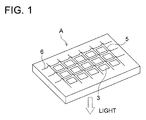
- Fig. 1 is a schematic drawing of a displaying section of a full color display employing an active matrix system.
- the present inventors have made an extensive study on a fluorescent compound used as a host compound of a phosphorescent compound, and have found that there exists some relationship between the luminance of emitted light of an electroluminescent element and a nitrogen atom number to carbon atom number ratio (N/C) in a molecule of the host compound contained in the electroluminescent element.
- N/C nitrogen atom number to carbon atom number ratio
- a host compound having a relatively low N/C increases the emitted light luminance.
- the emitted light luminance is restricted by some action of the nitrogen atom which is contained in the molecule of a host compound having a relatively high N/C. Accordingly, in order to increase emitted light luminance of an organic electroluminescent element employing a phosphorescent compound as a dopant, it is effective to reduce an N/C of the phosphorescent compound.
- the fluorescent compound is a compound in which light is emitted through light excited singlet state in which two electron spins are in reversely parallel with each other
- the phosphorescent compound is a compound in which light is emitted through light excited triplet state in which two electron spins are in parallel with each other.
- the phosphorescent compound in the invention is considered to form exited triplet state at room temperature (from 15 to 30° C) through energy transfer from the exited singlet state or excited triplet state of the fluorescent compound described above.
- Phosphorescent compounds have been considered to be capable of emitting phosphoresce only at a low temperature such as 77° K.
- the maximum fluorescence wavelength of the fluorescent compound as a host compound is a wavelength giving the maximum fluorescent intensity in the fluorescent spectra of a 100 nm thick layer of the fluorescent compound deposited on a glass plate.
- the organic electroluminescent element comprising a light emission layer containing a phosphorescent compound and a fluorescent compound having a nitrogen atom number/carbon atom number ratio (N/C) in the molecule of from 0 to 0.05 emits light with high luminance.
- the fluorescent compound as a host compound which is used in combination with a phosphorescent compound, is preferably a compound having in its molecule an N/C of from 0 to 0.05.
- a fluorescent compound as a host compound having in the molecule an N/C of from 0 to 0.03 is preferably used in combination with a phosphorescent compound in that lifetime of emitted light is longer.
- a host compound having a nitrogen atom is preferable but the use of a host compound having an N/C not less than a certain value restricts the lifetime due to some action of the nitrogen atom.
- the phosphorescent maximum wavelength of the phosphorescent compound as a dopant contained in the light emission layer is longer than the maximum fluorescence wavelength of the fluorescent compound as a host compound, whereby an organic electroluminescence (EL) element can be obtained which employs light emission due to excited triplet of the phosphorescent compound as a dopant.
- the organic electroluminescent element of the invention emits light with an electroluminescent maximum wavelength longer than the maximum fluorescence wavelength of the fluorescent compound (a wavelength giving the maximum fluorescent intensity which is determined from the fluorescent spectra of a layer of the fluorescent compound which is deposited on a glass plate to give a thickness of 100 nm).
- the maximum fluorescence wavelength of the fluorescent compound used as a host compound is in the range of preferably from 350 to 440 nm, and more preferably from 390 to 410 nm.
- a lower organic compound is poor in thermal stability due to its low molecular weight, and may not emit light with sufficiently high luminance.
- the molecular weight of the fluorescent compound as a host compound of the phosphorescent compound is preferably not less than 600 in view of thermal stability.
- the phosphorescent quantum yield of the phosphorescent compound at 25° C in its solution is preferably not less than 0.001, more preferably not less than 0.01, and most preferably not less than 0.1.
- the steric parameter Es of the substituent is a substitution constant defined by Taft and described in, for example, "Relation between Structure and Activity of Medicine" extra issue No. 122, Konando.
- the light emission layer will be detailed below.
- the light emission layer herein refers to a layer emitting light when electric current is supplied to an electrode comprised of a cathode and an anode.
- the light emission layer is a fluorescent compound-containing layer emitting light when electric current is supplied to an electrode comprised of a cathode and an anode.
- the organic electroluminescent element (EL element) basically has a structure in which a light emission layer is put between a pair of electrodes.
- the organic EL element of the invention has a structure in which in addition to the light emission layer, a hole transporting layer, an electron transporting layer, an anode buffer layer or a cathode buffer layer is optionally provided between a cathode and an anode.
- the light emission layer is preferably a molecular deposit layer.
- the molecular deposit layer herein refers to a layer formed by deposition of the above compounds in a gaseous state, or to a layer formed by solidification of the compounds in a melted state or a liquefied state.
- the molecular deposit layer is distinguished from a thin layer (molecular cumulation layer) formed by an LB method by a structural difference, for example, an aggregated structure or a higher order structure, or a functional difference resulting from the structural difference.
- the light emission layer can be formed by the method such as that described in Japanese Patent O.P.I. Publication No. 57-51781, by which the above compound as a light emission material is dissolved in a solvent together with a binder such as a resin, and the thus obtained solution is formed into a thin layer by a method such as a spin-coat method. Thickness of the emission layer thus formed is not specially restricted. Although the thickness of the layer thus formed is optionally selected, the thickness is preferably within the range of from 5 nm to 5 ⁇ m.
- the phosphorescent compound in the invention is concretely a heavy metal complex compound, preferably a metal complex compound containing a metal belonging to a group VIII of the periodic table, and more preferably a metal complex compound containing osmium, iridium or platinum.
- the phosphorescent compound has a phosphorescent quantum yield in the solution at 25° C of preferably not less than 0.001 at 25° C, as described above, and has a maximum phosphorescence wavelength longer than a maximum fluorescence wavelength of a fluorescent compound as a host compound.
- a phosphorescent quantum yield in the solution at 25° C preferably not less than 0.001 at 25° C, as described above, and has a maximum phosphorescence wavelength longer than a maximum fluorescence wavelength of a fluorescent compound as a host compound.
- an EL element can be obtained which emits electroluminescence light having wavelengths longer than a maximum fluorescence wavelength of the fluorescent compound.
- the maximum phosphorescence wavelength of the phosphorescent compound used is not specifically limited, but the wavelength of emitted light can be theoretically varied selecting a center metal, a ligand or a substituent of the ligand contained in the phosphorescent compound.
- an EL element employing a fluorescent compound having a maximum fluorescent wavelength in the range of from 350 to 440 nm as a host compound, and an iridium complex compound having a phosphorescent light in a green region, an EL element can be obtained which emits electroluminescence light in the green region.
- Examples of the phosphorescent compound used in the invention will be listed below, but are not limited thereto. These compounds can be synthesized according to a method described in for example, Inorg. Chem. 40, 1704-1711.
- an organic electroluminescent element comprising, in addition to a fluorescent compound (A) as a host compound and a phosphorescent compound, a fluorescent compound (B) having a phosphorescent maximum wavelength in the wavelength region longer than the maximum wavelength of light emitted by the phosphorescent compound.
- the electroluminescence of the EL element is emitted from the fluorescent compound (B) to which energy is transferred from the fluorescent compound (A) and the phosphorescent compound.
- the fluorescent compound (B) preferably has a high quantum yield in the form of solution.
- the quantum yield is preferably not less than 10%, and more preferably not less than 30%.
- Examples of the fluorescent compound (B) include a qumarine dye, a cyanine dye, a chloconium dye, a squalenium dye, an oxobenzanthracene dye, a fluorescene dye, a rhodamine dye, a pyrylium dye, a perylene dye, a stilbene dye, a polythiophene dye, and a fluorescent compound of a rare earth element complex type.
- the fluorescent quantum yield herein can be measured according to a method described in the fourth edition, Jikken Kagaku Koza 7, Bunko II, p. 362 (1992) (published by Maruzen).
- tetrahydrofuran is employed as a solvent for measurement.
- a fluorescent compound having a nitrogen atom number-to-carbon atom number ratio (N/C) in the molecule of from 0 to 0.05, is used as a host compound in combination with a phosphorescent compound.
- N/C nitrogen atom number-to-carbon atom number ratio
- This can provide an organic EL element having a high luminance and a long emission lifetime, but from another viewpoint, it is useful in the invention to employ the compounds represented by formulae (I) through (V) as a host compound which is used in combination with the phosphorescent compound.
- n is an integer of from 0 to 3
- R 1 and R 2 independently represent a substituent.
- the substituent is preferably an alkyl group such as a methyl group, an ethyl group, an i-propyl group, a hydroxyethyl group, a methoxymethyl group, a trifluoromethyl group and a t-butyl group, a halogen atom such as a fluorine atom and a chlorine atom, or an alkoxy group such as a methoxy group, an ethoxy group, an i-propoxy group and a butoxy group.
- Ar represents an aromatic hydrocarbon ring or an aromatic heterocyclic ring, provided that each may have a substituent, and preferably represents a naphthyl group, a binaphthyl group, a quinolyl group, an iso-quinolyl group, a benzoxazolyl group and a benzimidazolyl group, when n are an integer of 2 or more, plural R 1 s and R 2 s each may be the same or different.
- n4, n5 and n6 independently represent an integer of from 0 to 7.
- R 6 , R 7 and R 8 independently represent a substituent selected from an alkyl group, a cycloalkyl group, an aryl group, a halogen atom, an alkoxy group, an aryloxy group and a heterocyclic group; and a methyl group and a naphthyl group are particularly preferred.
- n4 and n6 each are an integer of 2 or more, plural R 6 s, R 7 s, and R 8 s each may be the same or different.
- R 11 through R 16 , and X 1 through X 9 independently represent a hydrogen atom or a substituent, and may be the same or different, provided that the sum of Es R11 through Es R16 , which represent the steric parameter of R 11 through R 16 , respectively, satisfies the following expression: Es R11 + Es R12 + Es R13 + Es R14 + Es R15 + Es R16 ⁇ -2.0;
- the adjacent substituents may be condensed with each other to form a ring structure.
- the substituents represented by R 11 through R 16 are preferably a methyl group, an ethyl group, an isopropyl group, a t-butyl group or a trifluoromethyl group.
- the substituents represented by X 1 through X 9 are preferably an alkyl group, an aryl group, a heterocyclic group, a halogen atom, an alkoxy group and an amino group.
- X 2 , X 5 and X 8 each are preferably an aryl group or an amino group, and especially preferably a diarylamino group.
- R 101 through R 128 independently represent a hydrogen atom or a substituent, provided that at least one of R 101 through R 104 represents a substituent.
- the substituent is preferably an alkyl group (for example, a methyl group, an ethyl group, an i-propyl group, a hydroxyethyl group, a methoxymethyl group, a trifluoromethyl group, a perfluoropropyl group, a perfluoro-n-butyl group, a perfluoro-t-butyl group, or a t-butyl group); a cycloalkyl group (for example, a cyclopentyl group and a cyclohexyl group); an aralkyl group (for example, a benzyl group and a 2-phenetyl group); an aryl group (for example, as a phenyl group, a naph
- the foregoing groups further may have a substituent, examples of which include a hydrogen atom, a halogen atom, a trifluoromethyl group, an alkyl group, an aryl group, an alkoxy group, an aryloxy group, an alkylthio group, a dialkylamino group, a dibenzylamino group, and a diarylamino group.
- a substituent examples of which include a hydrogen atom, a halogen atom, a trifluoromethyl group, an alkyl group, an aryl group, an alkoxy group, an aryloxy group, an alkylthio group, a dialkylamino group, a dibenzylamino group, and a diarylamino group.
- the substituent represented by R 101 through R 104 is preferably an alkyl group, and two or four substituents of R 101 through R 104 are more preferably methyl groups.
- R 201 , R 202 , R 203 , R 204 , R 205 , and R 206 independently represent a hydrogen atom, or a substituent.
- the substituent is preferably those denoted in R 101 through R 128 above, more preferably a substituted or unsubstituted aryl group, and most preferably substituted or unsubstituted phenyl group.
- compounds having a nitrogen atom number-to-carbon atom number ratio (N/C) in the molecule of not more than 0.05 are preferable, and compounds having a nitrogen atom number-to-carbon atom number ratio (N/C) in the molecule of not more than 0.03 are more preferable.
- N/C nitrogen atom number-to-carbon atom number ratio
- Color of light emitted from the fluorescent compound according to the invention is measured by a spectral light meter CS-1000, manufactured by Minolta Co., Ltd., and expressed according to CIE chromaticity diagram described in Fig. 4.16 on page 108 of "Shinpen Shikisai Kagaku Handbook” (Coloring Science Handbook, New Edition), edited by Nihon Shikisai Gakkai, published by Todai Shuppan Kai.
- Tg glass transition point
- the molecular weight of the compounds represented by formulae (I) through (V) is in the range of preferably from 600 to 5000.
- the compounds having the molecular weight of such a range can provide a light emission layer capable of being easily formed by an vacuum deposition method, and therefore, an organic EL element can be easily manufactured. Further, thermal stability of the fluorescent compound in the organic EL element is higher.
- Layers such as a hole injecting layer, a hole transporting layer, an electron injecting layer and an electron transporting layer other than the light emission layer, which constitute the organic EL element, will be explained below.
- a hole injecting layer or a hole transporting layer has a function of transporting the positive hole injected from the anode to the light emission layer.
- Many positive holes can be injected in a lower electric field by the presence of the hole injecting layer or the hole transporting layer between the anode and the light emission layer.
- an element can be obtained which increases a light emission efficiency and has an excellent light emission ability, since the electrons injected into the light emission layer from the cathode, the electron injecting layer or the electron transporting layer are accumulated at the interface in the light emission layer by a barrier to electrons existing at the interface between the light emission layer and the hole injecting layer or the hole transporting layer.
- the material for the hole injecting layer and the hole transporting layer (hereinafter referred to also as a hole injecting material and a hole transporting material, respectively) can be optionally selected from known materials without any limitation as far as they have a function capable of transporting the positive hole injected from the anode to the light emission layer.
- Such materials include those employed for hole transporting materials in conventional photoconductive elements or known materials used in the hole injecting layer or hole transporting layer of conventional EL elements.
- the hole injecting material or the hole transporting material describe above may be either an organic substance or an inorganic substance as long as it has a hole injecting ability, a hole transporting ability or an ability to form a barrier to electron.
- Examples of the hole injecting material or the hole transporting material include a triazole derivative, an oxadiazole derivative, an imidazole derivative, a polyarylalkane derivative, a pyrazoline derivative and a pyrazolone derivative, a phenylenediamine derivative, an arylamine derivative, an amino substituted chalcone derivative, an oxazole derivative, a styryl anthracene derivative, a fluorenone derivative, a hydrazone derivative, a stilbene derivative, a silazane derivative, an aniline copolymer, and an electroconductive oligomer , particularly a thiophene oligomer.
- hole injecting material or the hole transporting material those described above are used, but a porphyrin compound, an aromatic tertiary amine compound, or a styrylamine compound is preferably used, and an aromatic tertiary amine compound is more preferably used.
- aromatic tertiary amine compound and styrylamine compound include N,N,N',N'-tetraphenyl-4,4'-diaminophenyl, N,N'-diphenyl-N,N'-bis(3-methylphenyl)-[1,1'-biphenyl]-4,4'-diamine (TPD), 2,2'-bis(4-di-p-tolylaminophenyl)propane, 1,1'-bis(4-di-p-tolylaminophenyl)cyclohexane, N,N,N',N'-tetra-p-tolyl-4,4'-diaminobiphenyl, 1,1'-bis(4-di-p-tolylaminophenyl)-4-phenylcyclohexane, bis(4-dimethylamino-2-methylphenyl)-phenylmethane, bis(4-di-
- 5,061,569 which have two condensed aromatic rings in the molecule thereof such as 4,4'-bis[N-(1-naphthyl)-N-phenylamino]biphenyl (NPD), and compounds described in Japanese Patent O.P.I. Publication No. 4-308688 such as 4,4',4''-tris[N-(3-methylphenyl)-N-phenylamino]-triphenylamine (MTDATA) in which three triphenylamine units are bonded in a starburst form.
- NPD 4,4'-bis[N-(1-naphthyl)-N-phenylamino]biphenyl
- MTDATA 4,4',4''-tris[N-(3-methylphenyl)-N-phenylamino]-triphenylamine
- a polymer in which the material mentioned above is introduced in the polymer chain or a polymer having the material as the polymer main chain can be also used.
- the hole injecting layer or hole transporting layer can be formed by layering the hole injecting material or the hole transporting material by a known method such as a vacuum deposition method, a spin coat method a casting method and an LB method.
- the thickness of the hole injecting layer or the hole transporting layer is not specifically limited, but is ordinarily from 5 nm to 5 ⁇ m.
- the hole injecting layer or the hole transporting layer may be composed of a single layer structure comprising one or two or more of the materials mentioned above, or of plural layers comprising the same composition or different composition.
- An electron transporting layer which is provided according to necessity is a layer having a function of transporting electrons injected to the cathode to the light emission layer.
- the material for the electron transporting layer may be optionally selected from known compounds.
- Examples of the material used in the electron transporting layer include a nitro-substituted fluorene derivative, a diphenylquinone derivative, a thiopyran dioxide derivative, a heterocyclic tetracarboxylic acid anhydride such as naphthaleneperylene, a carbodiimide, a fluolenylidenemethane derivative, an anthraquinodimethane an anthrone derivative, and an oxadiazole derivative.
- electron transporting material examples include a nitro-substituted fluorene derivative, a diphenylquinone derivative, a thiopyran dioxide derivative, a heterocyclic tetracarboxylic acid anhydride such as naphthaleneperylene, a carbodiimide, a fluolenylidenemethane derivative, an anthraquinodimethane an anthrone derivative, and an oxadiazole derivative.
- thiadiazole derivative which is formed by substituting the oxygen atom in the oxadiazole ring of the foregoing oxadiazole derivative with a sulfur atom
- a quinoxaline derivative having a quinoxaline ring known as an electron withdrawing group are usable as the electron transporting material.
- a polymer in which the material mentioned above is introduced in the polymer chain or a polymer having the material as the polymer main chain can be also used.
- a metal complex of an 8-quinolynol derivative such as aluminum tris-(8-quinolynol) (Alq 3 ), aluminum tris-(5,7-dichloro-8-quinolynol), aluminum tris-(5,7-dibromo-8-quinolynol), aluminum tris-(2-methyl-8-quinolynol), aluminum tris-(5-methyl-8-quinolynol), or zinc bis-(8-quinolynol) (Znq), and a metal complex formed by replacing the center metal of the foregoing complexes with another metal atom such as In, Mg, Cu, Ca, Sn, Ga or Pb, can be used as the electron transporting material.
- Alq 3 aluminum tris-(5,7-dichloro-8-quinolynol), aluminum tris-(5,7-dibromo-8-quinolynol), aluminum tris-(2-methyl-8-quinolynol), aluminum tris-(5-methyl-8-quinolynol
- a metal free or metal-containing phthalocyanine, and a derivative thereof, in which the molecular terminal is replaced by a substituent such as an alkyl group or a sulfonic acid group are also preferably used as the electron transporting material.
- the distyrylpyrazine derivative exemplified as a material for an light emission layer may preferably be employed as the electron transporting material.
- An inorganic semiconductor such as n-Si and n-SiC may also be used as the electron transporting material in a similar way as in the hole injecting layer or in the hole transporting layer.
- the electron transporting layer can be formed by layering the compounds described above by a known method such as a vacuum deposition method, a spin coat method, a casting method and an LB method.
- the thickness of the electron transporting layer is not specifically limited, but is ordinarily from 5 nm to 5 ⁇ m.
- the electron transporting layer may be composed of a single layer structure comprising one or two or more of the materials mentioned above, or of plural layers comprising the same composition or different composition.
- the light emission layer contains the fluorescent compound, but a positive hole or electron transporting layer adjacent to the light emission layer may contain one or more kinds of fluorescent compounds having a maximum fluorescence wavelength in the same regions as the fluorescent compound as a host compound of the phosphorescent compound described above, whereby an emission efficiency of the EL element can be increased.
- the fluorescent compound which may be contained in the hole or electron transporting layer, is a fluorescent compound having the maximum fluorescence wavelength in the region of from 350 to 440 nm, and preferably 390 to 410 nm, as the fluorescent compound contained in the light emission layer.
- a substrate preferably employed for the organic electroluminescent element of the invention is not restricted to specific kinds of materials such as glass and plastic, as far as it is transparent.
- Examples of the substrate preferably employed used in the organic electroluminescent element of the invention include glass, quartz and light transmissible plastic film.
- Examples of the light transmissible plastic film include films such as polyethyleneterephthalate (PET), polyethylenenaphthalate (PEN), polyethersulfone (PES), polyetherimide, polyetheretherketone, polyphenylenesulfide, polyarylate, polycarbonate (PC), cellulose triacetate (TAC), cellulose acetate propionate (CAP) and so on.
- PET polyethyleneterephthalate
- PEN polyethylenenaphthalate
- PES polyethersulfone
- PES polyetherimide
- polyetheretherketone polyphenylenesulfide
- PC polycarbonate
- TAC cellulose triacetate
- CAP cellulose acetate propionate
- a thin layer of a desired material for electrode such as a material for an anode is formed on a suitable substrate by a deposition or spattering method, so that the thickness of the layer is not more than 1 ⁇ m, and preferably within the range of from 10 to 200 nm to prepare the anode. Then the hole injecting layer, the hole transporting layer, the light emission layer, the electron transporting layer and the electron injecting layer, which constitute the element, are formed on the resulting anode in that order.
- a buffer layer (an electrode interface layer) may be provided between the anode and the light emission layer or the hole injecting layer, or between the cathode and the light emission layer or the electron injecting layer.
- the buffer layer is a layer provided between the electrode and an organic layer in order to reduce the driving voltage or to improve of light emission efficiency.
- As the buffer layer there are an anode buffer layer and a cathode buffer layer, which are described in "Electrode Material” page 123, Div. 2 Chapter 2 of "Organic EL element and its frontier of industrialization” (published by NTS Corporation, November 30, 1998) in detail.
- the anode buffer layer is described in Japanese Patent O.P.I. Publication Nos. 9-45479, 9-260062, and 8-288069 etc., and its examples include a phthalocyanine buffer layer represented by a copper phthalocyanine layer, an oxide buffer layer represented by a vanadium oxide layer, an amorphous carbon buffer layer, a polymer buffer layer employing an electroconductive polymer such as polyaniline (emeraldine), and polythiophene, etc.
- the cathode buffer layer is described in Japanese Patent O.P.I. Publication Nos. 6-325871, 9-17574, and 9-74586, etc. in detail, and its examples include a metal buffer layer represented by a strontium or aluminum layer, an alkali metal compound buffer layer represented by a lithium fluoride layer, an alkali earth metal compound buffer layer represented by a magnesium fluoride layer, and an oxide buffer layer represented by an aluminum oxide or lithium oxide layer.
- the buffer layer is preferably very thin and has a thickness of preferably from 0.1 to 100 nm depending on kinds of the material used.
- a layer having another function may be provided if necessary in addition to the fundamental configuration layers as described above, for example a hole blocking layer may be added as described in Japanese Patent O.P.I. Publication Nos. 11-204258, and 11-204359, and on page 237 of "Organic EL element and its frontier of industrialization” (published by NTS Corporation, November 30, 1998).
- At least one of the cathode buffer layer and anode buffer layer may contain the compound in the invention, and may function as a light emission layer.
- Electrodes of the organic EL element will be explained below.
- the electrodes consist of a cathode and an anode.
- a metal, an alloy, or an electroconductive compound each having a high working function (not less than 4 eV), and mixture thereof are preferably used as the electrode material.
- an electrode material include a metal such as Au, and a transparent electroconductive material such as CuI, indium tin oxide (ITO), SnO 2 , or ZnO.
- the anode may be prepared by forming a thin layer of the electrode material according to a depositing or spattering method, and by forming the layer into a desired pattern according to a photolithographic method.
- the pattern may be formed by depositing or spattering of the electrode material through a mask having a desired form.
- the transmittance of the anode is preferably 10% or more, and the sheet resistivity of the anode is preferably not more than several hundred ⁇ / ⁇ .
- the thickness of the layer is ordinarily within the range of from 10 nm to 1 ⁇ m, and preferably from 10 to 200 nm, although it may vary due to kinds of materials used.
- a metal also referred to as an electron injecting metal
- an alloy also referred to as an electron injecting metal
- an electroconductive compound each having a low working function not more than 4 eV
- a mixture thereof is used as the electrode material.
- an electrode material include sodium, sodium-potassium alloy, magnesium, lithium, a magnesium/copper mixture, a magnesium/silver mixture, a magnesium/aluminum mixture, magnesium/indium mixture, an aluminum/aluminum oxide (Al 2 O 3 ) mixture, indium, a lithium/aluminum mixture, and a rare-earth metal.
- a mixture of an electron injecting metal and a metal higher in the working function than that of the electron injecting metal such as the magnesium/silver mixture, magnesium/aluminum mixture, magnesium/indium mixture, aluminum/aluminum oxide (Al 2 O 3 ) mixture or lithium/aluminum mixture, is suitable from the view point of the electron injecting ability and resistance to oxidation.
- the cathode can be prepared forming a thin layer of such an electrode material by a method such as a deposition or spattering method.
- the sheet resistivity as the cathode is preferably not more than several hundred ⁇ / ⁇ , and the thickness of the layer is ordinarily from 10 nm to 1 ⁇ m, and preferably from 50 to 200 nm. It is preferable in increasing the light emission efficiency that either the anode or the cathode of the organic EL element is transparent or semi-transparent.
- a vacuum deposition method is preferably used even though a spin coating method, a casting method and a deposition method can be used.
- the vacuum deposition method is preferable since a uniform layer can be formed and a pinhole is formed with difficulty.
- the vacuum deposition is preferably carried out at a boat temperature of from 50° C to 450° C, at a vacuum degree of from 10 -6 to 10 -3 Pa, at a deposition speed of from 0.01 to 50 nm/second, and at a substrate temperature of from -50 to 300° C, to form a layer thickness of from 5 nm to 5 ⁇ m.
- a thin layer of a desired electrode material such as an anode material is formed by a deposition or spattering method so that the thickness of the layer is not more than 1 ⁇ m, preferably within the range of from 10 to 200 nm to prepare the anode. Then the hole injecting layer, the hole transporting layer, the light emission layer and the electron transporting layer and the electron injecting layer are formed on the anode as described above. After formation of these layers, a thin layer comprising a material for cathode is formed thereon by, for example, a deposition method or spattering method so that the thickness is not more than 1 ⁇ m, and preferably from 50 to 200 nm, to provide the cathode.
- the layers from the hole injecting layer to the cathode are continuously formed under one time of vacuuming to prepare the organic EL element.
- the organic EL element can be prepared in the reverse order, in which the cathode, the electron injecting layer, the light emission layer, hole injecting layer, and the anode are formed in that order.
- Light emission can be observed when a direct current with a voltage of from about 5 to 40 V is applied to the thus prepared organic EL element so that the polarity of the anode is positive and that of the cathode is negative.
- the voltage is applied in the reverse polarity, no current is generated and light is not emitted at all.
- an alternating voltage is applied, light is emitted only when the polarity of the anode is positive and that of the cathode is negative.
- the shape of the wave of the alternating current may be optionally selected.
- Electroluminescence element sample Nos. 1-1 through 1-22 were prepared according to the following procedures:
- a pattern was formed on a substrate (manufactured by NH Technoglass Co., Ltd.) composed of a glass plate (100 mm x 1000 mm x 1.1 mm) and a 150 nm ITO (indium tin oxide) layer as an anode. Then the resulting transparent substrate having the ITO transparent electrode was subjected to ultrasonic washing in i-propyl alcohol and dried by a dry nitrogen gas and subjected to UV-ozone cleaning for 5 minutes.
- a substrate manufactured by NH Technoglass Co., Ltd.
- ITO indium tin oxide
- transparent substrate was fixed on a substrate holder of a vacuum deposition apparatus available in the market. Further, 200 mg of ⁇ -NPD were put in a first resistive heating molybdenum boat, 200 mg of CBP were put in a second resistive heating molybdenum boat, 200 mg of bathocuproine (BC) were put in a third resistive heating molybdenum boat, 200 mg of Ir-1 (phosphorescent compound) were put in a fourth resistive heating molybdenum boat, and 200 mg of Alq 3 were put in a fifth resistive heating molybdenum boat, and the resulting boats were set in the vacuum deposition apparatus.
- ⁇ -NPD were put in a first resistive heating molybdenum boat
- 200 mg of CBP were put in a second resistive heating molybdenum boat
- 200 mg of bathocuproine (BC) were put in a third resistive heating molybdenum boat
- 200 mg of Ir-1 (phosphorescent compound) were put in a fourth resist
- the pressure in the vacuum tank was reduced to 4 x 10 -4 Pa, and the boat carrying ⁇ -NPD was heated to 220° C by supplying an electric current to the boat so as to form a hole transporting layer having a thickness of 45 nm by depositing ⁇ -NPD onto the transparent substrate at a depositing speed of 0.1 nm/sec.
- the boat carrying CBP and the boat carrying Ir-1 were heated to 220° C by supplying an electric current to both boats so as to co-deposit the CBP at a depositing speed of 0.01 nm/sec and the Ir-1 at a depositing speed of 0.1 nm/sec onto the hole transporting layer to form a light emission layer of 20 nm.
- the temperature of the substrate at the time of the deposition was room temperature.
- the boat carrying BC was heated to 250° C by supplying an electric current to the boat so as to deposit the BC onto the light emission layer at a depositing speed of 0.1 nm/sec to form an electron transporting layer of 10 nm which could function as a hole blocking layer.
- the boat carrying Alq 3 was heated to 250° C by supplying an electric current to the boat so as to deposit the Alq 3 onto the electron transporting layer at a depositing speed of 0.1 nm/sec to form an electron transporting layer of 40 nm.
- the temperature of the substrate at the time of the deposition was room temperature.
- the vacuum tank was opened, and a stainless steel mask having a rectangular hole was set on the electron transporting layer. Further, 3 g of magnesium was put in a molybdenum resistive heating boat and 0.5 g of silver was put in a tungsten basket for deposition. The boat and the basket were set in the vacuum tank. The pressure in the vacuum tank was reduced to 2 X 10 -4 Pa. Then the boat carrying magnesium was heated by supplying an electric current so as to deposit magnesium at a deposition speed of from 1.5 to 2.0 nm/sec. At this time, the basket carrying silver was simultaneously heated so as to deposit silver at a deposition speed of 0.1 nm/sec to form a counter electrode composed of a mixture of magnesium and silver. Thus a comparative organic EL element sample No. 1-1 was prepared.
- Organic EL element sample Nos. 1-2 through 1-22 were prepared in the same manner as comparative organic EL element sample No. 1-1, except that CBP and the phosphorescent compound in the light emission layer were replaced with those as shown in Table 2.
- inventive organic electroluminescence element samples comprising a light emission layer containing the compounds in the invention emits light with high luminance.
- inventive samples have proved to be useful for an organic EL element, and the following three are pointed out.
- the phosphorescent quantum yields of phosphorescent compounds Ir-1, 2, 3, 5, 8, and 9 in 25° C tetrahydrofuran was 0.36, 0.32, 0.27, 0.12, 0.34, and 0.21, respectively.
- the maximum fluorescence wavelength of the fluorescent compound as a host compound is a wavelength giving the maximum fluorescent intensity in the fluorescent spectra of a 100 nm thick layer of the fluorescent compound deposited on a glass plate.
- Organic EL element sample Nos. 2-1 through 2-21 were prepared in the same manner as in organic EL element sample Nos. 1-1 through 1-21 in Example 1, respectively, except that ⁇ -NPD (having a maximum fluorescence wavelength of 452 nm) as a hole transporting material was replaced with m-MTDATXA (having a maximum fluorescence wavelength of 399 nm). The resulting element samples exhibited more increased luminance.
- ⁇ -NPD having a maximum fluorescence wavelength of 452 nm
- m-MTDATXA having a maximum fluorescence wavelength of 399 nm
- Organic EL element sample Nos. 3-1 through 3-21 were prepared in the same manner as in organic EL element sample Nos. 1-1 through 1-21 in Example 1, respectively, except that the cathode was replaced with Al, and a LiF-deposited cathode buffer layer with a thickness of 0.5 nm was provided between the cathode and the electron transporting layer.
- the luminance of emitted light from the sample was measured according to CS-1000 produced Minolta Co., Ltd. in the same manner as in Example 1.
- the luminance of the organic EL element sample No. 1-8 was set at 100, the relative value of the luminance of the organic EL element sample No. 3-8 was 142.
- introduction of the cathode buffer layer was proved to be effective in the other organic EL element samples prepared above.
- Organic EL element sample Nos. 4-1 and 4-2 were prepared in the same manner as in organic EL element sample Nos. 1-1 and 1-8 in Example 1, respectively, except that Ir-1 was replaced with Pt-3 ⁇ 2,3,7,8,12,13,17,18-octaethyl-21H-Porphyrin platinum (II) (PtOEP), produced by Porphyrin Products Co., Ltd. ⁇ .
- II PtOEP
- Organic EL element sample Nos. 4-3 and 4-4 were prepared in the same manner as in organic EL element sample Nos. 1-1 and 1-7 in Example 1, respectively, except that Ir-1 was replaced with Pt-2.
- a red light was emitted from the sample employing Pt-3, and a blue light was emitted from the sample employing Pt-2.
- Organic EL element sample No. 5-1 was prepared in the same manner as in Example 1, except that the light emission layer was replaced with a light emission layer having a thickness of 10 nm in which the respective five layers of a 1 nm thick layer containing fluorescent compound (7) and 1% by weight of DCM2 (light emission layer A) and a 1 nm thick layer containing compound (7) and 10% by weight of Ir-1 (light emission layer B) were alternately layered.
- a 590 nm light was emitted from DCM2 contained in the organic EL element sample No. 5-1.
- Organic EL element sample No. 5-2 was prepared in the same manner as organic EL element sample No. 5-1 above, except that the fluorescent compound (7) was replaced with CBP. A 590 nm light was also emitted from DCM2 contained in the organic EL element sample No. 5-2, but its luminance was 0.60 times that of the organic EL element sample No. 5-1 employing the fluorescent compound (7). As is apparent from the above, the inventive sample provides higher luminance.
- the red light-emitting organic EL element, green light-emitting organic EL element, and blue light-emitting organic EL element prepared in Examples 1 and 4 were arranged on the same substrate, and a full color display as shown in Fig. 1 was prepared which employed an active matrix system.
- Fig. 1 is a schematic drawing of a displaying section of the full color display prepared.
- the displaying section A has a wiring portion including a plurality of scanning signal lines 5 and a plurality of data signal lines 6, and a plurality of pixels 3 (a red-light emitting pixel, a green-light emitting pixel and a blue-light emitting pixel, etc.) on the same substrate.
- the scanning signal lines 5 and the data signal lines 6 are composed of an electroconductive material.
- the line 5 and the line 6 are crossed with each other at a right angle, and connected with the pixel 3 at the crossing position (not illustrated in detail).
- Organic EL elements corresponding to each of the plural pixels 3 described above are driven by an active matrix system in which a switching transistor as an active element and a driving transistor are provided to each of the organic EL elements.
- the pixels 3 When the scanning signal is applied from the scanning signal line 5, the pixels 3 receive the image data signal from the data signal line 6, and emit light corresponding to the image data.
- a full color image can be displayed by suitably arranging the red-light emitting pixel, green-light emitting pixel and blue-light emitting pixel on the same substrate.
- the full color display prepared above provided a full color moving image with high luminance and high visibility.
- Organic EL element sample Nos. 7-1 through 7-22 were prepared in the same manner as comparative organic EL element sample No. 1-1 in Example 1, except that the compound contained in the light emission layer and the phosphorescent compound were replaced with those as shown in Table 3.
- inventive organic electroluminescence element samples comprising a light emission layer containing the host compound in the invention having an N/C of from more than 0 to less than 0.05 (5%) provides a longer half lifetime (emission lifetime), as compared with the comparative samples, and have proved to be useful for an organic EL element.
- inventive organic electroluminescence element samples comprising a light emission layer containing the host compound in the invention having an N/C of from more than 0 to 0.03 (3%) provides a further longer half lifetime (emission lifetime), and have proved to be especially useful for an organic EL element.
- the present invention provides an organic electroluminescent element emitting light with high emission luminance, and a display employing the organic electroluminescent element which emits the light at reduced power consumption.
Landscapes
- Physics & Mathematics (AREA)
- Spectroscopy & Molecular Physics (AREA)
- Chemical & Material Sciences (AREA)
- Engineering & Computer Science (AREA)
- Materials Engineering (AREA)
- Optics & Photonics (AREA)
- Electroluminescent Light Sources (AREA)
Applications Claiming Priority (2)
| Application Number | Priority Date | Filing Date | Title |
|---|---|---|---|
| JP2001181543 | 2001-06-15 | ||
| JP2001181543 | 2001-06-15 |
Publications (3)
| Publication Number | Publication Date |
|---|---|
| EP1267428A2 true EP1267428A2 (fr) | 2002-12-18 |
| EP1267428A3 EP1267428A3 (fr) | 2007-04-25 |
| EP1267428B1 EP1267428B1 (fr) | 2009-10-14 |
Family
ID=19021795
Family Applications (1)
| Application Number | Title | Priority Date | Filing Date |
|---|---|---|---|
| EP02254090A Expired - Lifetime EP1267428B1 (fr) | 2001-06-15 | 2002-06-12 | Dispositif organique électroluminescent et affichage en couleur |
Country Status (3)
| Country | Link |
|---|---|
| US (2) | US6855438B2 (fr) |
| EP (1) | EP1267428B1 (fr) |
| DE (1) | DE60233997D1 (fr) |
Cited By (3)
| Publication number | Priority date | Publication date | Assignee | Title |
|---|---|---|---|---|
| EP1464691A3 (fr) * | 2003-03-26 | 2008-06-25 | Konica Minolta Holdings, Inc. | Elément organique électroluminescent et dispositif d'éclairage et d'affichage |
| CN102365769A (zh) * | 2009-04-09 | 2012-02-29 | 默克专利有限公司 | 有机电致发光器件 |
| EP3620448A4 (fr) * | 2017-12-26 | 2020-11-04 | Lg Chem, Ltd. | Composé à base d'amine et élément électroluminescent organique le comprenant |
Families Citing this family (15)
| Publication number | Priority date | Publication date | Assignee | Title |
|---|---|---|---|---|
| US6656608B1 (en) * | 1998-12-25 | 2003-12-02 | Konica Corporation | Electroluminescent material, electroluminescent element and color conversion filter |
| US6855438B2 (en) * | 2001-06-15 | 2005-02-15 | Konica Corporation | Organic electroluminescent element and full color display |
| EP2192632B1 (fr) | 2002-04-12 | 2014-09-03 | Konica Corporation | Dispositif organique électroluminescent |
| JP3902981B2 (ja) * | 2002-06-04 | 2007-04-11 | キヤノン株式会社 | 有機発光素子及び表示装置 |
| JP4834286B2 (ja) * | 2002-08-16 | 2011-12-14 | アカデミア シニカ | フラン含有正孔輸送材料 |
| CN100556224C (zh) * | 2003-07-08 | 2009-10-28 | 柯尼卡美能达控股株式会社 | 有机电致发光元件、照明装置及显示装置 |
| TWI230026B (en) * | 2003-12-31 | 2005-03-21 | Ritdisplay Corp | Organic electroluminescent material and organic electroluminescent device by using the same |
| JP2005310441A (ja) * | 2004-04-19 | 2005-11-04 | Idemitsu Kosan Co Ltd | 有機エレクトロルミネッセンス素子 |
| TW200613515A (en) * | 2004-06-26 | 2006-05-01 | Merck Patent Gmbh | Compounds for organic electronic devices |
| US7532181B2 (en) * | 2005-07-20 | 2009-05-12 | Eastman Kodak Company | Visible and invisible image display |
| JP4029897B2 (ja) * | 2005-10-19 | 2008-01-09 | ソニー株式会社 | ジベンゾアントラセン誘導体、有機電界発光素子、および表示装置 |
| US7579773B2 (en) | 2006-06-05 | 2009-08-25 | The Trustees Of Princeton University | Organic light-emitting device with a phosphor-sensitized fluorescent emission layer |
| GB2442724B (en) * | 2006-10-10 | 2009-10-21 | Cdt Oxford Ltd | Light emissive device |
| KR101288128B1 (ko) * | 2006-12-11 | 2013-07-18 | 삼성디스플레이 주식회사 | 금속 프탈로시아닌기를 포함하는 덴드리머 중합체, 그의제조 방법 및 이를 채용한 유기 전계 발광 소자 |
| KR101579490B1 (ko) * | 2015-09-17 | 2015-12-22 | 덕산네오룩스 주식회사 | 유기전기소자용 화합물, 이를 이용한 유기전기소자 및 그 전자 장치 |
Family Cites Families (11)
| Publication number | Priority date | Publication date | Assignee | Title |
|---|---|---|---|---|
| US5972247A (en) * | 1998-03-20 | 1999-10-26 | Eastman Kodak Company | Organic electroluminescent elements for stable blue electroluminescent devices |
| US6656608B1 (en) * | 1998-12-25 | 2003-12-02 | Konica Corporation | Electroluminescent material, electroluminescent element and color conversion filter |
| BRPI0009215B1 (pt) * | 1999-03-23 | 2017-05-09 | Univ Southern California | complexos metálicos ciclometalizados como dopantes fosforescentes em diodos emissores de luz orgânicos |
| JP3949363B2 (ja) * | 1999-10-26 | 2007-07-25 | 富士フイルム株式会社 | 芳香族縮環化合物、発光素子材料およびそれを使用した発光素子 |
| US6660410B2 (en) * | 2000-03-27 | 2003-12-09 | Idemitsu Kosan Co., Ltd. | Organic electroluminescence element |
| US6962755B2 (en) * | 2000-07-17 | 2005-11-08 | Fuji Photo Film Co., Ltd. | Light emitting element and azole compound |
| JP4026740B2 (ja) * | 2000-09-29 | 2007-12-26 | 富士フイルム株式会社 | 有機発光素子材料及びそれを用いた有機発光素子 |
| US6803720B2 (en) * | 2000-12-15 | 2004-10-12 | Universal Display Corporation | Highly stable and efficient OLEDs with a phosphorescent-doped mixed layer architecture |
| DE60134618D1 (de) * | 2000-12-28 | 2008-08-14 | Toshiba Kk | Organische elektrolumineszente Vorrichtung und Anzeigevorrichtung |
| US6998487B2 (en) * | 2001-04-27 | 2006-02-14 | Lg Chem, Ltd. | Double-spiro organic compounds and organic electroluminescent devices using the same |
| US6855438B2 (en) * | 2001-06-15 | 2005-02-15 | Konica Corporation | Organic electroluminescent element and full color display |
-
2002
- 2002-06-10 US US10/167,120 patent/US6855438B2/en not_active Expired - Lifetime
- 2002-06-12 DE DE60233997T patent/DE60233997D1/de not_active Expired - Lifetime
- 2002-06-12 EP EP02254090A patent/EP1267428B1/fr not_active Expired - Lifetime
-
2004
- 2004-10-07 US US10/960,999 patent/US7374829B2/en not_active Expired - Fee Related
Non-Patent Citations (1)
| Title |
|---|
| "Jikken Kagaku Koza 7", vol. II, 1992, MARUZEN, pages: 362 |
Cited By (6)
| Publication number | Priority date | Publication date | Assignee | Title |
|---|---|---|---|---|
| EP1464691A3 (fr) * | 2003-03-26 | 2008-06-25 | Konica Minolta Holdings, Inc. | Elément organique électroluminescent et dispositif d'éclairage et d'affichage |
| US7485376B2 (en) * | 2003-03-26 | 2009-02-03 | Konica Minolta Holdings, Inc. | Organic electroluminescent element, illuminator, and display |
| CN102365769A (zh) * | 2009-04-09 | 2012-02-29 | 默克专利有限公司 | 有机电致发光器件 |
| CN102365769B (zh) * | 2009-04-09 | 2015-12-09 | 默克专利有限公司 | 有机电致发光器件 |
| EP3620448A4 (fr) * | 2017-12-26 | 2020-11-04 | Lg Chem, Ltd. | Composé à base d'amine et élément électroluminescent organique le comprenant |
| US11659764B2 (en) | 2017-12-26 | 2023-05-23 | Lg Chem, Ltd. | Amine based compound and organic light emitting device comprising the same |
Also Published As
| Publication number | Publication date |
|---|---|
| DE60233997D1 (de) | 2009-11-26 |
| US20030091860A1 (en) | 2003-05-15 |
| US20050048319A1 (en) | 2005-03-03 |
| US7374829B2 (en) | 2008-05-20 |
| US6855438B2 (en) | 2005-02-15 |
| EP1267428A3 (fr) | 2007-04-25 |
| EP1267428B1 (fr) | 2009-10-14 |
Similar Documents
| Publication | Publication Date | Title |
|---|---|---|
| US6835473B2 (en) | Organic electroluminescence element and display | |
| US6750608B2 (en) | Organic electroluminescence element and display | |
| JP4036041B2 (ja) | 有機エレクトロルミネッセンス素子及び表示装置 | |
| JP4106974B2 (ja) | 有機エレクトロルミネッセンス素子及び表示装置 | |
| EP2762546B1 (fr) | Élément électroluminescent organique, affichage et illuminateur | |
| JP4483167B2 (ja) | 有機エレクトロルミネッセンス素子および有機エレクトロルミネッセンス素子を有する表示装置 | |
| EP1267428B1 (fr) | Dispositif organique électroluminescent et affichage en couleur | |
| JP4052024B2 (ja) | 有機エレクトロルミネッセンス素子及び表示装置 | |
| JP4300788B2 (ja) | 有機エレクトロルミネッセンス素子および表示装置 | |
| JP2004047443A (ja) | 有機エレクトロルミネッセンス素子及びカラー表示装置 | |
| JP3994799B2 (ja) | 有機エレクトロルミネッセンス素子及び表示装置 | |
| JP4442114B2 (ja) | 有機エレクトロルミネッセンス素子及び表示装置 | |
| JP4103442B2 (ja) | 有機エレクトロルミネッセンス素子および表示装置 | |
| JP4082098B2 (ja) | 有機エレクトロルミネッセンス素子及びフルカラー表示装置 | |
| JP4656111B2 (ja) | 有機エレクトロルミネッセンス素子 | |
| JP4726384B2 (ja) | 有機エレクトロルミネッセンス素子および表示装置 | |
| JP2004047329A (ja) | 有機エレクトロルミネッセンス素子及び表示装置 | |
| JP5040671B2 (ja) | 有機エレクトロルミネッセンス素子および表示装置 | |
| JP4129599B2 (ja) | 有機エレクトロルミネッセンス素子および表示装置 | |
| JP4183016B2 (ja) | 有機エレクトロルミネッセンス素子および表示装置 | |
| JP4962284B2 (ja) | 有機エレクトロルミネッセンス素子及び表示装置 | |
| JP3960133B2 (ja) | 有機エレクトロルミネッセンス素子及び表示装置 | |
| JP4743186B2 (ja) | 有機エレクトロルミネッセンス素子及び表示装置 | |
| JP2004047356A (ja) | 有機エレクトロルミネッセンス素子及び表示装置 |
Legal Events
| Date | Code | Title | Description |
|---|---|---|---|
| PUAI | Public reference made under article 153(3) epc to a published international application that has entered the european phase |
Free format text: ORIGINAL CODE: 0009012 |
|
| AK | Designated contracting states |
Kind code of ref document: A2 Designated state(s): AT BE CH CY DE DK ES FI FR GB GR IE IT LI LU MC NL PT SE TR |
|
| AX | Request for extension of the european patent |
Free format text: AL;LT;LV;MK;RO;SI |
|
| PUAL | Search report despatched |
Free format text: ORIGINAL CODE: 0009013 |
|
| AK | Designated contracting states |
Kind code of ref document: A3 Designated state(s): AT BE CH CY DE DK ES FI FR GB GR IE IT LI LU MC NL PT SE TR |
|
| AX | Request for extension of the european patent |
Extension state: AL LT LV MK RO SI |
|
| 17P | Request for examination filed |
Effective date: 20070928 |
|
| AKX | Designation fees paid |
Designated state(s): DE FR GB |
|
| 17Q | First examination report despatched |
Effective date: 20071220 |
|
| GRAP | Despatch of communication of intention to grant a patent |
Free format text: ORIGINAL CODE: EPIDOSNIGR1 |
|
| RIC1 | Information provided on ipc code assigned before grant |
Ipc: H01L 51/54 20060101ALI20090407BHEP Ipc: H01L 27/32 20060101ALI20090407BHEP Ipc: H01L 51/52 20060101AFI20090407BHEP |
|
| GRAS | Grant fee paid |
Free format text: ORIGINAL CODE: EPIDOSNIGR3 |
|
| GRAA | (expected) grant |
Free format text: ORIGINAL CODE: 0009210 |
|
| AK | Designated contracting states |
Kind code of ref document: B1 Designated state(s): DE FR GB |
|
| REG | Reference to a national code |
Ref country code: GB Ref legal event code: FG4D |
|
| REF | Corresponds to: |
Ref document number: 60233997 Country of ref document: DE Date of ref document: 20091126 Kind code of ref document: P |
|
| PLBE | No opposition filed within time limit |
Free format text: ORIGINAL CODE: 0009261 |
|
| STAA | Information on the status of an ep patent application or granted ep patent |
Free format text: STATUS: NO OPPOSITION FILED WITHIN TIME LIMIT |
|
| 26N | No opposition filed |
Effective date: 20100715 |
|
| REG | Reference to a national code |
Ref country code: FR Ref legal event code: ST Effective date: 20110228 |
|
| PG25 | Lapsed in a contracting state [announced via postgrant information from national office to epo] |
Ref country code: FR Free format text: LAPSE BECAUSE OF NON-PAYMENT OF DUE FEES Effective date: 20100630 |
|
| REG | Reference to a national code |
Ref country code: DE Ref legal event code: R081 Ref document number: 60233997 Country of ref document: DE Owner name: MERCK PATENT GMBH, DE Free format text: FORMER OWNER: KONICA CORP., TOKIO/TOKYO, JP Ref country code: DE Ref legal event code: R082 Ref document number: 60233997 Country of ref document: DE Representative=s name: HENKEL & PARTNER MBB PATENTANWALTSKANZLEI, REC, DE Ref country code: DE Ref legal event code: R081 Ref document number: 60233997 Country of ref document: DE Owner name: KONICA MINOLTA, INC., TOKYO, JP Free format text: FORMER OWNER: KONICA CORP., TOKIO/TOKYO, JP |
|
| PGFP | Annual fee paid to national office [announced via postgrant information from national office to epo] |
Ref country code: DE Payment date: 20210518 Year of fee payment: 20 |
|
| PGFP | Annual fee paid to national office [announced via postgrant information from national office to epo] |
Ref country code: GB Payment date: 20210519 Year of fee payment: 20 |
|
| REG | Reference to a national code |
Ref country code: DE Ref legal event code: R081 Ref document number: 60233997 Country of ref document: DE Owner name: MERCK PATENT GMBH, DE Free format text: FORMER OWNER: KONICA MINOLTA, INC., TOKYO, CHIYODA-KU, JP Ref country code: DE Ref legal event code: R081 Ref document number: 60233997 Country of ref document: DE Owner name: MERCK PATENT GMBH, DE Free format text: FORMER OWNER: MERCK PERFORMANCE MATERIALS GERMANY GMBH, 64293 DARMSTADT, DE Ref country code: DE Ref legal event code: R082 Ref document number: 60233997 Country of ref document: DE |
|
| REG | Reference to a national code |
Ref country code: GB Ref legal event code: 732E Free format text: REGISTERED BETWEEN 20220217 AND 20220223 |
|
| REG | Reference to a national code |
Ref country code: DE Ref legal event code: R071 Ref document number: 60233997 Country of ref document: DE |
|
| REG | Reference to a national code |
Ref country code: GB Ref legal event code: PE20 Expiry date: 20220611 |
|
| PG25 | Lapsed in a contracting state [announced via postgrant information from national office to epo] |
Ref country code: GB Free format text: LAPSE BECAUSE OF EXPIRATION OF PROTECTION Effective date: 20220611 |