EP1267440A2 - Antennenelement mit auf äusseren Oberflächen eines Substratkörpers geformten Leitern - Google Patents
Antennenelement mit auf äusseren Oberflächen eines Substratkörpers geformten Leitern Download PDFInfo
- Publication number
- EP1267440A2 EP1267440A2 EP02009597A EP02009597A EP1267440A2 EP 1267440 A2 EP1267440 A2 EP 1267440A2 EP 02009597 A EP02009597 A EP 02009597A EP 02009597 A EP02009597 A EP 02009597A EP 1267440 A2 EP1267440 A2 EP 1267440A2
- Authority
- EP
- European Patent Office
- Prior art keywords
- conductor
- conductive line
- power supply
- ground
- antenna apparatus
- Prior art date
- Legal status (The legal status is an assumption and is not a legal conclusion. Google has not performed a legal analysis and makes no representation as to the accuracy of the status listed.)
- Withdrawn
Links
Images



Classifications
-
- H—ELECTRICITY
- H01—ELECTRIC ELEMENTS
- H01Q—ANTENNAS, i.e. RADIO AERIALS
- H01Q1/00—Details of, or arrangements associated with, antennas
- H01Q1/36—Structural form of radiating elements, e.g. cone, spiral, umbrella; Particular materials used therewith
- H01Q1/38—Structural form of radiating elements, e.g. cone, spiral, umbrella; Particular materials used therewith formed by a conductive layer on an insulating support
-
- H—ELECTRICITY
- H01—ELECTRIC ELEMENTS
- H01Q—ANTENNAS, i.e. RADIO AERIALS
- H01Q1/00—Details of, or arrangements associated with, antennas
- H01Q1/12—Supports; Mounting means
- H01Q1/22—Supports; Mounting means by structural association with other equipment or articles
- H01Q1/24—Supports; Mounting means by structural association with other equipment or articles with receiving set
- H01Q1/241—Supports; Mounting means by structural association with other equipment or articles with receiving set used in mobile communications, e.g. GSM
- H01Q1/242—Supports; Mounting means by structural association with other equipment or articles with receiving set used in mobile communications, e.g. GSM specially adapted for hand-held use
- H01Q1/243—Supports; Mounting means by structural association with other equipment or articles with receiving set used in mobile communications, e.g. GSM specially adapted for hand-held use with built-in antennas
Definitions
- the present invention relates to an antenna element for use in reception or transmission of radio waves, and more particularly, to an antenna element which has conductors formed on outer surfaces of a device substrate.
- radio communication apparatuses called a mobile telephone and the like are pervasive in general users, and a reduction in size and weight is required for the radio communication apparatuses.
- the radio communication apparatus receives and transmits radio waves through an antenna element, where the total length of a conductive line is closely related to the wavelength of a radio wave transmitted or received thereby.
- an antenna element called a helical antenna has a conductive line formed in a spiral shape
- an antenna element called a meander antenna has a conductive line in a meandering shape. While these antennas do not achieve a reduction in the total length of the conductive line, the overall shape can be substantially reduced.
- a dielectric antenna which has a conductive line formed on the surface of a dielectric material to reduce the length of the conductive line. Since the wavelength of a radio wave is reduced within a member having a high dielectric constant or permeability, the formation of the conductive line on or within a dielectric material or a magnetic material results in a reduction in the total length thereof.
- an antenna element called a loaded antenna which adds a reactance element, an inductance element or a capacitance element to a conductive line to reduce the length of the conductive line. It should be understood that a variety of foregoing techniques may be combined to create, for example, an antenna element which has a conductive line formed in a helical shape or in a meander shape on the surface of a dielectric material.
- a ground electrode is connected to a conductive line of an antenna element by a short pin to generate a current through the short pin in opposite phase to that in the conductive line in an opposite direction. Since the opposite phase current generated in the opposite direction in this manner can be regarded as an in-phase current generated in the same direction, a radiation resistance of the antenna element can be increased as a result.
- a variety of techniques as described above permit an improvement in the performance of antenna elements without uselessly increasing the size thereof.
- a long conductive line is bent to reduce the area occupied thereby, so that adjacent portions of the conductive line are electromagnetically coupled to cause an increase in surface current and high frequency loss.
- the present inventor invented an antenna element which has a conductive line formed in a shape different from the helical shape or meander shape on the surface of a dielectric material, and filed the invention as Japanese Patent Application No. 2001-026002.
- This application discloses an antenna element which has a first conductor and a second conductor, parallel to each other, connected by a short-circuit conductor to form a loaded inductance.
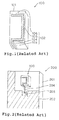
- Figs. 1 and 2 the antenna element disclosed in the above-cited application will be described below in brief, as a related art which precedes the present invention and is not known.
- the antenna element described below was filed in Japan on February 1, 2001 as Japanese Patent Application No. 2001-026002, and filed in the United States of America on January 31, 2002 as USSN 10/059423 by the present inventor.
- this application has not been opened in any country, so that this is not a prior art but merely a related art of the present invention.
- Antenna element 100 in the aforementioned application has device substrate 101 made of a dielectric material, and conductive line 102 formed of a printed wire on a front surface and a bottom surface of device substrate 101.
- Conductive line 102 is comprised of power supply conductor 103, first conductor 104, short-circuit conductor 105, and second conductor 106, each of which is linearly formed in succession.
- power supply conductor 103 of conductive line 102 comprises a linear portion formed from the bottom surface to the front surface of device substrate 101, while first conductor 104 comprises a linear portion formed from an upper end which is a terminate end of power supply conductor 103 and bent at a right angle to the right in the figure.
- Short-circuit conductor 105 comprises a linear portion formed from a right end which is a terminate end of first conductor 104 and bent upward at a right angle in the figure, i.e., in the opposite direction to power supply conductor 103, while second conductor 106 comprises a linear portion formed from an upper end which is a terminate end of short-circuit conductor 105 and bent at a right angle to the left in the figure, and positioned in parallel to first conductor 104.
- antenna apparatus 200 using antenna element 100 as described above comprises a circuit board 201 made of glass epoxy resin, ethylene tetrafluoride or the like, as illustrated in Fig. 2.
- a copper foil is adhered in a lower half and the like of a front surface of circuit board 201 to form a ground electrode 202.
- Ground electrode 202 is partially formed with a recess in which power supply electrode 204 is formed for power supply circuit 203 (for example, a coaxial cable) which serves as a power supply means. Then, antenna element 100 is mounted on an upper half of the front surface of circuit board 201 on which ground electrode 202 is not formed. Power supply conductor 103 is connected to power supply electrode 204.
- power supply circuit 203 for example, a coaxial cable
- conductive line 102 can be reduced in length since first conductor 104 and second conductor 106, positioned in parallel to each other, act as a loaded inductance. In addition, since conductive line 102 is generally bent in an inverted C-shape, the overall shape can be reduced in size.
- first conductor 104 and second conductor 106 are sufficiently spaced away from each other, so that their electromagnetic coupling is reduced, thereby making it possible to realize radio communications with a high gain, high efficiency and wide band.
- short-circuit conductor 105 mainly transmits and receives radio waves
- the transmission/reception have a directivity in the horizontal direction in the figure orthogonal to the longitudinal direction of the short-circuit conductor 105. For this reason, if a conductor such as ground electrode 202 is positioned in a direction orthogonal to short-circuit conductor 105, the conductor will impede the transmission/reception of radio waves through short-circuit conductor 105.
- ground electrode 202 In the foregoing problem, it is contemplated to avoid forming ground electrode 202 and the like in the direction orthogonal to short-circuit conductor 105. However, this solution would cause a reduction in the area of ground electrode 202 available for mounting circuit parts (not shown). In other words, it is necessary to minimize an antenna mounting area on which ground electrode 202 is not formed in order to maximize an area available for mounting circuit parts.
- an antenna element of the present invention includes a device substrate and a conductive line which is comprised of at least a power supply conductor, a first conductor, a short-circuit conductor, and a second conductor.
- the device substrate is made of at least one of a dielectric material and a magnetic material, and is formed with the power supply conductor, first conductor, short-circuit conductor, and second conductor.
- the power supply conductor is made of a linear conductor, and supplied with electric power at a leading end thereof.
- the first conductor is connected to a terminate end of the power supply conductor at a right angle, while the short-circuit conductor is connected to a terminate end of the first conductor at a right angle on the opposite side of the power supply conductor.
- the second conductor is connected to a terminate end of the short-circuit conductor at a right angle, and positioned in parallel to the first conductor.
- the device substrate is also formed with a ground conductor which has a terminate end connected to the conductive line, and a leading end applied with a ground potential.
- the antenna element can have an increased radiation resistance. Also, impedance matching can be adjusted by changing reactance and/or resistance of input impedance of the conductive line.
- the resonance frequency can also be adjusted by a position at which the ground conductor is connected to the conductive line. Further, the performance can be improved in the antenna element which includes a loaded inductance formed of the parallel first and second conductors.
- a capacitive conductor having a given capacitance is formed as part of the conductive line, and connected to a terminate end of the second conductor.
- the conductive line can be reduced in length by a loaded capacitance of the capacitive conductor, so that the antenna element can be reduced in size.
- the ground conductor has a terminate end electromagnetically coupled to the conductive line in non-contact manner. Since the electromagnetic coupling eliminates the need for directly connecting the ground conductor to the conductive line, the ground conductor can be readily formed.
- a first antenna apparatus includes an antenna element, a circuit board, a ground electrode, and a ground wire.
- the antenna element includes the antenna element according to the present invention, and the circuit board has the antenna element mounted on a front surface thereof.
- the ground electrode is formed at a position spaced apart from the antenna element on the front surface of the circuit board for generating a ground potential.
- the ground wire is formed on the front surface of the circuit board, and has a leading end connected to the ground electrode, and a terminate end connected to a leading end of the ground conductor.
- a second antenna apparatus includes a device substrate, a conductor line, a circuit board, a ground electrode, and a ground wire.
- the conductive line is comprised of a power supply conductor, a first conductor, a short-circuit conductor, and a second conductor.
- the device substrate is made of at least one of a dielectric material and a magnetic material, and is formed with the power supply conductor, first conductor, short-circuit conductor, and second conductor.
- the power supply conductor is made of a linear conductor, and is supplied with electric power with a leading end thereof.
- the first conductor is connected at a right angle to a terminate end of the power supply conductor, while the short-circuit conductor is connected at a right angle to a terminate end of the first conductor on the opposite side of the power supply conductor.
- the second conductor is connected at a right angle to a terminate end of the short-circuit conductor, and positioned in parallel to the first conductor.
- the circuit board is mounted with the device substrate on a front surface thereof.
- the ground electrode is formed at a position spaced apart from the device substrate on the front surface of the circuit board for generating a ground potential.
- the ground wire is formed on the front surface of the circuit board, and has a leading end connected to the ground electrode, and a terminate end connected to a leading end of the ground conductor.
- the ground conductor of the antenna element can function in a manner similar to a conventional short pin.
- a capacitive conductor having a given capacitance is connected to a terminate end of the second conductor and additionally formed as part of the conductive line.
- the conductive line can be reduced in length by a loaded capacitance of the capacitive conductor, making it possible to reduce the antenna apparatus as well as the antenna element in size.
- the ground conductor since the ground conductor has a terminate end electromagnetically coupled to the conductive line in non-contact manner, the ground conductor need not be directly connected to the conductive line. Consequently, the ground conductor, for example, may be formed only on the front surface of he circuit board without extending to the antenna element, thereby facilitating the formation of the ground conductor.
- a third antenna apparatus includes a conductive line, a device substrate, a circuit board, a ground electrode, a power supply electrode, and a ground wire.
- the device substrate is made of at least one of a dielectric material and a magnetic material, and is formed with the conductive line.
- the circuit board is mounted with the device substrate on a front surface thereof.
- the ground electrode is formed at a position spaced apart from the device substrate on a front surface of the circuit board for generating a ground potential.
- the power supply electrode has a terminate end connected to the conductive line on the device substrate, and is supplied with electric power at a leading end.
- the ground wire which is formed on the front surface of the circuit board, has a leading end connected to the ground electrode, and a terminate end connected to the power supply electrode.
- the ground wire functions in a manner similar to a conventional short pin.
- the present invention can provide a reduction in the entire size of the antenna apparatus, as well as a wider bandwidth and a higher efficiency for the same.
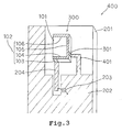
- antenna element 300 in this embodiment comprises device substrate 101 made of a dielectric material, and conductive line 102 on front and bottom surfaces of device substrate 101.
- Conductive line 102 is comprised of a power supply conductor 103, first conductor 104, short-circuit conductor 105, and second conductor 106.
- antenna apparatus 400 in this embodiment has ground electrode 202 in a lower half and the like of a front surface of circuit board 201, and power supply electrode 204 of power supply circuit 203, serving as a power supply means, formed in a recess of ground electrode 202.
- Antenna element 300 is mounted in an upper half of the front surface of circuit board 201 on which ground electrode 202 is not formed. Power supply conductor 103 of antenna element 300 is connected to power supply electrode 204.
- antenna element 300 in this embodiment additionally has ground conductor 301 formed on a side surface of device substrate 101.
- Ground conductor 301 is connected to conductive line 102.
- ground conductor 301 has a terminate end connected near a leading end of short-circuit conductor 105, and a leading end positioned on the boundary of a side surface and a rear surface of device substrate 101.
- antenna apparatus 400 in this embodiment has ground wire 401 on the front surface of circuit board 201.
- Ground wire 401 has a leading end connected to ground electrode 202.
- ground wire 401 has a terminate end connected to a leading end of ground conductor 301 of antenna element 300, a ground potential at ground electrode 202 is applied to ground conductor 301 of antenna element 300 through ground wire 401.
- antenna element 300 in this embodiment is similar to the aforementioned antenna element 100 in that first conductor 104 and second conductor 106 positioned in parallel to each other act as a loaded inductance, so that the length of conductive line 102 is reduced to make the overall shape smaller, while ensuring a desired resonant frequency.
- first conductor 104 and second conductor 106 positioned in parallel to each other are sufficiently spaced apart from each other, so that their electromagnetic coupling is reduced, making it possible to realize radio communications with a high gain, high efficiency, and wide band.
- ground conductor 301 is connected at a predetermined position of conductive line 102 of antenna element 300, so that ground conductor 301 is applied with the ground potential at ground electrode 202 through ground wire 401.
- ground conductor 301 can function as a conventional short pin to increase a radiation resistance of antenna element 300, so that impedance matching can be adjusted by changing reactance and/or resistance of input impedance of conductive line 102.
- antenna element 300 since improved performance can be achieved for antenna element 300 which uses parallel first conductor 104 and second conductor 106 as a loaded inductance, antenna element 300 can transmit and receive radio waves relatively satisfactorily even if a conductor such as ground electrode 202 is positioned in a direction orthogonal to short-circuit conductor 105.
- antenna apparatus 400 can be reduced in size without the need for reducing ground electrode 202 in a downward or a lateral direction in the figure.
- conductive line 102 is comprised of power supply conductor 103, first conductor 104, short-circuit conductor 105 and second conductor 106.
- capacitive conductors 507 - 509 having given capacitances may be added as parts of conductive lines 504 - 506.
- connection conductor 510 formed on the top surface of device substrate 101 may have a leading end connected to a terminate end of second conductor 106 on the front surface, and capacitive conductor 507 likewise formed on the top surface of device substrate 101 may be connected to a terminate end of connection conductor 510.
- capacitive conductor 508 formed over the entire top surface of device substrate 101 may be connected directly to second conductor 106.
- capacitive conductor 509 formed over the entire top surface of device substrate 101 may be used as second conductor 106.
- capacitances of capacitive conductors 507 - 509 as mentioned above are generated between capacitive conductors 507 - 509 and ground electrode 202, so that the capacitances of capacitive conductors 507 - 509 vary depending on their sizes and shapes, relationships with ground electrode 202 in distance and shape, and the like.
- the capacitances are adjusted corresponding to the resonant frequencies of conductive lines 504 - 506 by a computer simulation or the like.
- antenna elements 501 - 503 as described above provide a reduction in resonant frequency by virtue of loaded capacitances of capacitive conductors 507 - 509, antenna elements 501 - 503 can be reduced in overall shape, with reduced conductive lines 504 - 506, without relatively increasing the resonant frequency.
- illustrative antenna apparatus 400 in the foregoing embodiment adjusts impedance matching by changing reactance and resistance of input impedance of conductive line 102, ground conductor 301 of antenna element 300, to which ground wire 401 is connected, is connected near a leading end of short-circuit conductor 105.
- ground conductor 603 of antenna element 602, to which ground conductor 601 is connected may be connected to first conductor 104.
- ground conductor 702 of antenna element 701 may be connected near a terminate end of short-circuit conductor 105.
- antenna apparatus 600, 700 as described above has a pass of current defined by a path extending from a leading end of power supply electrode 204 to a terminate end of conductive line 102 and turning back to a leading end of ground wire 601, 401, the resonant frequency can be adjusted by changing the position of conductive line 102 at which ground conductor 603, 702 is connected, and the lengths of ground wire/conductor 601, 603, 401, 702.
- antenna apparatus 400 in the foregoing embodiment illustrates ground conductor 301 of antenna element 300 directly connected to conductive line 102
- ground conductor 802 of antenna element 801 may be electromagnetically coupled to conductive line 102 in non-contact manner, as antenna apparatus 800 illustrated in Fig. 7.
- antenna apparatus 400 in the foregoing embodiment illustrates that ground conductor 301 connected to conductive line 102 is also formed in antenna element 300, ground wire 901 formed only on the front surface of circuit board 201 may be connected to conductive line 504 of antenna element 902, as antenna apparatus 900 illustrated in Fig. 8.
- this antenna apparatus 900 has capacitive conductor 507 formed on the top surface of antenna element 902, ground wire 901 is readily connected to capacitive conductor 507.
- ground wire 901 is connected to a terminate end of conductive line 504 in this manner, conductive line 504 and ground wire 901 can function as a folded antenna.
- Connection 903 is formed integrally with terminate ends of power supply electrode 204 and ground wire 901, and connection 904 in the same shape is also formed integrally with power supply conductor 103 and capacitive conductor 507 on a back surface of antenna element 902.
- connections 903, 904 are connected by soldering to electrically connect power supply conductor 103 to power supply electrode 204, electrically connect capacitive conductor 507 to ground wire 901, and secure antenna element 902 integrally with circuit board 201.
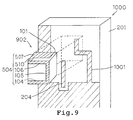
- ground wire 1001 formed only on the front surface of circuit board 201 may be electromagnetically coupled to conductive line 504 of antenna element 902 in non-contact manner.
- antenna apparatus 1000 can be readily manufactured because ground wire 1001 formed on circuit board 201 need not be directly connected to conductive line 504 formed on device substrate 101.
- power supply conductor 103 is not illustrated in Figs. 8 and 9, it is actually formed on the bottom surface of device substrate 101 and connected to power supply electrode 204, as is the case with Fig. 3 and other figures.
- ground wire 1101 formed on the surface of circuit board 201 may be connected to power supply electrode 204 formed on the surface of circuit board 201, as antenna apparatus 1100 illustrated in Fig. 10.
- such antenna apparatus 1100 readily provides a reduction in resonant frequency, an increase in bandwidth and radiation efficiency, and the like by forming longer ground wire 1101, and defining a position at which ground wire 1101 is connected in close proximity to a leading end of power supply electrode 204.
- ground wire 1101 longer than power supply electrode 204 results in an increased antenna length and resulting reduction in resonant frequency, as described above, the whole apparatus can be relatively reduced in size.
- antenna apparatus 1100 has a lower resonant frequency in this manner, conductive line 102 may be made wider to increase the bandwidth.
- antenna apparatus 1100 can be simplified in structure.
- ground wire 1101 is connected to power supply electrode 204 on the surface of circuit board 201 may be applied to a conventional dielectric antenna which does not comprise parallel first conductor 104 and second conductor 106.
- ground conductor 301 and ground wire 401 are provided in antenna element 300 and the like in the foregoing illustrative embodiment, a plurality of these elements may be provided. Since antenna element 300 functions similarly to a folded antenna by the action of ground conductor 301 and ground wire 401, an increase in the number of ground conductor 301 and ground wire 401 can result in an increased radiation resistance and an improved radiation efficiency. Alternatively, the radiation resistance can be increased to improve the radiation efficiency by increasing line widths of ground conductor 301 and ground wire 401.
Landscapes
- Engineering & Computer Science (AREA)
- Computer Networks & Wireless Communication (AREA)
- Details Of Aerials (AREA)
- Waveguide Aerials (AREA)
- Support Of Aerials (AREA)
Applications Claiming Priority (2)
| Application Number | Priority Date | Filing Date | Title |
|---|---|---|---|
| JP2001181815 | 2001-06-15 | ||
| JP2001181815A JP2002374115A (ja) | 2001-06-15 | 2001-06-15 | アンテナ素子、アンテナ装置、無線通信装置 |
Publications (2)
| Publication Number | Publication Date |
|---|---|
| EP1267440A2 true EP1267440A2 (de) | 2002-12-18 |
| EP1267440A3 EP1267440A3 (de) | 2004-04-21 |
Family
ID=19022022
Family Applications (1)
| Application Number | Title | Priority Date | Filing Date |
|---|---|---|---|
| EP02009597A Withdrawn EP1267440A3 (de) | 2001-06-15 | 2002-04-26 | Antennenelement mit auf äusseren Oberflächen eines Substratkörpers geformten Leitern |
Country Status (5)
| Country | Link |
|---|---|
| US (1) | US6700543B2 (de) |
| EP (1) | EP1267440A3 (de) |
| JP (1) | JP2002374115A (de) |
| CN (1) | CN1237658C (de) |
| TW (1) | TW538558B (de) |
Cited By (3)
| Publication number | Priority date | Publication date | Assignee | Title |
|---|---|---|---|---|
| WO2008065241A1 (en) | 2006-11-28 | 2008-06-05 | Pulse Finland Oy | Dielectric antenna |
| EP2493011A1 (de) * | 2011-02-25 | 2012-08-29 | Acer Incorporated | Mobiles Kommunikationsgerät und Antennenstruktur dafür |
| US10879619B2 (en) | 2009-06-04 | 2020-12-29 | Ubiquiti Inc. | Microwave system |
Families Citing this family (26)
| Publication number | Priority date | Publication date | Assignee | Title |
|---|---|---|---|---|
| US20040021606A1 (en) * | 2002-07-11 | 2004-02-05 | Alps Electric Co., Ltd. | Small plane antenna and composite antenna using the same |
| JP3825400B2 (ja) * | 2002-12-13 | 2006-09-27 | 京セラ株式会社 | アンテナ装置 |
| JP2004266311A (ja) * | 2003-01-15 | 2004-09-24 | Fdk Corp | アンテナ |
| JP2005051747A (ja) * | 2003-07-14 | 2005-02-24 | Ngk Spark Plug Co Ltd | アンテナ装置およびその製造方法 |
| JP4232026B2 (ja) | 2004-02-27 | 2009-03-04 | ミツミ電機株式会社 | 複合アンテナ装置及びそれを備えた移動体 |
| JP2006314005A (ja) * | 2005-05-09 | 2006-11-16 | Nippon Antenna Co Ltd | 内蔵アンテナ |
| CN101171721B (zh) * | 2005-05-11 | 2013-01-23 | 株式会社村田制作所 | 天线结构及包含该天线结构的无线通信装置 |
| JP4999349B2 (ja) * | 2006-04-05 | 2012-08-15 | 株式会社ソニー・コンピュータエンタテインメント | アンテナおよびそれを利用した無線通信装置 |
| TWI319641B (en) * | 2006-04-20 | 2010-01-11 | Chant Sincere Co Ltd | Chip antenna apparatus for receiving global positioning system signals |
| EP2104178A4 (de) * | 2007-01-19 | 2014-05-28 | Murata Manufacturing Co | Antenneneinheit und drahtlose kommunikationsvorrichtung |
| DE112008000578B4 (de) * | 2007-03-23 | 2014-05-22 | Murata Mfg. Co., Ltd. | Antenne und Funkkommunikationsvorrichtung |
| JP4867753B2 (ja) * | 2007-03-30 | 2012-02-01 | Tdk株式会社 | アンテナ装置及びこれを用いた無線通信機器 |
| US20080309558A1 (en) * | 2007-06-14 | 2008-12-18 | Yu Yao-Wen | Micro antenna structure |
| JP4941202B2 (ja) * | 2007-09-26 | 2012-05-30 | Tdk株式会社 | アンテナ装置及びその特性調整方法 |
| JP4124802B1 (ja) * | 2007-10-30 | 2008-07-23 | 松下電器産業株式会社 | 携帯無線装置 |
| JP4707728B2 (ja) * | 2008-03-28 | 2011-06-22 | パナソニック株式会社 | 携帯無線装置 |
| KR101007904B1 (ko) * | 2008-08-11 | 2011-01-14 | 주식회사 에이스테크놀로지 | 케이블들을 전기적으로 연결시키는 안테나 |
| TWI383539B (zh) * | 2009-08-14 | 2013-01-21 | Univ Nat Chiao Tung | 共平面天線單元及共平面天線 |
| JP5035323B2 (ja) * | 2009-11-06 | 2012-09-26 | 株式会社村田製作所 | アンテナ |
| CN102683830A (zh) * | 2011-03-11 | 2012-09-19 | 宏碁股份有限公司 | 移动通信装置及其天线结构 |
| CN102856635B (zh) * | 2011-06-27 | 2016-05-04 | 光宝电子(广州)有限公司 | 多频天线及具有该多频天线的电子装置 |
| WO2013161388A1 (ja) * | 2012-04-25 | 2013-10-31 | 株式会社村田製作所 | 無線icデバイス及び無線通信端末 |
| KR101360561B1 (ko) * | 2012-06-28 | 2014-02-11 | 엘지이노텍 주식회사 | 안테나 장치 |
| TWI509892B (zh) * | 2013-03-21 | 2015-11-21 | Arcadyan Technology Corp | 天線結構及其製造方法 |
| JP5726983B2 (ja) * | 2013-10-30 | 2015-06-03 | 太陽誘電株式会社 | チップ状アンテナ装置及び送受信用通信回路基板 |
| KR102408139B1 (ko) * | 2017-08-25 | 2022-06-15 | 삼성전자주식회사 | 안테나 장치 및 그를 포함하는 전자 장치 |
Family Cites Families (10)
| Publication number | Priority date | Publication date | Assignee | Title |
|---|---|---|---|---|
| US5696517A (en) * | 1995-09-28 | 1997-12-09 | Murata Manufacturing Co., Ltd. | Surface mounting antenna and communication apparatus using the same |
| JP3114582B2 (ja) * | 1995-09-29 | 2000-12-04 | 株式会社村田製作所 | 表面実装型アンテナおよびこれを用いた通信機 |
| US5748149A (en) * | 1995-10-04 | 1998-05-05 | Murata Manufacturing Co., Ltd. | Surface mounting antenna and antenna apparatus |
| JP3114621B2 (ja) * | 1996-06-19 | 2000-12-04 | 株式会社村田製作所 | 表面実装型アンテナおよびこれを用いた通信機 |
| JP3279205B2 (ja) * | 1996-12-10 | 2002-04-30 | 株式会社村田製作所 | 表面実装型アンテナおよび通信機 |
| JPH1127025A (ja) * | 1997-07-03 | 1999-01-29 | Murata Mfg Co Ltd | アンテナ装置 |
| JP3663888B2 (ja) * | 1998-03-02 | 2005-06-22 | 株式会社村田製作所 | 表面実装型アンテナおよびそれを搭載した通信機 |
| JP3246440B2 (ja) * | 1998-04-28 | 2002-01-15 | 株式会社村田製作所 | アンテナ装置およびそれを用いた通信機 |
| JP3661432B2 (ja) * | 1998-08-24 | 2005-06-15 | 株式会社村田製作所 | 表面実装型アンテナおよびそれを用いたアンテナ装置およびそれを用いた通信機 |
| JP2002299933A (ja) * | 2001-04-02 | 2002-10-11 | Murata Mfg Co Ltd | アンテナの電極構造およびそれを備えた通信機 |
-
2001
- 2001-06-15 JP JP2001181815A patent/JP2002374115A/ja active Pending
-
2002
- 2002-04-25 US US10/131,462 patent/US6700543B2/en not_active Expired - Fee Related
- 2002-04-26 TW TW091108743A patent/TW538558B/zh not_active IP Right Cessation
- 2002-04-26 EP EP02009597A patent/EP1267440A3/de not_active Withdrawn
- 2002-06-04 CN CNB021222851A patent/CN1237658C/zh not_active Expired - Fee Related
Cited By (5)
| Publication number | Priority date | Publication date | Assignee | Title |
|---|---|---|---|---|
| WO2008065241A1 (en) | 2006-11-28 | 2008-06-05 | Pulse Finland Oy | Dielectric antenna |
| EP2097946A4 (de) * | 2006-11-28 | 2009-11-18 | Pulse Finland Oy | Dielektrische antenne |
| US10879619B2 (en) | 2009-06-04 | 2020-12-29 | Ubiquiti Inc. | Microwave system |
| EP2493011A1 (de) * | 2011-02-25 | 2012-08-29 | Acer Incorporated | Mobiles Kommunikationsgerät und Antennenstruktur dafür |
| US8836582B2 (en) | 2011-02-25 | 2014-09-16 | Acer Incorporated | Mobile communication device and antenna structure therein |
Also Published As
| Publication number | Publication date |
|---|---|
| EP1267440A3 (de) | 2004-04-21 |
| JP2002374115A (ja) | 2002-12-26 |
| US20020190907A1 (en) | 2002-12-19 |
| TW538558B (en) | 2003-06-21 |
| US6700543B2 (en) | 2004-03-02 |
| CN1392632A (zh) | 2003-01-22 |
| CN1237658C (zh) | 2006-01-18 |
Similar Documents
| Publication | Publication Date | Title |
|---|---|---|
| US6700543B2 (en) | Antenna element with conductors formed on outer surfaces of device substrate | |
| JP7028954B2 (ja) | アンテナ及び移動端末 | |
| US7760150B2 (en) | Antenna assembly and wireless unit employing it | |
| US6204826B1 (en) | Flat dual frequency band antennas for wireless communicators | |
| JP4823433B2 (ja) | 移動電話のための統合アンテナ | |
| CN100388560C (zh) | 用于移动装置的带宽加宽天线 | |
| US6700541B2 (en) | Antenna element with conductors formed on outer surfaces of device substrate | |
| EP1182727A2 (de) | Antennenanordnung und tragbares drahtloses Kommunikationsgerät | |
| US20050035919A1 (en) | Multi-band printed dipole antenna | |
| US7050009B2 (en) | Internal antenna | |
| KR20020044585A (ko) | 평형 인입식 이동전화 안테나 | |
| US7170456B2 (en) | Dielectric chip antenna structure | |
| US7205944B2 (en) | Methods and apparatus for implementation of an antenna for a wireless communication device | |
| US6172646B1 (en) | Antenna apparatus and communication apparatus using the antenna apparatus | |
| JP2004506363A (ja) | ワイヤレス端末 | |
| WO2000052783A1 (en) | Broadband antenna assembly of matching circuitry and ground plane conductive radiating element | |
| JP2002290138A (ja) | アンテナ装置 | |
| JPH11340726A (ja) | アンテナ装置 | |
| WO2025256431A1 (zh) | 一种电子设备 | |
| WO2025201318A1 (zh) | 一种电子设备 | |
| JP2002319809A (ja) | アンテナ装置 | |
| JP7407487B1 (ja) | 伝送装置及びアンテナ | |
| KR100861865B1 (ko) | 무선 단말기 | |
| US5920293A (en) | Radio frequency (RF) antenna coupler with an electrically extended ground plane | |
| KR100413010B1 (ko) | 소형 유전체 안테나 |
Legal Events
| Date | Code | Title | Description |
|---|---|---|---|
| PUAI | Public reference made under article 153(3) epc to a published international application that has entered the european phase |
Free format text: ORIGINAL CODE: 0009012 |
|
| AK | Designated contracting states |
Kind code of ref document: A2 Designated state(s): AT BE CH CY DE DK ES FI FR GB GR IE IT LI LU MC NL PT SE TR |
|
| AX | Request for extension of the european patent |
Free format text: AL;LT;LV;MK;RO;SI |
|
| RAP1 | Party data changed (applicant data changed or rights of an application transferred) |
Owner name: NEC TOKIN CORPORATION Owner name: NEC MICROWAVE TUBE, LTD. |
|
| PUAL | Search report despatched |
Free format text: ORIGINAL CODE: 0009013 |
|
| AK | Designated contracting states |
Kind code of ref document: A3 Designated state(s): AT BE CH CY DE DK ES FI FR GB GR IE IT LI LU MC NL PT SE TR |
|
| AX | Request for extension of the european patent |
Extension state: AL LT LV MK RO SI |
|
| 17P | Request for examination filed |
Effective date: 20040306 |
|
| 17Q | First examination report despatched |
Effective date: 20040624 |
|
| AKX | Designation fees paid |
Designated state(s): DE FR GB |
|
| STAA | Information on the status of an ep patent application or granted ep patent |
Free format text: STATUS: THE APPLICATION IS DEEMED TO BE WITHDRAWN |
|
| 18D | Application deemed to be withdrawn |
Effective date: 20050105 |