EP1271738B1 - Déclencheur électronique comportant un condensateur d'alimentation d'une bobine de déclenchement - Google Patents
Déclencheur électronique comportant un condensateur d'alimentation d'une bobine de déclenchement Download PDFInfo
- Publication number
- EP1271738B1 EP1271738B1 EP02354049A EP02354049A EP1271738B1 EP 1271738 B1 EP1271738 B1 EP 1271738B1 EP 02354049 A EP02354049 A EP 02354049A EP 02354049 A EP02354049 A EP 02354049A EP 1271738 B1 EP1271738 B1 EP 1271738B1
- Authority
- EP
- European Patent Office
- Prior art keywords
- capacitor
- voltage
- trip device
- circuit
- supply
- Prior art date
- Legal status (The legal status is an assumption and is not a legal conclusion. Google has not performed a legal analysis and makes no representation as to the accuracy of the status listed.)
- Expired - Lifetime
Links
Images



Classifications
-
- H—ELECTRICITY
- H02—GENERATION; CONVERSION OR DISTRIBUTION OF ELECTRIC POWER
- H02H—EMERGENCY PROTECTIVE CIRCUIT ARRANGEMENTS
- H02H1/00—Details of emergency protective circuit arrangements
- H02H1/06—Arrangements for supplying operative power
- H02H1/063—Arrangements for supplying operative power primary power being supplied by fault current
- H02H1/066—Arrangements for supplying operative power primary power being supplied by fault current and comprising a shunt regulator
Definitions
- the invention relates to an electronic trip device comprising means for measurement of the current connected to an electronic processing circuit, intended for perform protection functions and compare the measured current to at least one trip threshold, and to a supply circuit comprising a capacitor supply and voltage regulation means across the capacitor as a function of a predetermined reference voltage.
- the trigger coil is generally supplied by a supply capacitor of a supply circuit.
- the supply capacitor is charged by current sensors associated with the conductors of an electrical network to be protected.
- the supply circuit is generally of the switching supply type, for regulating the voltage across the supply capacitor.
- the document US-A-4,567,540 describes a supply circuit comprising a supply capacitor and voltage regulation means at the terminals of the capacitor as a function of a reference voltage, for a trip unit electronic device comprising current measurement means connected to a circuit processing electronics and intended to provide protection functions.
- a first supply voltage of the order of 18V is generally necessary at the terminals of the supply capacitor for ensure reliable tripping by the tripping coil.
- the lifetime of a capacitor being determined by the difference between the voltage maximum acceptable by the capacitor (nominal capacitor voltage) and the actual operating voltage, the reliability of the trigger capacitor implies the use of capacitors of sufficient size.
- the object of the invention is a trigger making it possible to maintain or increase the reliability of the trigger capacitor, while reducing the size and cost of this one.
- the electronic circuit of processing includes means for comparing the current measured to a threshold predetermined, below the triggering threshold, the trigger comprising means for fixing the reference voltage of the regulating means to a first predetermined value during a predetermined period, during a energizing the release or when the measured current is equal or greater than the predetermined threshold, and a second predetermined value, less than the first, after said predetermined period.
- the second value of the voltage reference is less than the voltage required to activate a coil trigger release.
- FIG. 1 An electronic trigger according to the prior art is illustrated in FIG. 1. Only the elements necessary for understanding the invention have been shown in the figure.
- the trigger signal D is applied to a control electrode of an electronic switch 3, for example constituted by a thyristor.
- the closing of the electronic switch 3 by a trigger signal D causes the excitation of a trigger coil 4, connected in series with the electronic switch at the terminals of a first supply voltage V 1 .
- the first supply voltage V 1 is supplied by a supply circuit 5.
- the supply circuit 5 is supplied by current sensors associated with the conductors of the electrical network to be protected.
- the current sensors connected to the supply circuit can be the current sensors 1 or, as shown in FIG. 1, current sensors 6 distinct from the previous ones.
- the current sensors 1 are preferably air sensors, for example constituted by Rogowski toroids, while the current sensors 6 are preferably sensors with an iron core.
- the supply circuit 5 also supplies a second supply voltage V 2 , lower than the first, sufficient for supplying the various electronic circuits of the trip device.
- the supply circuit 5 is of the switching supply type, making it possible to regulate the voltage across the terminals of the supply capacitor.
- the current sensors, 1 or 6 are connected to a rectification circuit 7, preferably of the full-wave rectifier type, comprising two output terminals, one of which is connected to ground and the other to a conductor 8.
- An electronic switch 9, acting as a chopper, is connected in parallel to the output terminals of the rectification circuit.
- a first output terminal of the supply circuit 5, supplying the first supply voltage V 1 is connected to the conductor 8 via a diode 10, connected so as to be conductive when the voltage at the output of the rectifier circuit 7 is greater than V 1 and blocked in the opposite case.
- a capacitor C is connected, in parallel with a voltage divider, between the first output terminal of the supply circuit 5 and the ground.
- the voltage divider is a resistive divider constituted by first and second resistors R 1 and R 2 connected in series. The midpoint of the resistive divider is connected to an input of a regulation circuit 11, which controls the electronic switch 9.
- a third resistor R 3 is connected, in series with a Zener diode Zd, in parallel on the capacitor C, the point common to the third resistor R 3 and the Zener diode Zd constituting a second output terminal of the supply circuit 5, supplying the second supply voltage V 2 .
- the voltage V 3 at the midpoint of the resistive divider is representative of the voltage V 1 at the terminals of the capacitor.
- the regulation circuit 11 keeps the electronic switch 9 in the open position (blocking in the case of a transistor).
- the conductor C is therefore charged, via the rectifying circuit 7 and the diode 10, from the current transformers.
- the regulation circuit 11 closes the electronic switch 9 (conduction in the case of a transistor), thus short-circuiting the output of the rectification circuit.
- the diode 10 then blocks, preventing the charging of the capacitor C.
- the first supply voltage V 1 is thus regulated to the value of the predetermined reference voltage.
- the second supply voltage V 2 is then obtained at the terminals of the Zener diode Zd.
- the reference voltage is chosen so that ensure the triggering of the trip coil at all times default. For example, if the voltage required for a trip reliable of the release coil 4 is around 18V, the voltage of reference is fixed at a value of 19V.
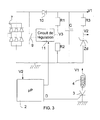
- the trigger according to the invention shown in Figure 3 differs from that described above by the fact that the regulation circuit 11 has an input additional connected to an additional output of the electronic circuit of treatment 2 of the trigger.
- the electronic processing circuit 2 causes a modification of the reference voltage of the regulation circuit 11 so that that it takes a first predetermined value for a period predetermined, when the trigger is energized or when the current measured I is equal to or greater than a predetermined threshold Is, less than the threshold of trigger, and at a second predetermined value, lower than the first, after said predetermined period.
- the voltage V 1 across the capacitor C is zero. With the electronic switch 9 open, the capacitor begins to charge. The voltage V 1 increases. At an instant t 1 , it reaches a sufficient value, for example 8V in FIG. 4A, to supply the electronic circuits of the trip device and more particularly the electronic processing circuit 2.
- a supply signal A (FIG. 4b), up to here at 0, then takes the value 1, initializing a start-up phase F1 (FIG. 5) of the microprocessor of the electronic processing circuit. This then sets to zero, in a phase F2, a quantity ⁇ t, then fixes, in a phase F3, the value of the reference voltage Vref to a first value. In the particular embodiment shown, this first value of the reference voltage is 19V. Under the control of the electronic processing circuit 2, the regulation circuit 11 uses this first value of the reference voltage for a predetermined period T, for example between 10 milliseconds and 100 milliseconds.
- step F7 the microprocessor monitors (step F7) whether a predetermined threshold Is, lower than the triggering threshold, by the measured current I (I ⁇ Is?). As long as the measured current remains below this threshold (No output of F7), the reference voltage remains unchanged and the microprocessor continues its monitoring of the evolution of the current by closing on step F7.
- the microprocessor loops on step F2.
- the reference voltage Vref then takes the first value, the highest, and the capacitor C recharges until reaching this value.
- the exceeding of the threshold Is by the current indicates that the latter has exceeded its normal value and constitutes an indication of the possibility of the imminence of the detection of a fault which should lead to a trip.
- the threshold Is can be equal to 2 In. If, during the period T, following time t 3 , the electronic processing circuit 2 does not detect a fault, the reference voltage returns to its second value after this period.
- a trigger signal D is then emitted, at time t 4 in FIG. 4b.
- the supply circuit 5 is then no longer supplied by the current sensors and the capacitor C discharges.
- the microprocessor takes measures to save certain data during the period t 4 -t 5 following the triggering.
- the specific values (19V and 10V) of the reference voltage are fixed during steps F3 and F5, these values being then transmitted to the regulation circuit 11.
- the two values which can be taken by the reference voltage Vref are predetermined within the control circuit and the microprocessor does not transmits to the control circuit that a binary signal representative of the value at use.
- the invention thus makes it possible to reduce the size, and therefore the cost, of the capacitor C supply of the trip coil 4, while ensuring a reliable operation of the latter in the event of a fault.
- a trigger being a relatively rare event, the capacitor is only fully charged during short periods, for example 1s, during which a fault is likely to occur, in this case when the trigger is energized and when the measured current reaches a predetermined threshold Is.
- a 22 ⁇ F capacitor with a maximum voltage of 35V can be replaced by a 22 ⁇ F capacitor with a maximum voltage of 25V.
- the invention is not limited to the particular embodiments described above. In particular, it is not limited to a switching power supply of the step-down type but also applies, analogously, in the case of a switching power supply of the step-up type.
Landscapes
- Engineering & Computer Science (AREA)
- Power Engineering (AREA)
- Emergency Protection Circuit Devices (AREA)
Description
Claims (5)
- Déclencheur électronique comportant des moyens (1, 6) de mesure du courant connectés à un circuit électronique de traitement (2), destiné à réaliser des fonctions de protection et comparant le courant mesuré à au moins un seuil de déclenchement, et à un circuit d'alimentation (5) comportant un condensateur d'alimentation (C) et des moyens (11) de régulation de la tension aux bornes du condensateur en fonction d'une tension de référence (Vref) prédéterminée, déclencheur caractérisé en ce que le circuit électronique de traitement (2) comporte des moyens de comparaison du courant mesuré (I) à un seuil prédéterminé (Is), inférieur au seuil de déclenchement, le déclencheur comportant des moyens pour fixer la tension de référence (Vref) des moyens (11) de régulation à une première valeur prédéterminée pendant une période prédéterminée (T), lors d'une mise sous tension du déclencheur ou lorsque le courant mesuré (I) est égal ou supérieur au seuil prédéterminé (Is), et à une seconde valeur prédéterminée, inférieure à la première, après ladite période prédéterminée.
- Déclencheur selon la revendication 1, caractérisé en ce que la seconde valeur de la tension de référence (Vref) est inférieure à la tension nécessaire pour activer une bobine de déclenchement (4) du déclencheur.
- Déclencheur selon l'une des revendications 1 et 2, caractérisé en ce que le circuit de régulation (11) comporte une entrée connectée à une sortie du circuit électronique de traitement (2).
- Déclencheur selon l'une quelconque des revendications 1 à 3, caractérisé en ce que la période prédéterminée est comprise entre 10 millisecondes et 100 millisecondes.
- Déclencheur selon l'une quelconque des revendications 1 à 4, caractérisé en ce que le circuit d'alimentation (5) est une alimentation à découpage.
Applications Claiming Priority (2)
| Application Number | Priority Date | Filing Date | Title |
|---|---|---|---|
| FR0108021 | 2001-06-19 | ||
| FR0108021A FR2826197B1 (fr) | 2001-06-19 | 2001-06-19 | Declencheur electronique comportant un condensateur d'alimentation d'une bobine de declenchement |
Publications (3)
| Publication Number | Publication Date |
|---|---|
| EP1271738A1 EP1271738A1 (fr) | 2003-01-02 |
| EP1271738B1 true EP1271738B1 (fr) | 2004-05-19 |
| EP1271738B2 EP1271738B2 (fr) | 2008-11-19 |
Family
ID=8864488
Family Applications (1)
| Application Number | Title | Priority Date | Filing Date |
|---|---|---|---|
| EP02354049A Expired - Lifetime EP1271738B2 (fr) | 2001-06-19 | 2002-03-22 | Déclencheur électronique comportant un condensateur d'alimentation d'une bobine de déclenchement |
Country Status (8)
| Country | Link |
|---|---|
| US (1) | US6842322B2 (fr) |
| EP (1) | EP1271738B2 (fr) |
| CN (1) | CN1270340C (fr) |
| DE (1) | DE60200500T2 (fr) |
| ES (1) | ES2219627T5 (fr) |
| FR (1) | FR2826197B1 (fr) |
| MY (1) | MY131987A (fr) |
| SG (1) | SG96689A1 (fr) |
Families Citing this family (16)
| Publication number | Priority date | Publication date | Assignee | Title |
|---|---|---|---|---|
| FR2889631B1 (fr) * | 2005-08-02 | 2007-09-14 | Schneider Electric Ind Sas | Declencheur electronique pourvu d'un circuit d'alimentation comportant des moyens rehausseurs de tension et disjoncteur comportant un tel declencheur |
| GB2431900A (en) * | 2005-11-01 | 2007-05-09 | Blaze Systems Uk Ltd | Laptop computer having a detachable keyboard |
| DE102009040692B4 (de) | 2009-09-04 | 2019-03-21 | Siemens Aktiengesellschaft | Leistungsschalter |
| EP2593951B1 (fr) | 2010-08-13 | 2016-02-10 | Services Pétroliers Schlumberger | Mécanisme d'ouverture sur panne pour interrupteur motorisé |
| KR20120071537A (ko) * | 2010-12-23 | 2012-07-03 | 엘에스산전 주식회사 | 배선용 차단기의 트립 장치 |
| CN102377163B (zh) * | 2011-09-16 | 2014-03-12 | 上海诺雅克电气有限公司 | 含有脱扣电源监控的电子脱扣器 |
| DE102011083680B4 (de) * | 2011-09-29 | 2022-05-05 | Siemens Aktiengesellschaft | Leistungsschalter, Schaltungsanordnung sowie Verfahren zum Regeln einer Spannung in einem Leistungsschalter |
| CN102496918A (zh) * | 2011-12-14 | 2012-06-13 | 镇江大全赛雪龙牵引电气有限公司 | 直流牵引供电开关设备直流断路器快速脱扣装置 |
| CN102820711A (zh) * | 2012-08-10 | 2012-12-12 | 烟台市华能电器有限公司 | 10kV输电线路自动控制系统 |
| CA2925222C (fr) | 2013-10-09 | 2023-09-05 | Schneider Electric USA, Inc. | Dispositif de surveillance de circuit de ramification auto-contenu |
| CN103529349A (zh) * | 2013-10-21 | 2014-01-22 | 天津市品通电力科技有限公司 | 开关柜保护回路断线监测装置 |
| WO2015080693A1 (fr) | 2013-11-26 | 2015-06-04 | Schneider Electric USA, Inc. | Unité de traitement de données sans fil et sans batterie |
| CA159961S (en) | 2014-07-31 | 2015-07-17 | Sata Gmbh & Co Kg | Spray gun |
| DE102015016474A1 (de) | 2015-12-21 | 2017-06-22 | Sata Gmbh & Co. Kg | Luftkappe und Düsenanordnung für eine Spritzpistole und Spritzpistole |
| DE102017214907B4 (de) * | 2017-08-25 | 2022-08-18 | Siemens Aktiengesellschaft | Überwachung der Energieversorgung eines Leistungsschalters und Verfahren |
| DE102017214903B4 (de) * | 2017-08-25 | 2022-08-18 | Siemens Aktiengesellschaft | Überwachung der Energieversorgung eines Leistungsschalters und Verfahren |
Family Cites Families (15)
| Publication number | Priority date | Publication date | Assignee | Title |
|---|---|---|---|---|
| DE3223687A1 (de) * | 1982-06-25 | 1984-01-05 | Licentia Patent-Verwaltungs-Gmbh, 6000 Frankfurt | Stromversorgungseinrichtung fuer ueberstromausloeser mit mikroprozessoren |
| US4567540A (en) * | 1983-06-22 | 1986-01-28 | S&C Electric Company | Power supply for a circuit interrupter |
| DE3331823A1 (de) † | 1983-09-01 | 1985-03-21 | Siemens AG, 1000 Berlin und 8000 München | Stromversorgungseinrichtung fuer einen ueberstromausloeser |
| FR2598266B1 (fr) * | 1986-04-30 | 1994-02-18 | Merlin Et Gerin | Declencheur statique instantane pour un disjoncteur limiteur |
| US5117325A (en) † | 1990-01-23 | 1992-05-26 | Cooper Industries, Inc. | Controllable recloser for power line |
| US5168414A (en) * | 1990-05-25 | 1992-12-01 | Dipl.-Ing. H.Horstmann Gmbh | Faulted circuit indicator |
| FR2663175A1 (fr) * | 1990-06-12 | 1991-12-13 | Merlin Gerin | Commutateur statique. |
| FR2664442B1 (fr) * | 1990-07-03 | 1996-04-26 | Merlin Gerin | Declencheur electronique comportant une fonction long retard amelioree. |
| FR2719169B1 (fr) * | 1994-04-21 | 1996-05-24 | Merlin Gerin | Déclencheur électronique comportant un dispositif de mémorisation. |
| US5648887A (en) * | 1994-06-09 | 1997-07-15 | Warn Industries, Inc. | Electric current limiting device for winch responsive to multiple device states |
| DE19640345A1 (de) † | 1996-09-20 | 1998-03-26 | Siemens Ag | Stromversorgungsschaltung für eine elektronische Auslöseschaltung |
| FR2786920B1 (fr) * | 1998-12-07 | 2001-01-12 | Schneider Electric Ind Sa | Dispositif de commande standard d'un electro-aimant d'ouverture ou de fermeture d'un disjoncteur |
| DE19954038A1 (de) † | 1999-10-29 | 2001-05-03 | Siemens Ag | Schaltungsanordnung mit einer Kapazität als Energiespeicher zur Betätigung des Auslösemagneten eines Niederspannungs-Leistungsschalters und Verfahren zur Aufladung der Kapazität |
| US6469882B1 (en) * | 2001-10-31 | 2002-10-22 | General Electric Company | Current transformer initial condition correction |
| US6646847B2 (en) * | 2001-11-08 | 2003-11-11 | Gentex Corporation | Current sense circuit |
-
2001
- 2001-06-19 FR FR0108021A patent/FR2826197B1/fr not_active Expired - Fee Related
-
2002
- 2002-03-22 DE DE60200500T patent/DE60200500T2/de not_active Expired - Lifetime
- 2002-03-22 EP EP02354049A patent/EP1271738B2/fr not_active Expired - Lifetime
- 2002-03-22 ES ES02354049T patent/ES2219627T5/es not_active Expired - Lifetime
- 2002-04-25 US US10/131,198 patent/US6842322B2/en not_active Expired - Lifetime
- 2002-05-08 SG SG200202741A patent/SG96689A1/en unknown
- 2002-05-15 MY MYPI20021757A patent/MY131987A/en unknown
- 2002-06-17 CN CNB021232679A patent/CN1270340C/zh not_active Expired - Fee Related
Also Published As
| Publication number | Publication date |
|---|---|
| US20020191361A1 (en) | 2002-12-19 |
| CN1392576A (zh) | 2003-01-22 |
| ES2219627T5 (es) | 2009-04-01 |
| FR2826197B1 (fr) | 2003-08-15 |
| EP1271738B2 (fr) | 2008-11-19 |
| DE60200500D1 (de) | 2004-06-24 |
| FR2826197A1 (fr) | 2002-12-20 |
| MY131987A (en) | 2007-09-28 |
| CN1270340C (zh) | 2006-08-16 |
| ES2219627T3 (es) | 2004-12-01 |
| EP1271738A1 (fr) | 2003-01-02 |
| SG96689A1 (en) | 2003-06-16 |
| DE60200500T2 (de) | 2005-08-04 |
| US6842322B2 (en) | 2005-01-11 |
Similar Documents
| Publication | Publication Date | Title |
|---|---|---|
| EP1271738B1 (fr) | Déclencheur électronique comportant un condensateur d'alimentation d'une bobine de déclenchement | |
| EP0791999B1 (fr) | Déclencheur électronique comportant un dispositif d'alimentation | |
| EP0462023B1 (fr) | Commutateur statique | |
| EP0258091B1 (fr) | Déclencheur statique numérique auto-surveille | |
| EP4189406B1 (fr) | Système de gestion de batteries | |
| FR3069698B1 (fr) | Appareil commandable de coupure d'un courant electrique et ensemble electrique comprenant cet appareil | |
| EP3291398B1 (fr) | Unité de contrôle d'un disjoncteur comportant un système de gestion d'alimentation électrique et disjoncteur comportant une telle unité | |
| FR2908553A1 (fr) | Circuit de lancement d'alimentation pour une unite de declenchement et interrupteur de circuit comprenant celui-ci | |
| EP0710052B1 (fr) | Starter électronique pour lampe fluorescente | |
| EP0685918A1 (fr) | Dispositif de synchronisation pour un système d'alimentation sécurisé | |
| EP3413419B1 (fr) | Liaison électrique comprenant un dispositif de protection électrique - test d'intégrité | |
| EP0827250B1 (fr) | Déclencheur électronique comportant une memoire thermique | |
| EP0129454B1 (fr) | Procédé de mesure de l'autonomie d'une alimentation électrique à découpage et dispositif pour sa mise en oeuvre | |
| EP0536058B2 (fr) | Déclencheur électronique comportant des moyens de signalisation locale du type de défaut détecté | |
| EP0814555B1 (fr) | Dispositif de protection différentielle | |
| EP0685917A1 (fr) | Système d'alimentation sécurisé | |
| EP3041102B1 (fr) | Dispositif d'alimentation capacitive pour dispositif de commande d'appareil de coupure électrique | |
| EP3883077B1 (fr) | Appareils de protection électrique et procédés associés | |
| KR100878726B1 (ko) | 트립코일의 공급용 커패시터를 구비하는 전자트립장치 | |
| FR2830692A1 (fr) | Declencheur electronique comportant un dispositif de test des capteurs de courant | |
| EP0768683A1 (fr) | Circuit d'alimentation d'une bobine d'excitation d'un électro-aimant | |
| FR2703858A1 (fr) | Dispositif de protection contre les surintensités pour un régulateur. | |
| FR2793355A1 (fr) | Dispositif de protection a commande d'ouverture de securite |
Legal Events
| Date | Code | Title | Description |
|---|---|---|---|
| PUAI | Public reference made under article 153(3) epc to a published international application that has entered the european phase |
Free format text: ORIGINAL CODE: 0009012 |
|
| AK | Designated contracting states |
Kind code of ref document: A1 Designated state(s): AT BE CH CY DE DK ES FI FR GB GR IE IT LI LU MC NL PT SE TR |
|
| AX | Request for extension of the european patent |
Free format text: AL;LT;LV;MK;RO;SI |
|
| 17P | Request for examination filed |
Effective date: 20030314 |
|
| 17Q | First examination report despatched |
Effective date: 20030521 |
|
| AKX | Designation fees paid |
Designated state(s): BE DE ES GB IT |
|
| GRAP | Despatch of communication of intention to grant a patent |
Free format text: ORIGINAL CODE: EPIDOSNIGR1 |
|
| GRAS | Grant fee paid |
Free format text: ORIGINAL CODE: EPIDOSNIGR3 |
|
| GRAA | (expected) grant |
Free format text: ORIGINAL CODE: 0009210 |
|
| AK | Designated contracting states |
Kind code of ref document: B1 Designated state(s): BE DE ES GB IT |
|
| PG25 | Lapsed in a contracting state [announced via postgrant information from national office to epo] |
Ref country code: GB Free format text: LAPSE BECAUSE OF FAILURE TO SUBMIT A TRANSLATION OF THE DESCRIPTION OR TO PAY THE FEE WITHIN THE PRESCRIBED TIME-LIMIT Effective date: 20040519 |
|
| REG | Reference to a national code |
Ref country code: GB Ref legal event code: FG4D Free format text: NOT ENGLISH |
|
| REG | Reference to a national code |
Ref country code: IE Ref legal event code: FG4D Free format text: FRENCH |
|
| REF | Corresponds to: |
Ref document number: 60200500 Country of ref document: DE Date of ref document: 20040624 Kind code of ref document: P |
|
| GBV | Gb: ep patent (uk) treated as always having been void in accordance with gb section 77(7)/1977 [no translation filed] |
Effective date: 20040519 |
|
| REG | Reference to a national code |
Ref country code: ES Ref legal event code: FG2A Ref document number: 2219627 Country of ref document: ES Kind code of ref document: T3 |
|
| REG | Reference to a national code |
Ref country code: IE Ref legal event code: FD4D |
|
| PLAQ | Examination of admissibility of opposition: information related to despatch of communication + time limit deleted |
Free format text: ORIGINAL CODE: EPIDOSDOPE2 |
|
| PLBQ | Unpublished change to opponent data |
Free format text: ORIGINAL CODE: EPIDOS OPPO |
|
| PLBI | Opposition filed |
Free format text: ORIGINAL CODE: 0009260 |
|
| PLAQ | Examination of admissibility of opposition: information related to despatch of communication + time limit deleted |
Free format text: ORIGINAL CODE: EPIDOSDOPE2 |
|
| PLAR | Examination of admissibility of opposition: information related to receipt of reply deleted |
Free format text: ORIGINAL CODE: EPIDOSDOPE4 |
|
| PLAX | Notice of opposition and request to file observation + time limit sent |
Free format text: ORIGINAL CODE: EPIDOSNOBS2 |
|
| PLBQ | Unpublished change to opponent data |
Free format text: ORIGINAL CODE: EPIDOS OPPO |
|
| PG25 | Lapsed in a contracting state [announced via postgrant information from national office to epo] |
Ref country code: BE Free format text: LAPSE BECAUSE OF NON-PAYMENT OF DUE FEES Effective date: 20050331 |
|
| PLAB | Opposition data, opponent's data or that of the opponent's representative modified |
Free format text: ORIGINAL CODE: 0009299OPPO |
|
| 26 | Opposition filed |
Opponent name: SIEMENS AG Effective date: 20050217 |
|
| R26 | Opposition filed (corrected) |
Opponent name: SIEMENS AG Effective date: 20050217 |
|
| PLAF | Information modified related to communication of a notice of opposition and request to file observations + time limit |
Free format text: ORIGINAL CODE: EPIDOSCOBS2 |
|
| BERE | Be: lapsed |
Owner name: *SCHNEIDER ELECTRIC INDUSTRIES SAS Effective date: 20050331 |
|
| PLBB | Reply of patent proprietor to notice(s) of opposition received |
Free format text: ORIGINAL CODE: EPIDOSNOBS3 |
|
| BERE | Be: lapsed |
Owner name: *SCHNEIDER ELECTRIC INDUSTRIES SAS Effective date: 20050331 |
|
| PLAB | Opposition data, opponent's data or that of the opponent's representative modified |
Free format text: ORIGINAL CODE: 0009299OPPO |
|
| PUAH | Patent maintained in amended form |
Free format text: ORIGINAL CODE: 0009272 |
|
| STAA | Information on the status of an ep patent application or granted ep patent |
Free format text: STATUS: PATENT MAINTAINED AS AMENDED |
|
| 27A | Patent maintained in amended form |
Effective date: 20081119 |
|
| AK | Designated contracting states |
Kind code of ref document: B2 Designated state(s): BE DE ES GB IT |
|
| REG | Reference to a national code |
Ref country code: ES Ref legal event code: DC2A Date of ref document: 20081223 Kind code of ref document: T5 |
|
| PGFP | Annual fee paid to national office [announced via postgrant information from national office to epo] |
Ref country code: ES Payment date: 20090428 Year of fee payment: 8 |
|
| PGFP | Annual fee paid to national office [announced via postgrant information from national office to epo] |
Ref country code: DE Payment date: 20090312 Year of fee payment: 8 |
|
| PG25 | Lapsed in a contracting state [announced via postgrant information from national office to epo] |
Ref country code: DE Free format text: LAPSE BECAUSE OF FAILURE TO SUBMIT A TRANSLATION OF THE DESCRIPTION OR TO PAY THE FEE WITHIN THE PRESCRIBED TIME-LIMIT Effective date: 20090220 |
|
| REG | Reference to a national code |
Ref country code: ES Ref legal event code: FD2A Effective date: 20110415 |
|
| PG25 | Lapsed in a contracting state [announced via postgrant information from national office to epo] |
Ref country code: ES Free format text: LAPSE BECAUSE OF NON-PAYMENT OF DUE FEES Effective date: 20110404 |
|
| PG25 | Lapsed in a contracting state [announced via postgrant information from national office to epo] |
Ref country code: ES Free format text: LAPSE BECAUSE OF NON-PAYMENT OF DUE FEES Effective date: 20100323 |
|
| PGFP | Annual fee paid to national office [announced via postgrant information from national office to epo] |
Ref country code: IT Payment date: 20180321 Year of fee payment: 17 |
|
| PG25 | Lapsed in a contracting state [announced via postgrant information from national office to epo] |
Ref country code: IT Free format text: LAPSE BECAUSE OF NON-PAYMENT OF DUE FEES Effective date: 20190322 |