EP1271838A2 - Procédés et dispositives d'amélioration de transfer de gigue dans de modules optiques - Google Patents
Procédés et dispositives d'amélioration de transfer de gigue dans de modules optiques Download PDFInfo
- Publication number
- EP1271838A2 EP1271838A2 EP01306830A EP01306830A EP1271838A2 EP 1271838 A2 EP1271838 A2 EP 1271838A2 EP 01306830 A EP01306830 A EP 01306830A EP 01306830 A EP01306830 A EP 01306830A EP 1271838 A2 EP1271838 A2 EP 1271838A2
- Authority
- EP
- European Patent Office
- Prior art keywords
- phase
- voltage
- signal
- output
- controlled oscillator
- Prior art date
- Legal status (The legal status is an assumption and is not a legal conclusion. Google has not performed a legal analysis and makes no representation as to the accuracy of the status listed.)
- Granted
Links
Images


Classifications
-
- H—ELECTRICITY
- H04—ELECTRIC COMMUNICATION TECHNIQUE
- H04L—TRANSMISSION OF DIGITAL INFORMATION, e.g. TELEGRAPHIC COMMUNICATION
- H04L7/00—Arrangements for synchronising receiver with transmitter
- H04L7/02—Speed or phase control by the received code signals, the signals containing no special synchronisation information
- H04L7/033—Speed or phase control by the received code signals, the signals containing no special synchronisation information using the transitions of the received signal to control the phase of the synchronising-signal-generating means, e.g. using a phase-locked loop
-
- H—ELECTRICITY
- H03—ELECTRONIC CIRCUITRY
- H03L—AUTOMATIC CONTROL, STARTING, SYNCHRONISATION OR STABILISATION OF GENERATORS OF ELECTRONIC OSCILLATIONS OR PULSES
- H03L7/00—Automatic control of frequency or phase; Synchronisation
- H03L7/06—Automatic control of frequency or phase; Synchronisation using a reference signal applied to a frequency- or phase-locked loop
- H03L7/08—Details of the phase-locked loop
- H03L7/085—Details of the phase-locked loop concerning mainly the frequency- or phase-detection arrangement including the filtering or amplification of its output signal
- H03L7/091—Details of the phase-locked loop concerning mainly the frequency- or phase-detection arrangement including the filtering or amplification of its output signal the phase or frequency detector using a sampling device
Definitions
- the present invention relates to optical modules and methods of making the optical modules, or electronic devices using the optical modules and optical communication systems using the optical modules.
- Fig. 13 is a configuration diagram showing a conventional optical module with a jitter transfer bandwidth being adjusted and Fig. 14 is a flow chart showing an example of procedure from assembly to shipment of the conventional optical module.
- a optical receiver 65 has a PD or APD 66 for conversion from a light signal into an electric signal, a transimpedance amplifier 67 for current/voltage conversion, a voltage amplifier 68, and a CDR IC 27.
- the CDR IC 27 has a PLL 13 which comprises a phase detector 4, a filter circuit 7 and a VCO 12, a decision circuit 14, a data output buffer 15, and a clock output buffer 16.
- an output signal from a pulse pattern generator 76 is converted to a light signal by means of a standard optical transmitter 75, which light signal is inputted to the optical receiver 65 through an optical fiber 64, and a clock output 65b from the optical receiver 65 is measured by means of a jitter analyzer 77.
- a conventional optical module manufacturing process is divided into an optical module assembling step (including the installation of CDR IC 27), an adjusting step (an optical module jitter transfer bandwidth adjusting step), and a test step.
- the sensitivity of APD is adjusted and the jitter transfer bandwidth is measured. If the jitter transfer bandwidth satisfies a prescribed standard, the receiving module is tested for operation and is shipped if it passes the test. On the other hand, if the jitter transfer bandwidth does not satisfy the standard, a resistor R11 is replaced and the jitter transfer bandwidth is measured again. This is repeated until satisfying the standard for the jitter transfer bandwidth.
- an optical module including a photodiode or an avalanche photodiode for converting a light signal into an electric signal, a transimpedance amplifier for current/voltage conversion, a voltage amplifier, and a clock and data recovery IC, the clock and data recovery IC being subjected to adjustment of a jitter transfer bandwidth before being mounted on the optical module.
- the clock and data recovery IC includes a phase locked loop, the phase locked loop comprising a voltage-controlled oscillator, a phase shifter for changing the phase of an output signal provided from the voltage-controlled oscillator, a selector for selecting either data provided from a data input pad or an output from the voltage-controlled oscillator, a phase detector, and a filter circuit which inputs an output signal from the phase detector and which provides an output signal to the voltage-controlled oscillator.
- an optical module including a photodiode or an avalanche photodiode for converting a light signal into an electric signal, a transimpedance amplifier for current/voltage conversion, a voltage amplifier, and a clock and data recovery IC, the clock and data recovery IC has a phase locked loop, the phase locked loop comprising a voltage-controlled oscillator, a +45 phase shifter for causing the phase of one branched output signal from the voltage-controlled oscillator to lead 45°, -45 phase shifter for causing the phase of the other branched output signal from the voltage-controlled oscillator to lag 45°, a selector for selecting either data provided from a data input pad or an output from the -45 phase shifter, a phase detector which compares the phase of the output selected by the selector with the phase of an output from the +45° phase shifter, and a filter circuit which receives an output from the phase detector and which provides an output signal to the voltage-controlled oscill
- an optical module manufacturing method comprising the steps of adjusting a jitter transfer bandwidth of a clock and data recovery IC, mounting the thus-adjusted clock and data recovery IC onto an optical module, and mounting a photodiode or an avalanche photodiode which is for conversion from a light signal into an electric signal, a transimpedance amplifier which is for current/voltage conversion, and a voltage amplifier.
- the jitter transfer bandwidth may be finely adjusted after mounting of the adjusted clock and data recovery IC.
- the clock and data recovery IC includes a data input pad, a data output pad, a clock output pad, a phase detector, a voltage-controlled oscillator, and a phase shifter for changing the phase of an output waveform from the voltage-controlled oscillator, and at least two output waveforms outputted from the voltage-controlled oscillator and about 90° out of phase with each other are inputted to the phase detector.
- an optical communication system including a multiplexer for time-multiplexing a signal, a optical transmitter, an optical fiber for the transmission of a light signal outputted from the optical transmitter, a optical receiver which receives a light signal from the optical fiber and converts it into an electric signal and which reproduces a clock, and a demultiplexer which separates the electric signal, the optical receiver being any of the foregoing optical modules.
- an optical communication system comprises a multiplexer 60 for time-multiplexing a signal which has been subjected to a processing such as switching, a optical transmitter 61, an optical fiber for the transmission of a light signal outputted from the optical transmitter 61, a optical receiver 65 which receives a signal from the optical fiber 64 and converts it into an electric signal and which reproduces a clock, and a demultiplexer 70 which separates a signal so as to facilitate a digital processing.
- the optical transmitter 61 which receives a data signal 61a and a clock signal 61b from the multiplexer 60, has a laser diode 63 and a driver IC 62 for driving the laser diode 63.
- the optical receiver 65 has a photodiode (“PD” hereinafter) or an avalanche photodiode ( “APD” hereinafter) for conversion from a light signal into an electric signal, a transimpedance amplifier 67 for current/voltage conversion, a voltage amplifier 68, and a CDR IC 69.
- PD photodiode
- APD avalanche photodiode
- Both data signal and clock signal are needed for processing in a digital system, so in the optical receiver a clock signal is extracted from a data signal in CDR IC and waveform is re-shaped using the clock.
- a jitter, tj due to a waveform distortion which the driver IC has, a waveform distortion induced at the time of electro-optical conversion in the laser diode 63, or a waveform distortion based on a dispersion characteristic of the optical fiber 64.
- the jitter is added when such an optical communication system as shown in Fig. 11 is cascade-connected, making the proper signal transmission impossible. In the CDR IC, therefore, it is necessary to suppress the jitter at a certain frequency, ft, or higher as in Fig. 12.
- the frequency, ft, and the jitter suppressing quantity are defined by a standard, so the optical receiver must observe the standard.
- Fig. 1 is a circuit diagram showing a CDR IC of the first embodiment used the optical module according to the present invention.
- the CDR IC is made up of a PLL (phase locked loop) 13, a decision circuit 14, a data output buffer 15, and a clock output buffer 16, the PLL 13 comprising a +45° phase shifter 1, a -45° phase shifter 2, a data input pad 20, a selector 3 for selecting either data provided from a data input pad 20 or an output from the -45 phase shifter 2, a phase detector 4, a filter circuit 7, and a VCO (voltage-controlled oscillator) 12, the phase detector 4 comprising a sample & hold type phase detecting portion 5 for comparing the phase of an output signal provided from the selector 3 with the phase of an output signal provided from the +45° phase shifter 1 and a variable gain portion 6 capable of changing the amplification factor by trimming the resistance value in the circuit capable of providing a high impedance output in accordance with a signal from a test pad 21, the filter circuit 7 comprising an amplifier circuit portion 8 capable of providing a high impedance output in accordance with a signal
- the CDR IC 27 has two operational states capable of being switched from one to the other by the test pads 21 and 22.
- One is a state ( "normal operation” hereinafter) in which the IC is mounted on the optical module and a clock signal is reproduced from an input data signal, and the other is a state ("jitter transfer bandwidth adjustment” hereinafter) in which in a DC test of IC before mounting on the optical module a jitter transfer bandwidth is measured for adjustment.
- the selector 3 is set so that a signal obtained by causing the output of VCO 12 to lead 45° and a signal provided from the data input pad 20 are fed to the phase detector 4, while in jitter transfer bandwidth adjustment the selector 3 is set so that a signal obtained by causing the output of VCO 12 to lead 45° and a signal obtained by causing the output of VCO 12 to lag 45° are fed to the phase detector 4.
- Fig. 3 shows a relation among the waveform of an input 4a to the phase detector 4 obtained by causing the output of VCO 12 to lead 45°, an input waveform 4b from the data pad 20 to the phase detector 4, and an output waveform 4c from the phase detecting portion 5 in the phase detector 5.
- the waveform 4b from the data input pad 20 is originally a random pattern, it is represented in terms of alternate Hi and Low waveforms for ease of explanation.
- the phase detecting portion 5 in the phase detector 4 samples and holds the waveform 4a obtained by causing the output of VCO 12 to lead 45°. Therefore, at time t1, the output 4c from the phase detecting portion 5 in the phase detector 4 has an amplitude of the output waveform from VCO 12.
- This voltage is inputted to VCO 12 via the variable gain portion 6 in the phase detector 4 and the filter 7, making low the frequency generated from VCO 12 and shifting the phase of the 45°-leading waveform 4a from the output of VCO 12 relative to the waveform 4b provided from the data input pad 20.
- PLL 13 operates so that the waveform 4b from the data input pad 20 and the 45°-leading waveform 4a from the output of VCO 12 are put in phase with each other.
- Fig. 4 is a circuit diagram of the CDR IC 27 in jitter transfer bandwidth adjustment.
- a switch 51 capable of selecting a variable voltage source 52 and a voltmeter 50 is connected to a pad 23 which is provided at an output of the phase detector 4 in the CDR IC 27, while to a pad 24 provided in the filter circuit 27 is connected a switch 53 which can select, instead of the capacitor 10 and resistor 11, a variable voltage source 54 and a resistor 55 having the same resistance value as the resistor 11.
- ⁇ jt Kd x Ad x Kh x Ko
- Kd stands for a detection sensitivity of the phase detecting portion 5 in the phase detector 4
- Ad stands for an amplification factor of the variable gain portion 6 in the phase detector 4
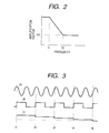
- Kh stands for an amplification factor at frequency f2 or higher of the filter circuit 7 having such a lag-lead characteristic as shown in Fig. 2, and Ko stands for a modulation frequency of VCO 12.
- Kh x Ko is measured and then the amplification factor of the variable gain portion 6 in the phase detector 4 is adjusted by trimming the resistance value so as to give a desired jitter transfer bandwidth.
- Kh x Ko is measured in the following manner.
- the test pad 22 is set so as to give a high impedance output from the variable gain portion 6 in the phase detector 4, the switch 51 is set for connection with the variable voltage source 52, and the switch 53 is set for connection with the resistor 55.
- the variable voltage source is set at voltages V1 and V2 near a voltage V0 at which the frequency of a signal outputted from a clock output pad 26 becomes equal to a lock frequency f0 of the CDR IC 27, and the frequency of a signal outputted from the clock output pad 26 is measured.
- Kh x Ko can be represented by the following Expression (2): Kh x Ko ⁇ (f2 - f1)/(V2 - V1)
- the test pad 21 is set so that the selector 3 is set to have a 45°-leading signal from the output of VCO 12 and a 45°-lagging signal from the VCO output applied to the phase detector 4 and so that the amplifier portion in the filter circuit 7 provides a high impedance output.
- the test pad 22 is set so that the variable gain portion 6 in the phase detector 4 operates as an amplifier circuit, the switch 51 is set for connection with the voltmeter 50, the switch 53 is set for connection with the voltage source 54, and the voltage source 54 is set so that the frequency of a signal outputted from the clock output pad 26 becomes f0.
- the value of the voltmeter 50 is equal to Kd x Ad, so for adjustment into a desired jitter transfer bandwidth ⁇ jt, the amplification factor of the variable gain portion 6 in the phase detector 4 is adjusted so as to be ⁇ jt/(Kh x Ko), for example, by trimming the resistance value.
- the signal 4a resulting from leading the output of VCO 12 by 45° and a signal resulting from lagging the output of VCO 12 by 45° are inputted to the phase detector 4.
- the phase detecting portion 5 in the phase detector 4 there is used a sample & hold type.
- the output signal from VCO 12 is sinusoidal, the 45°-leading signal 4a from the output of the VCO 12 and the 45°-lagging signal 4b from the VCO 12 are 90° out of phase with each other, so the output of the phase detecting portion 5 exhibits the same value of amplitude as the amplitude Vp of the output signal from VCO 12.
- the detection sensitivity of the phase detecting portion 5 in the phase detector 4 in phase-locked condition of CDR IC 27 corresponds to a gradient at t5 of the output signal from VCO 12 as in Fig. 3, so the value thereof becomes equal to the amplitude Vp of the output signal from VCO 12.
- the reading on the voltmeter 50 becomes equal to Kd x Ad, and by adjusting the value of Ad by trimming it becomes possible to adjust the jitter transfer bandwidth of CDR IC 27 to a desired value.
- the filter circuit 7 is composed of the amplifier circuit portion 8, resistor 9 in the IC and external capacitor 10 and resistor 11, it is not always necessary to adopt such a configuration insofar as there is obtained such a lag-lead characteristic as shown in Fig. 2.
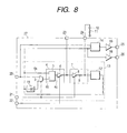
- a +90° phase shifter 17 may be connected between VCO 12 and the phase detector 4, as shown in Fig. 7. Further, as shown in Fig. 8, a -90° phase shifter 18 may be connected between the VCO 12 and the selector 3.
- the gain of the variable gain portion 6 in the phase detector 4 is changed by resistance trimming and it is thereby possible to adjust the jitter transfer bandwidth, it is not required to make adjustment at the time of assembling the module. Consequently, it becomes possible to reduce the cost of the optical receiver.
- the adjustment of the jitter transfer bandwidth can be made using the voltage sources 52, 54, the voltmeter 50 and the frequency meter 90 without using the expensive pulse pattern generator 76 and jitter analyzer 77, thus making it possible to reduce the cost of the optical receiver.
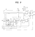
- Fig. 9 is a circuit diagram illustrating a CDR IC in an optical module according to a further embodiment of the present invention.
- the CDR IC of this embodiment comprises a PLL (phase locked loop) 13, a decision circuit 14, a data buffer 15, and a clock buffer 16, the PLL 13 comprising a +45° phase shifter 1, a -45° phase shifter 2, a frequency divider 19 connected to an output of the -45° phase shifter 2, a selector 3 for selecting either an output from a data input pad 20 or an output from the frequency divider 19, a phase detector 4, a filter circuit 7, and a VCO (voltage-controlled oscillator) 12, the phase detector 4 comprising a sample & hold type phase detecting portion 5 for comparing the phase of an output from the selector 3 with that of an output from the +45° phase shifter 1 and a variable gain portion 6 capable of changing the amplification factor by trimming the resistance value in the circuit and capable of providing a high impedance output in accordance with a signal from a test pad 21, the filter circuit comprising an amplifier circuit portion 8 capable of providing a high impedance output in accordance
- the test pad 21 is set so that the selector 3 is set to have a 45°-leading signal from the output of VCO 12 and a 45°-lagging signal from the VCO output applied to the phase detector 4 and so that the amplifier portion 8 in the filter circuit 7 provides a high impedance output.
- the test pad 22 is set so that the variable gain portion 6 in the phase detector 4 operates as an amplifier circuit, a switch 51 is set for connection with a voltmeter 50, a switch 53 is set for connection with a voltage source 54, and the voltage source 54 is set so that the frequency of a signal outputted from a clock output pad 26 becomes f0.
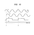
- the resulting waveform is as shown in Fig. 10.
- indicated at 4a is the waveform of an input 4a of the phase detector 4 obtained by causing the output of VCO 12 to lead 45°
- indicated at 2a is the waveform of an output 2a of the phase shifter 2 obtained by causing the output of VCO 12 to lag 45°
- indicated at 19a is the waveform of an output 19a of the frequency divider 19 obtained by dividing the waveform 2a to a half with the frequency divider 19
- indicated at 4c is the waveform of an output 4c of the phase detecting portion 5 in the phase detector 4.
- the output of the phase detecting portion 5 takes the same value as the amplitude Vp of an output signal from VCO 12 and thus it is possible to obtain a detection sensitivity of the phase detecting portion 5.
- the frequency thereof is a half or less of the signal 4b in jitter transfer bandwidth adjustment which signal is a clock signal. That is, the circuit in which the signal 4b is inputted in the phase detecting portion 5 of the phase detector 4 requires an operating frequency twice as high as that in normal operation, so that there occurs a wasteful portion in the circuit due to the resulting necessity of allowing a large amount of current to flow to permit a high-speed operation.
- Fig. 9 there are used both +45° and -45° phase shifters, there may be used a +90° or -90° phase shifter as in Figs. 7 and 8.
- Fig. 15 is a configuration diagram using a CDR IC according to a further embodiment of the present invention.
- a server or router 88 is composed of a substrate with plural multiplexers 80 and transmission line drivers 81 mounted thereon, a substrate 87 with plural receiving amplifiers 82, CDR ICs 83 and demultiplexers 84 mounted thereon, and plural transmission lines 85 for connection between both substrates.
- the transmission lines 85 are, for example, coaxial or twisted pair cables or lines formed on a substrate.
- a signal exceeding 1GHz is allowed to flow in the transmission lines 85 for increasing the amount of data transmitted between the substrates and for decreasing the number of cables and of signal lines on the substrates to reduce the manufacturing cost. With such a signal exceeding 1GHz, it is difficult to phase data and clock with each other and therefore only the data signal is transmitted, while clock is reproduced in the CDR IC 83.
- a jitter standard is established as is the case with the optical receiver and for observing the standard it is necessary to adjust the jitter transfer bandwidth. Since plural CDR ICs are mounted on a substrate, several ten minutes to several hours are needed for the adjustment, but according to the present invention all that is required is a mere mounting of IC, thus making it possible to reduce the cost of the server or router.
- the cost for adjustment at the time of assembling the optical module is reduced, thereby permitting the provision of a less expensive optical module.
Landscapes
- Engineering & Computer Science (AREA)
- Computer Networks & Wireless Communication (AREA)
- Signal Processing (AREA)
- Stabilization Of Oscillater, Synchronisation, Frequency Synthesizers (AREA)
- Optical Communication System (AREA)
- Light Receiving Elements (AREA)
- Dc Digital Transmission (AREA)
Applications Claiming Priority (2)
| Application Number | Priority Date | Filing Date | Title |
|---|---|---|---|
| JP2001192704 | 2001-06-26 | ||
| JP2001192704A JP4426739B2 (ja) | 2001-06-26 | 2001-06-26 | 光モジュールおよびその製造方法 |
Publications (3)
| Publication Number | Publication Date |
|---|---|
| EP1271838A2 true EP1271838A2 (fr) | 2003-01-02 |
| EP1271838A3 EP1271838A3 (fr) | 2005-03-16 |
| EP1271838B1 EP1271838B1 (fr) | 2007-10-10 |
Family
ID=19031119
Family Applications (1)
| Application Number | Title | Priority Date | Filing Date |
|---|---|---|---|
| EP01306830A Expired - Lifetime EP1271838B1 (fr) | 2001-06-26 | 2001-08-10 | Procédés et dispositives d'amélioration de transfer de gigue dans de modules optiques |
Country Status (4)
| Country | Link |
|---|---|
| US (1) | US6979810B2 (fr) |
| EP (1) | EP1271838B1 (fr) |
| JP (1) | JP4426739B2 (fr) |
| DE (1) | DE60130875T2 (fr) |
Families Citing this family (5)
| Publication number | Priority date | Publication date | Assignee | Title |
|---|---|---|---|---|
| US7343535B2 (en) | 2002-02-06 | 2008-03-11 | Avago Technologies General Ip Dte Ltd | Embedded testing capability for integrated serializer/deserializers |
| US20050063431A1 (en) * | 2003-09-19 | 2005-03-24 | Gallup Kendra J. | Integrated optics and electronics |
| US7520679B2 (en) | 2003-09-19 | 2009-04-21 | Avago Technologies Fiber Ip (Singapore) Pte. Ltd. | Optical device package with turning mirror and alignment post |
| US6953990B2 (en) | 2003-09-19 | 2005-10-11 | Agilent Technologies, Inc. | Wafer-level packaging of optoelectronic devices |
| US6982437B2 (en) | 2003-09-19 | 2006-01-03 | Agilent Technologies, Inc. | Surface emitting laser package having integrated optical element and alignment post |
Family Cites Families (8)
| Publication number | Priority date | Publication date | Assignee | Title |
|---|---|---|---|---|
| DE19740957C2 (de) * | 1997-09-17 | 1999-08-19 | Fraunhofer Ges Forschung | Vorrichtung und Verfahren zur Takt- und Trägerrückgewinnung |
| CA2220622C (fr) * | 1997-11-03 | 2004-03-30 | Aubin P. J. Roy | Methode et circuit d'autocontrole integre de boucles de verrouillage de phase |
| US6298103B1 (en) * | 1998-06-16 | 2001-10-02 | Sorrento Networks Corporation | Flexible clock and data recovery module for a DWDM optical communication system with multiple clock rates |
| JP3573975B2 (ja) * | 1998-10-23 | 2004-10-06 | 日本オプネクスト株式会社 | 光受信器、位相同期ループ回路、電圧制御発振器および周波数応答可変増幅器 |
| CA2361002C (fr) * | 1999-01-28 | 2005-07-26 | California Institute Of Technology | Techniques optoelectroniques de reduction de bruit de phase par suppression de porteuse dans un signal de porteuse |
| US6631144B1 (en) * | 1999-12-21 | 2003-10-07 | Intel Corporation | Multi-rate transponder system and chip set |
| JP2002016493A (ja) * | 2000-06-30 | 2002-01-18 | Hitachi Ltd | 半導体集積回路および光伝送用送信回路 |
| DE60231266D1 (de) * | 2001-03-07 | 2009-04-09 | Nippon Telegraph & Telephone | Schaltung zur Daten-und Taktrückgewinnung |
-
2001
- 2001-06-26 JP JP2001192704A patent/JP4426739B2/ja not_active Expired - Lifetime
- 2001-08-10 EP EP01306830A patent/EP1271838B1/fr not_active Expired - Lifetime
- 2001-08-10 DE DE60130875T patent/DE60130875T2/de not_active Expired - Lifetime
- 2001-08-15 US US09/930,806 patent/US6979810B2/en not_active Expired - Fee Related
Also Published As
| Publication number | Publication date |
|---|---|
| US6979810B2 (en) | 2005-12-27 |
| US20040067068A1 (en) | 2004-04-08 |
| EP1271838A3 (fr) | 2005-03-16 |
| JP2003008049A (ja) | 2003-01-10 |
| EP1271838B1 (fr) | 2007-10-10 |
| JP4426739B2 (ja) | 2010-03-03 |
| DE60130875D1 (de) | 2007-11-22 |
| DE60130875T2 (de) | 2008-07-17 |
Similar Documents
| Publication | Publication Date | Title |
|---|---|---|
| US7224911B2 (en) | Adaptive distortion compensation in optical fiber communication networks | |
| US6463109B1 (en) | Multiple channel adaptive data recovery system | |
| US8040940B2 (en) | Transmitter/receiver device that converts serial and parallel signals and method of testing thereof | |
| US7853836B2 (en) | Semiconductor integrated circuit | |
| US20050108600A1 (en) | Process and device for testing a serializer circuit arrangement and process and device for testing a deserializer circuit arrangement | |
| US7860472B2 (en) | Receiver circuit and receiver circuit testing method | |
| US8861979B2 (en) | Coherent receiver apparatus and chromatic dispersion compensation method | |
| US7743288B1 (en) | Built-in at-speed bit error ratio tester | |
| US6950972B2 (en) | Multi-purpose BER tester (MPBERT) for very high RZ and NRZ signals | |
| US20040125902A1 (en) | Phase shifter, phase shifting method and skew compensation system for high-speed parallel signaling | |
| US5870211A (en) | Error rate measurement system for high speed optical pulse signals | |
| EP1271838A2 (fr) | Procédés et dispositives d'amélioration de transfer de gigue dans de modules optiques | |
| US7783206B2 (en) | System and method for multi-rate, high-sensitivity clock and data recovery with adjustable decision threshold, RF input, and optical-to-electrical conversion | |
| JP4690854B2 (ja) | ソース同期サンプリング方法 | |
| US20030180051A1 (en) | Wavelength division multiplex transmission system or a polarisation division multiplex system with means for measuring dispersion characteristics, an optical transmitter, an optical receiver and a method therefore | |
| EP1445880B1 (fr) | Régénérateur pour signaux électriques | |
| US6901225B1 (en) | Device for detecting polarization mode dispersions | |
| JP2003008431A (ja) | クロック・データリカバリicおよびそのジッタ伝達帯域調整方法 | |
| CN110958057B (zh) | 用于待测装置dut的时间信号测量的系统和方法以及形成系统的方法 | |
| US20100128804A1 (en) | Automatic Phase Shifter and Aligner for High-Speed Serial Data | |
| JP3543757B2 (ja) | 識別位相自動調整方法及び方式並びにこれを備えた光受信器 | |
| Nishitani et al. | Optical serial highway for CAMAC system using high-performance optical bus adapters | |
| CN120185993A (zh) | 时间频率信号调制传输方法及系统 | |
| CARD | Optical and High Speed Networking | |
| Davidson et al. | High speed QPPM direct detection optical communication receivers for FSDD intersatellite links |
Legal Events
| Date | Code | Title | Description |
|---|---|---|---|
| PUAI | Public reference made under article 153(3) epc to a published international application that has entered the european phase |
Free format text: ORIGINAL CODE: 0009012 |
|
| 17P | Request for examination filed |
Effective date: 20010830 |
|
| AK | Designated contracting states |
Kind code of ref document: A2 Designated state(s): AT BE CH CY DE DK ES FI FR GB GR IE IT LI LU MC NL PT SE TR |
|
| AX | Request for extension of the european patent |
Free format text: AL;LT;LV;MK;RO;SI |
|
| PUAL | Search report despatched |
Free format text: ORIGINAL CODE: 0009013 |
|
| AK | Designated contracting states |
Kind code of ref document: A3 Designated state(s): AT BE CH CY DE DK ES FI FR GB GR IE IT LI LU MC NL PT SE TR |
|
| AX | Request for extension of the european patent |
Extension state: AL LT LV MK RO SI |
|
| AKX | Designation fees paid |
Designated state(s): DE FR GB |
|
| GRAP | Despatch of communication of intention to grant a patent |
Free format text: ORIGINAL CODE: EPIDOSNIGR1 |
|
| GRAS | Grant fee paid |
Free format text: ORIGINAL CODE: EPIDOSNIGR3 |
|
| GRAA | (expected) grant |
Free format text: ORIGINAL CODE: 0009210 |
|
| AK | Designated contracting states |
Kind code of ref document: B1 Designated state(s): DE FR GB |
|
| REG | Reference to a national code |
Ref country code: GB Ref legal event code: FG4D |
|
| REF | Corresponds to: |
Ref document number: 60130875 Country of ref document: DE Date of ref document: 20071122 Kind code of ref document: P |
|
| ET | Fr: translation filed | ||
| PLBE | No opposition filed within time limit |
Free format text: ORIGINAL CODE: 0009261 |
|
| STAA | Information on the status of an ep patent application or granted ep patent |
Free format text: STATUS: NO OPPOSITION FILED WITHIN TIME LIMIT |
|
| 26N | No opposition filed |
Effective date: 20080711 |
|
| GBPC | Gb: european patent ceased through non-payment of renewal fee |
Effective date: 20080810 |
|
| PG25 | Lapsed in a contracting state [announced via postgrant information from national office to epo] |
Ref country code: GB Free format text: LAPSE BECAUSE OF NON-PAYMENT OF DUE FEES Effective date: 20080810 |
|
| PGFP | Annual fee paid to national office [announced via postgrant information from national office to epo] |
Ref country code: DE Payment date: 20140806 Year of fee payment: 14 |
|
| PGFP | Annual fee paid to national office [announced via postgrant information from national office to epo] |
Ref country code: FR Payment date: 20140808 Year of fee payment: 14 |
|
| REG | Reference to a national code |
Ref country code: DE Ref legal event code: R119 Ref document number: 60130875 Country of ref document: DE |
|
| REG | Reference to a national code |
Ref country code: FR Ref legal event code: ST Effective date: 20160429 |
|
| PG25 | Lapsed in a contracting state [announced via postgrant information from national office to epo] |
Ref country code: DE Free format text: LAPSE BECAUSE OF NON-PAYMENT OF DUE FEES Effective date: 20160301 |
|
| PG25 | Lapsed in a contracting state [announced via postgrant information from national office to epo] |
Ref country code: FR Free format text: LAPSE BECAUSE OF NON-PAYMENT OF DUE FEES Effective date: 20150831 |