EP1273015B1 - PROCEDE POUR ISOLER UN SUPRACONDUCTEUR A HAUTE Tc, ET APPLICATION DE CE PROCEDE - Google Patents
PROCEDE POUR ISOLER UN SUPRACONDUCTEUR A HAUTE Tc, ET APPLICATION DE CE PROCEDE Download PDFInfo
- Publication number
- EP1273015B1 EP1273015B1 EP01909542A EP01909542A EP1273015B1 EP 1273015 B1 EP1273015 B1 EP 1273015B1 EP 01909542 A EP01909542 A EP 01909542A EP 01909542 A EP01909542 A EP 01909542A EP 1273015 B1 EP1273015 B1 EP 1273015B1
- Authority
- EP
- European Patent Office
- Prior art keywords
- conductor
- superconductor
- strip form
- sheathed
- sheathing
- Prior art date
- Legal status (The legal status is an assumption and is not a legal conclusion. Google has not performed a legal analysis and makes no representation as to the accuracy of the status listed.)
- Expired - Lifetime
Links
Images

Classifications
-
- H—ELECTRICITY
- H01—ELECTRIC ELEMENTS
- H01B—CABLES; CONDUCTORS; INSULATORS; SELECTION OF MATERIALS FOR THEIR CONDUCTIVE, INSULATING OR DIELECTRIC PROPERTIES
- H01B13/00—Apparatus or processes specially adapted for manufacturing conductors or cables
- H01B13/06—Insulating conductors or cables
- H01B13/14—Insulating conductors or cables by extrusion
Definitions
- the invention relates to a corresponding method and to the process enveloped high-T c superconductor.
- HTS conductors with oxide high-T c superconducting material (HTS material).
- HTS conductors which have a wire form (with a circular cross-section) and in particular a band shape (with rectangular cross-section) can be provided in an easy to be carried out process continuously with an insulating sheath.
- the method should be suitable both for a single-conductor insulation as well as for the isolation of a HTS conductor structure in the form of a multi-conductor, which is composed of superconducting individual conductors, or a composite conductor with superconducting and normal conducting parts.
- the so-called degree of stretching ie the stretching of the material
- the stretching can advantageously take place under the simultaneous action of vacuum inside the tube. Together with an advantageous preheating of the conductor before the inlet into the guide channel and / or during the pulling of the conductor through this can thus produce a particularly good and bubble-free adhesive fit of the envelope on the superconductor.
- the then taking place slow Ablung z. B. in air causes freezing and stress-free solidification of the melt from the insulating material on the conductor.
- coating installations are known, by means of which insulating sheathings made of a thermoplastic material (see DE 26 38 763 A) by stripping nozzles, in pressure jacket or in the hose-stretching method (DE 24 09 655 A, 20 22 802 A, DE 21 10 934 A ) are to be applied to wires.
- the wires can in this case consist in particular of steel (compare US Pat. No. 3,893,642), A1 (cf DE 24 09 655 A) or Cu (cf US Pat. No. 4,489,130 or the cited DE 21 10 934 A) and are generally circular cross-sectional areas.
- the coating process to be carried out with such equipment is also referred to as extrusion coating.
- a band shape of the superconductor of importance should be understood to mean any rectangular shape with angular or rounded edges.
- the rectangular shape can have a relatively high aspect ratio, generally greater than 10, as is the case in particular with known thin HTS ribbon conductors.
- the proposed method a continuous coating of a HTS conductor is possible, since the insulation material can be conveyed from a reservoir, which can be refilled at any time.
- the thickness of the insulating sheath in a wide range is variable and adjust with sufficient accuracy. Since, for example, each individual conductor can be completely insulated, a double insulation security is given for strip conductor windings because the conductors are separated by a double insulation layer.
- the mechanical and thermal property profile of the envelope can be adapted to the particular application by the use of different thermoplastic materials.
- the proposed method is significantly faster than a conventional metallic Umspinnungs- or Lackiermaschine in metallic superconductors.
- the lateral conductor edges are isolated, so that the risk of short circuits in this area is reduced.
- the insulation is particularly suitable for thin band conductors with unfavorable aspect ratio. This eliminates the dreaded during painting process danger of a so-called "edge escape", i. an unwanted thick layer dilution in the range of edges with small edge radii, as they are given just with thin conductor strips.
- the HTS conductor does not need to be mechanically stressed too much.
- the mechanical load is limited to the low tensile forces generated by Leiterabwickler or -aufwickler. A conductor deflection during the coating process can thus be advantageously avoided.
- thermoplastic materials are to be used with relatively low processing or melting temperature of less than 200 ° C and only a relatively short-term heating of the conductors are provided so as to a degradation of the superconducting properties (with respect to the critical temperature T c and in particular with regard to the critical current density J c to be measured in A / m 2, at least largely avoided.
- Suitable thermoplastic materials for this purpose are polyethylenes, Polystyrene-ethylene-butylene elastomers, polyurethane elastomers, ethylene / vinyl acetate copolymers or acrylic acid / acrylate copolymers have been proposed.
- insulating layer thicknesses of at least about 40 to 50 ⁇ m can be realized.
- the insulating layer should be lower contrast.
- a good adhesion of the insulating material on the conductor and a good connection of the corresponding insulating layer of impregnating and casting resins should be ensured.
- Object of the present invention is therefore to propose a method which reduces the aforementioned difficulties.
- special, enveloped by the process high-T c superconductors are given.
- thermoplastics are in particular special engineering thermoplastics such as polyamides and polyesters and in particular high-temperature thermoplastics (HT thermoplastics) such as polyetherimide (PEI), polyethersulfone (PES), polysulfone (PSU), polyphenylene sulfone (PPSU) and polyetheretherketone (PEEK) suitable.
- HT thermoplastics high-temperature thermoplastics
- PEI polyetherimide
- PES polyethersulfone
- PSU polysulfone
- PPSU polyphenylene sulfone
- PEEK polyetheretherketone
- HTS strip conductors in particular with filaments of Bi cuprate material and an embedding of the filaments in an Ag matrix, can withstand temperatures of at least 500 ° C. for several minutes without impairing their superconducting properties, in particular their current carrying capacity.
- thermoplastics can be selected according to the invention.
- inventively selected thermoplastics especially the HT thermoplastics PEI, PPSU and PEEK, have very good electrical and exceptionally good low temperature properties, ie, by good flexibility and toughness at low Distinguish temperatures.
- other thermoplastics often show a strong tendency to embrittle at low temperatures.
- thermoplastics proposed by the earlier application WO 00/11684 are improved adhesion adhesion to ceramic and metallic substrates to be achieved in the claimed temperature range due to the pronounced polar character of these materials and the significantly better compatibility and bonding to epoxide (EP) ) and unsaturated polyester resins (UP resins) used as potting and impregnating compositions for use of such superconductors.
- EP epoxide
- UP resins unsaturated polyester resins
- thermoplastics to be selected according to the invention advantageously have a high modulus of elasticity (> 3000 MPa) at room temperature, a high surface hardness (Rockwell hardness ⁇ 120, R scale) and a low coefficient of friction ( ⁇ 0.6).
- EVA ethylene vinyl acetate
- modulus ⁇ 400 Mpa modulus ⁇ 400 Mpa
- surface hardness Shore D ⁇ 40 surface hardness Shore D ⁇ 40
- friction coefficient> 1 This mechanical and tribological property profile of the selected Thermoplastics also enable problem-free production of Roebelleitern.
- a significant advantage of using the new insulating materials lies in the significant reduction of the insulating layer thickness. Due to the good processing properties of these plastics in the tube stretching process can allow insulating layer of the cladding of less than 100 ⁇ m, preferably in the range 15 to 30 ⁇ m and realize including, for example microns average thickness of not more than 30th This is essential to achieve a high effective current density in the conductor. Compared with the materials according to the previous application WO 00/11684, where preferably with a layer thickness of about 50 ⁇ is worked m, this is a reduction of the layer thickness of over 50%.
- the combination of good processing behavior and the above-mentioned mechanical and tribological property profile enables the safe and problem-free production preferably of Roebelleitern with insulating layer thicknesses of 15 to 30 ⁇ m with high effective current density.
- HTS conductor to which the method according to the invention is to be applied is here understood to mean not only a single conductor, but also a composition of several such conductors or parts of them.
- the conductor can contain at least one conductor core made of the superconducting material.
- An inventive coated with an insulating sheath superconductor can be used without additional insulation film. Thus eliminates caused by the co-winding insulation isolation effort.
- casings with an approximately uniform thickness on all sides can advantageously be formed with the method according to the invention.
- a designed outlet opening of the nozzle can provide that their spacing is uneven with respect to the conductor in its circumferential direction. In this way, in particular certain distances between adjacent conductors, for example within a conductor network or a winding can be determined.
- the method according to the invention can just as well be used for wrapping band-shaped superconducting multiple or composite conductors.
- Such conductors have a structure of a plurality of superconducting conductor parts or conductor regions, wherein at least one superconducting single conductor or such a conductor core are provided.
- a corresponding structure can be particularly simply and evenly provided with an insulating sheath with the inventive method without the risk of affecting the conductor properties of the superconductor material.
- the heating temperature should preferably be at least approximately the process temperature (permissible deviation: +/- 50 ° C).
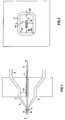
- Figures 1 and 2 show a nozzle of a system for carrying out the method according to the invention as a longitudinal section or in front view such as FIG. 3 shows a plant for the extrusion coating of a HTS conductor with a nozzle according to FIGS. 1 and 2.
- a system to be provided for carrying out the method according to the invention is based on devices known per se, such as those used for coating non-superconducting wires with plastic materials by means of extrusion coating according to the so-called tube stretching method (see the aforementioned US 3,893,642 or the cited US Pat DE-A-2 022 802 and 21 10 934).
- a corresponding system (see Figure 3) comprises a so-called extruder with extrusion head, which has an extrusion die, which is illustrated in Figures 1 and 2 in longitudinal section and in front view.
- This nozzle generally designated 2 contains a guide channel 3 centrally through this channel, a superconductor 5 to be provided with an electrically insulating sheath 4 is to be guided in a direction of advance indicated by an arrow v by means of propulsion means (see FIG.
- the superconductor 5 is a band-shaped HTS conductor. This conductor can advantageously be preheated prior to insertion into the guide channel 3.
- the guide channel itself can be heated.
- the insulating material of the envelope 4 is melted in the extruder (see FIG. 3), not shown, conveyed into the extrusion head with distribution system and pressed as a melt 6 into a die gap 7 of the extrusion die 2.
- the gap width is significantly greater than the final thickness d of the sheath 4 to the strip conductor 5, occurs in the advancing v seen a melt tube 9, in the form of a stretch cone due to a fixation of its apex on the strip conductor stretched and applied with the required on the stripline layer thickness d on the conductor.
- the nozzle gap opening 8 advantageously has a shape adapted to the contour of the strip conductor 5 form.
- the thus largely rectangular opening with rounding at the corners is spaced with respect to the surfaces of the strip conductor by distances a1 and a2 and is defined by gap widths w1 and w2 and by radii of curvature R1 and R2 in their corner regions.
- the distances (a1, a2) of the nozzle gap opening 8 from the strip conductor 5, their geometric configuration (w1, w2, R1, R2) and the advancing speed v of the conductor determine the contour of the envelope 4 and its thickness d.
- the geometric design of the extrusion die can, as was assumed for the embodiment of Figure 2, are chosen so that the thickness d of the envelope 4 is about the same size on all sides.
- a thickness d of less than 0.5 mm is planned, for example between 30 and 300 ⁇ m.
- Deviating from it can by a Another design of the extrusion nozzle opening, for example a2 ⁇ a1 and w1 ⁇ w2, causes side lips to form on the narrow sides of the conductor. Such side lips can then be used as spacers in the manufacture of layer windings and thus make an additional co-winding of special spacers such as glass twine superfluous.
- the contour of the outlet opening 8 of the nozzle gap may be structured such that a non-uniform thickness of the envelope results on at least one side of the conductor. In this way, for example, by means of a groove-like depression in the contour of the opening 8 to obtain a web-like bead of the envelope, which can then serve as a spacer. Furthermore, it is also possible, if appropriate, to disregard an exactly centric guidance of the superconductor through the guide channel 3 in order to produce a one-sided or two-sided stronger covering.
- Suitable insulating plastic materials for the sheath 4 are all thermoplastic materials which, on the one hand, have a processing or melting temperature which precludes impairment of the superconducting properties of the HTS conductor 5 to be enveloped and nevertheless ensures adequate plasticity for the extrusion coating process. It has surprisingly been found that known HTS ribbon conductors with filaments of Bi cuprate material embedded in an Ag matrix can withstand temperature stresses of over 500 ° C. for several minutes without impairing their superconducting properties. A corresponding concrete HTS standard strip conductor on which the following considerations are based is known from "IEEE Transactions on Applied Superconductivity", Vol. 2, June 1999, pages 2480 to 2485.
- thermoplastic materials whose processing temperature is above 200 ° C. and can amount to a maximum of 500 ° C. are preferably selected for such a HTS ribbon conductor.
- those materials are selected which allow processing in a temperature range between 220 ° C and 450 ° C, in particular between 240 ° C and 420 ° C, preferably between 250 ° C and 380 ° C.
- the choice of thermoplastics for this temperature range is particularly large.
- suitable materials are, in particular, known technical thermoplastics from the family of polyamides or polyesters, which are preferably to be provided for the lower part (approximately between 200 ° C. and 290 ° C.) of the temperature range mentioned.
- thermoplastics such as a polyetherimide (PEI) or a polyethersulfone (PES) or a polysulfone (PSU) or a polyphenylene sulfone (PPSU) or a polyetheretherketone (PEEK) ,
- PEI polyetherimide
- PES polyethersulfone
- PSU polysulfone
- PPSU polyphenylene sulfone
- PEEK polyetheretherketone
- thermoplastic insulation materials are additionally made from the viewpoint that the thermoplastics used have sufficiently good low-temperature properties so as to exclude failures under operating conditions and / or during cooling and warm-up operations.
- the insulating sleeve can additionally be dyed with dyes. As a result, a slight optical control of the envelope is possible.
- the thin-film extrusion coating process according to the invention is particularly suitable for wrapping band-shaped HTS conductors whose conductor strip thickness is less than 1.5 mm, preferably less than 0.5 mm, and which have a high aspect ratio of at least 3, preferably at least 10.
- a corresponding HTS ribbon conductor may, for example, have a width of 3.6 mm and a thickness of 0.25 mm, and in particular be the aforementioned HTS standard ribbon conductor.
- bi-cuprate materials which contain mainly the so-called 2212 phase (80 K phase) or preferably the so-called 2223 phase (110 K phase) at least predominantly (cf. eg "IEEE Transactions on Applied Superconductivity ", Vol. 7, No. 2, June 1997, pages 355 to 358).
- the bi-cuprate material may additionally contain Pb (so-called "BPSCCO").
- Band-shaped HTS conductors with sheaths produced according to the invention are also usually provided with an additional ceramic surface coating which is intended to prevent sintering of the actual, metallic outer sides or surfaces of the conductor, which preferably consist of Ag or an Ag alloy such as AgMg, during required reaction anneals ,
- a corresponding 2223 BPSCCO / Ag standard tape conductor was wrapped with a thermoplastic material according to the invention.
- a corresponding coating system is indicated in FIG.
- This system has the following parts in succession in the direction of tape guide v, namely an unwinding device (so-called “unwinder") 14, from which the HTS strip conductor 5 to be coated is unwound, a felt brake 15, an N 2 protective gas purge 16 to prevent oxidation, a non-contact inductive heating conductor 17 to the conductor at least approximately to the processing temperature of the used thermoplastic insulation material such as from a thermoplastic polyurethane elastomer, an extrusion coater (so-called “extruder”) 18 with a refilling funnel 19 for the thermoplastic insulating material, an extrusion head with a built-in extrusion die 2, an air shower 20, a plurality of guide rollers 21i, a pore detector 22 for monitoring the applied envelope, at least one cold air blower 23j,
- the thickness d of the enclosure can also be influenced by the choice of a suitable tape withdrawal speed, the thickness d of the enclosure.
- a suitable tape withdrawal speed for example, at a conductor throughput speed of about 5 m / min, an envelope of about 30 microns thickness can be generated.
- To improve adhesion of the envelope on the conductor surface of the conductor by means of the conductor heating 17 is inductively preheated, in particular at least approximately to a temperature level near the processing temperature (ie, possibly slightly above or below, eg +/- 50 ° C).
- This preheating of the conductor which is only required for a short time and therefore does not damage the superconductor material, is advantageously carried out under a protective gas atmosphere in order to avoid oxide formations on the conductor surface, which can have a negative effect on the adhesion of the insulating coating layer on the conductor.
- a possible preheating of a conductor is indeed known prizipiell; however, the previously used preheating temperatures are significantly lower than the processing temperatures of the selected thermoplastics to be provided for HTS conductors. To have a really good adhesive bond To ensure the insulating material on the conductor, a conductor preheating to the highest possible temperature is appropriate in which a HTS conductor damage respect. Its superconducting properties does not occur.
- thermoplastic insulating material During the subsequent coating process, the air nozzles of the air shower 20 mounted behind the extruder 18, any countercurrent cooler still present and the fan 23j serve for faster cooling and solidification of the applied coating layer of the thermoplastic insulating material.
- an on-line test for insulation failure by a non-destructive working pore detector 22 and a monitoring of the applied insulating layer thickness for example by means of laser assembly 24. Due to the rapid cooling and solidification of the envelope can gluing the shells during subsequent winding of the conductor 5 'on the winder 26th be prevented.
- a release layer for example made of paper with the conductor on the reel serving as a supply reel 26 to exclude there gluing of the conductor during storage.
- the sheath of the conductor can be provided with a suitable powder, for example talc.
- Example 1 Application of the insulating layer according to the method described above with PEEK insulation
- Processing temperature melt 380 ° C conductor preheating: 375 ° C Isolation from PEI processing temperature Melt: 370 ° C conductor preheating: 370 ° C Isolation from PPSU processing temperature Melt: 375 ° C conductor preheating: 370 ° C
- Example 4 electrical properties at 77 K in liquid nitrogen
- Partial discharge conductor / conductor Breakdown of conductor / conductor Partial discharge conductor / edge Punch conductor / edge PEEK (25 ⁇ m) 5500 V 15000 V 3000 V 4000 V PPSU (25 ⁇ m) 3200 V 12000 V 2500V 6300V EVA (50 ⁇ m) 3000 V 8000 V 2700 V 3500 V
- EVA values represent comparative values obtained in the process proposed by the aforementioned WO document.
Landscapes
- Engineering & Computer Science (AREA)
- Manufacturing & Machinery (AREA)
- Superconductors And Manufacturing Methods Therefor (AREA)
- Manufacture Of Macromolecular Shaped Articles (AREA)
- Extrusion Moulding Of Plastics Or The Like (AREA)
- Superconductor Devices And Manufacturing Methods Thereof (AREA)
Claims (21)
- Procédé d'obtention d'un enrobage de tous côtés en une matière plastique isolante du point de vue électrique d'au moins un supraconducteur en forme de bande ayant une matière supraconductrice oxydée à Tc haute, dans lequel dans une opération d'enrobage continu à une température du procédé n'influant pratiquement pas sur les propriétés de supraconduction du conducteur,- on fait sortir le conducteur d'un canal de guidage s'étendant dans une direction d'avance,- on extrude un tube souple fondu en une matière isolante thermoplastique fondue dans la direction d'avance d'une buse dont l'orifice de sortie entoure le conducteur en étant à distance de tous côtés,- par l'avance du conducteur, le tube souple fondu est allongé et est tiré sur la surface du conducteur,
ainsi que- on solidifie par refroidissement le tube souple fondu déposé à la surface du conducteur,procédé dans lequel on utilise, à une température du procédé comprise entre 200°C et 500°C, de préférence entre 220°C et 450°C, comme matière isolante une matière thermoplastique dont le point de fusion est dans cette plage de températures. - Procédé suivant la revendication 1, caractérisé en ce que l'on prévoit une température du procédé comprise entre 240°C et 420°C, de préférence entre 250°C et 380°C.
- Procédé suivant la revendication 1 ou 2, caractérisé en ce que l'on prévoit comme matière isolante un polyamide ou un polyester.
- Procédé suivant la revendication 1 ou 2, caractérisé en ce que l'on prévoit comme matière isolante un polyétherimide (PEI) ou une polyéthersulfone (PES) ou une polysulfone (PSU) ou une polyphénylènesulfone (PPSU) ou une polyétheréthercétone (PEEK).
- Procédé suivant l'une des revendications précédentes, caractérisé en ce que l'on porte le conducteur (5) avant ou lors de l'entrée dans le canal (3) de guidage au moins à peu près à la température du procédé.
- Procédé suivant la revendication 5, caractérisé en ce que l'on chauffe le canal (3) de guidage.
- Procédé suivant la revendication 5 ou 6, caractérisé en ce que l'on chauffe le conducteur (5) sous une atmosphère de gaz protecteur.
- Procédé suivant l'une des revendications précédentes, caractérisé en ce que, pour déposer le tube (9) souple fondu à la surface du conducteur, on fait le vide à l'intérieur du tube souple.
- Procédé suivant l'une des revendications précédentes, caractérisé en ce que l'on allonge le tube (9) souple fondu d'un degré d'étirage compris entre 5 et 15.
- Procédé suivant l'une des revendications précédentes, caractérisé en ce que l'on soumet le conducteur (5') sorti de la buse (2) et muni de l'enrobage (4) à un traitement de refroidissement.
- Procédé suivant l'une des revendications précédentes, caractérisé en ce que l'on prévoit un orifice (8) de sortie de la buse (2) tel que sa distance au conducteur (5), considéré dans sa direction de pourtour, n'est pas uniforme.
- Procédé suivant l'une des revendications précédentes, caractérisé en ce que l'on constitue un enrobage (4) d'une épaisseur (d) moyenne de 100 µm au plus, de préférence de 30 µm au plus.
- Supraconducteur à Tc haute en forme de bande enrobée suivant le procédé selon l'une des revendications précédentes, caractérisé par un rapport d'aspect d'au moins 3, de préférence d'au moins 10.
- Supraconducteur à Tc haute en forme de bande enrobée suivant la revendication 13, caractérisé par une épaisseur de bande de 1,5 mm au plus, de préférence de 0,5 mm au plus.
- Supraconducteur à Tc haute en forme de bande enrobée suivant la revendication 13 ou 14, caractérisé par plusieurs âmes de conducteur en la matière supraconductrice à Tc haute incorporée dans une matière de conduction normale.
- Supraconducteur à Tc haute en forme de bande enrobée suivant l'une des revendications 1 à 12, caractérisé par une constitution sous la forme d'un conducteur supraconducteur multifilaire ou composite qui comprend au moins un conducteur individuel supraconducteur ou une âme conductrice supraconductrice.
- Supraconducteur à Tc haute en forme de bande enrobée suivant la revendication 16, caractérisé en ce que le au moins un conducteur individuel a plusieurs âmes conductrices en la matière supraconductrice à Tc haute incorporée dans une matière de conduction normale.
- Supraconducteur à Tc haute en forme de bande enrobée suivant l'une des revendications 13 à 17, caractérisé par un enrobage (4) dont l'épaisseur (d) sur au moins deux côtés du conducteur est de 0,03 mm au plus.
- Supraconducteur à Tc haute en forme de bande enrobée suivant l'une des revendications 13 à 18, caractérisé par un enrobage (4) dont l'épaisseur (d) est plus grande sur les petits côtés du conducteur que sur les grands côtés.
- Supraconducteur à Tc haute en forme de bande enrobée suivant l'une des revendications 13 à 19, caractérisé en ce que la matière supraconductrice est en cuprate de Bi qui est incorporé dans une matière conductrice normale contenant au moins de l'Ag.
- Supraconducteur à Tc haute en forme de bande enrobée suivant l'une des revendications 13 à 20, caractérisé par une structure sous la forme d'un conducteur en barre Roebel dont les supraconducteurs (5) en forme de bandes sont enrobés respectivement individuellement.
Applications Claiming Priority (3)
| Application Number | Priority Date | Filing Date | Title |
|---|---|---|---|
| DE10006537 | 2000-02-15 | ||
| DE10006537 | 2000-02-15 | ||
| PCT/DE2001/000355 WO2001061712A1 (fr) | 2000-02-15 | 2001-01-30 | PROCEDE POUR ISOLER UN SUPRACONDUCTEUR A HAUTE Tc, ET APPLICATION DE CE PROCEDE |
Publications (2)
| Publication Number | Publication Date |
|---|---|
| EP1273015A1 EP1273015A1 (fr) | 2003-01-08 |
| EP1273015B1 true EP1273015B1 (fr) | 2006-06-28 |
Family
ID=7630878
Family Applications (1)
| Application Number | Title | Priority Date | Filing Date |
|---|---|---|---|
| EP01909542A Expired - Lifetime EP1273015B1 (fr) | 2000-02-15 | 2001-01-30 | PROCEDE POUR ISOLER UN SUPRACONDUCTEUR A HAUTE Tc, ET APPLICATION DE CE PROCEDE |
Country Status (7)
| Country | Link |
|---|---|
| US (1) | US6921445B2 (fr) |
| EP (1) | EP1273015B1 (fr) |
| JP (1) | JP4018904B2 (fr) |
| AT (1) | ATE332008T1 (fr) |
| DE (2) | DE10103324A1 (fr) |
| DK (1) | DK1273015T3 (fr) |
| WO (1) | WO2001061712A1 (fr) |
Cited By (2)
| Publication number | Priority date | Publication date | Assignee | Title |
|---|---|---|---|---|
| DE102009047865A1 (de) | 2009-09-30 | 2011-03-31 | Siemens Aktiengesellschaft | Verfahren zum Aufbringen von Kunststoff auf Einzelleiter und HTS-Verbund hergestellt aus den Einzelleitern |
| CN109530165A (zh) * | 2018-11-22 | 2019-03-29 | 宁波巨丰工具实业有限公司 | 一种卷尺覆膜设备 |
Families Citing this family (11)
| Publication number | Priority date | Publication date | Assignee | Title |
|---|---|---|---|---|
| KR100511618B1 (ko) * | 2005-01-17 | 2005-08-31 | 이경범 | 약물방출 조절형 다층 코팅 스텐트 및 이의 제조방법 |
| US20080194411A1 (en) * | 2007-02-09 | 2008-08-14 | Folts Douglas C | HTS Wire |
| US20080190646A1 (en) * | 2007-02-09 | 2008-08-14 | Folts Douglas C | Parallel connected hts fcl device |
| US20080191561A1 (en) * | 2007-02-09 | 2008-08-14 | Folts Douglas C | Parallel connected hts utility device and method of using same |
| CN103415893B (zh) * | 2010-12-23 | 2016-06-01 | 普睿司曼股份公司 | 制造高电压电力电缆的连续方法 |
| DE102011107313A1 (de) * | 2011-07-06 | 2013-01-10 | Karlsruher Institut für Technologie | Isolierter Hochtemperatur-Bandsupraleiter und Verfahren zu seiner Herstellung |
| US9773583B2 (en) | 2014-04-24 | 2017-09-26 | Essex Group, Inc. | Continously transposed conductor |
| JP2016115652A (ja) * | 2014-12-18 | 2016-06-23 | トヨタ自動車株式会社 | 絶縁被覆導線の製造方法及び製造装置 |
| JP6555641B2 (ja) * | 2015-01-16 | 2019-08-07 | 住友電気工業株式会社 | 超電導コイルおよび超電導線材 |
| RU2667900C1 (ru) * | 2017-11-13 | 2018-09-25 | Закрытое акционерное общество "СуперОкс" (ЗАО "СуперОкс") | Применение полилактида для изготовления продукта, эксплуатируемого в криогенных средах, и продукт |
| KR102527464B1 (ko) * | 2023-02-02 | 2023-04-28 | 유기돈 | 전선 제조장치 |
Family Cites Families (15)
| Publication number | Priority date | Publication date | Assignee | Title |
|---|---|---|---|---|
| US3893642A (en) * | 1970-01-29 | 1975-07-08 | Bekaert Sa Nv | Polyethylene terephthalate plastic coated wire |
| DE2022802A1 (de) | 1970-05-09 | 1971-11-25 | Herberts & Co Gmbh Dr Kurt | Verfahren zur Herstellung eines Kunststoffumhuellung fuer Metalldraehte |
| DE2110934A1 (de) | 1971-03-08 | 1973-06-20 | Akzo Nv | Verfahren zur herstellung von ummanteltem draht |
| US3983521A (en) | 1972-09-11 | 1976-09-28 | The Furukawa Electric Co., Ltd. | Flexible superconducting composite compound wires |
| JPS5411514B2 (fr) | 1973-03-01 | 1979-05-15 | ||
| CH616264A5 (fr) | 1976-07-01 | 1980-03-14 | Maillefer Sa | |
| US4489130A (en) * | 1981-04-20 | 1984-12-18 | Phelps Dodge Magnet Wire Co. | Magnet wire |
| DE3207083A1 (de) | 1982-02-26 | 1983-09-08 | Siemens AG, 1000 Berlin und 8000 München | Einrichtung zur herstellung eines elektrischen und/oder optischen kabels |
| GB2140195B (en) * | 1982-12-03 | 1986-04-30 | Electric Power Res Inst | Cryogenic cable and method of making same |
| CA1340569C (fr) | 1987-05-05 | 1999-06-01 | Sungho Jin | Corps supraconducteur possedant des proprietes ameliorees; appareil et syseme renfermant un corps de ce type |
| US5866195A (en) * | 1988-03-31 | 1999-02-02 | Lemelson; Jerome H. | Methods for forming diamond-coated superconductor wire |
| DE3823938A1 (de) | 1988-07-14 | 1990-02-01 | Siemens Ag | Isolation um einen stabilisierten supraleiter und verfahren zu deren herstellung |
| DE3826219A1 (de) | 1988-08-02 | 1990-02-08 | Hoechst Ag | Supraleitendes kabel |
| DE4010306C2 (de) | 1990-03-30 | 1999-06-10 | Mag Masch App | Verfahren und Vorrichtung zur Herstellung von Lackdrähten mit Schmelzharzen |
| JP2002523865A (ja) | 1998-08-21 | 2002-07-30 | シーメンス アクチエンゲゼルシヤフト | 特に高Tc超伝導材料を備えた超伝導体の絶縁方法並びにこの方法の用途 |
-
2001
- 2001-01-25 DE DE2001103324 patent/DE10103324A1/de not_active Ceased
- 2001-01-30 JP JP2001560410A patent/JP4018904B2/ja not_active Expired - Fee Related
- 2001-01-30 US US10/129,529 patent/US6921445B2/en not_active Expired - Lifetime
- 2001-01-30 WO PCT/DE2001/000355 patent/WO2001061712A1/fr not_active Ceased
- 2001-01-30 DE DE50110342T patent/DE50110342D1/de not_active Expired - Lifetime
- 2001-01-30 AT AT01909542T patent/ATE332008T1/de active
- 2001-01-30 DK DK01909542T patent/DK1273015T3/da active
- 2001-01-30 EP EP01909542A patent/EP1273015B1/fr not_active Expired - Lifetime
Cited By (5)
| Publication number | Priority date | Publication date | Assignee | Title |
|---|---|---|---|---|
| DE102009047865A1 (de) | 2009-09-30 | 2011-03-31 | Siemens Aktiengesellschaft | Verfahren zum Aufbringen von Kunststoff auf Einzelleiter und HTS-Verbund hergestellt aus den Einzelleitern |
| WO2011039265A1 (fr) | 2009-09-30 | 2011-04-07 | Siemens Aktiengesellschaft | Procédé pour appliquer une matière plastique sur des monoconducteurs et combinaison hts réalisée à partir desdits monoconducteurs |
| CN102549677A (zh) * | 2009-09-30 | 2012-07-04 | 西门子公司 | 在单个导体上敷设塑料和由单个导体制造高温超导体复合物的方法 |
| CN102549677B (zh) * | 2009-09-30 | 2014-08-27 | 西门子公司 | 在单个导体上敷设塑料和由单个导体制造高温超导体复合物的方法 |
| CN109530165A (zh) * | 2018-11-22 | 2019-03-29 | 宁波巨丰工具实业有限公司 | 一种卷尺覆膜设备 |
Also Published As
| Publication number | Publication date |
|---|---|
| EP1273015A1 (fr) | 2003-01-08 |
| JP2003523602A (ja) | 2003-08-05 |
| WO2001061712A1 (fr) | 2001-08-23 |
| JP4018904B2 (ja) | 2007-12-05 |
| ATE332008T1 (de) | 2006-07-15 |
| US6921445B2 (en) | 2005-07-26 |
| DE50110342D1 (de) | 2006-08-10 |
| US20020190419A1 (en) | 2002-12-19 |
| DK1273015T3 (da) | 2006-10-23 |
| DE10103324A1 (de) | 2001-08-23 |
Similar Documents
| Publication | Publication Date | Title |
|---|---|---|
| EP1273015B1 (fr) | PROCEDE POUR ISOLER UN SUPRACONDUCTEUR A HAUTE Tc, ET APPLICATION DE CE PROCEDE | |
| DE2654924C2 (de) | Supraleitendes Verbundkabel und Verfahren zu dessen Herstellung | |
| DE69028471T2 (de) | Draht aus supraleiteroxyd, verfahren zur herstellung und so erzeugter gegenstand | |
| DE60037384T2 (de) | Supraleitender draht auf oxidbasis mit isolierungsbeschichtung und verfahren zu dessen herstellung | |
| DE3851180T2 (de) | Verfahren zur Herstellung oxidkeramischer supraleitender Fäden. | |
| DE69015524T2 (de) | Verfahren zur herstellung eines supraleitenden drahtes auf oxidbasis. | |
| DE3243061C2 (fr) | ||
| EP1105886B1 (fr) | Procede pour isoler un supraconducteur en particulier avec un materiau supraconducteur de type oxyde, a temperature critique elevee, et application dudit procede | |
| DE1972062U (de) | Bandfoermiger leiter aus elektrisch normalleitendem metall und darin eingelagerten supraleitern. | |
| DE102011081465A1 (de) | Verfahren zur Herstellung von supraleitenden Spulen und Vorrichtung mit einer supraleitenden Spule hergestellt nach dem Verfahren | |
| EP2483895B1 (fr) | Procédé pour recouvrir un conducteur d'une matiere plastique et un assemblage hts produit de ces pieces | |
| EP0357910B1 (fr) | Procédé de fabrication d'un matériau allongé supraconducteur d'un tuyau ondulé revêtu | |
| EP1075030B1 (fr) | Supraconducteur isolé en forme de bande composé du supraconducteur d'oxyde à haute température et procédé pour isoler le supraconducteur | |
| DE69616868T2 (de) | Verfahren zur Herstellung eines metallimprägnierten Supraleiters | |
| DE3245903C2 (fr) | ||
| DE69407922T2 (de) | Supraleiter | |
| EP2337102B1 (fr) | Procédé de fabrication d'un supraconducteur électrique et supraconducteur | |
| DE19620825C1 (de) | Verfahren zur Herstellung eines supraleitenden Hoch-T¶c¶-Verbundleiters | |
| DE3928085A1 (de) | Supraleiter | |
| DE69418774T2 (de) | Verfahren zur Herstellung mehrschichtiger Hochtemperatursupraleitender Bänder | |
| EP0353433A1 (fr) | Enroulement supraconducteur et procédé pour sa fabrication | |
| JP3701605B2 (ja) | 転位超電導テープユニット及びこれを用いた超電導応用機器 | |
| EP0905800B1 (fr) | Supraconducteur à haute Tc à filaments uniques ou muliples et procédé de fabrication | |
| DE10208139A1 (de) | Verfahren zur Isolation eines Supraleiters | |
| DE19820489A1 (de) | Verfahren zur Herstellung eines langgestreckten Supraleiters mit Hoch-T¶c¶-Supraleitermaterial |
Legal Events
| Date | Code | Title | Description |
|---|---|---|---|
| PUAI | Public reference made under article 153(3) epc to a published international application that has entered the european phase |
Free format text: ORIGINAL CODE: 0009012 |
|
| 17P | Request for examination filed |
Effective date: 20020325 |
|
| AK | Designated contracting states |
Kind code of ref document: A1 Designated state(s): AT BE CH CY DE DK ES FI FR GB GR IE IT LI LU MC NL PT SE TR |
|
| GRAP | Despatch of communication of intention to grant a patent |
Free format text: ORIGINAL CODE: EPIDOSNIGR1 |
|
| RTI1 | Title (correction) |
Free format text: METHOD FOR INSULATING A HIGH-TC-SUPERCONDUCTOR AND THE USE OF SAID METHOD |
|
| GRAS | Grant fee paid |
Free format text: ORIGINAL CODE: EPIDOSNIGR3 |
|
| GRAA | (expected) grant |
Free format text: ORIGINAL CODE: 0009210 |
|
| AK | Designated contracting states |
Kind code of ref document: B1 Designated state(s): AT BE CH CY DE DK ES FI FR GB GR IE IT LI LU MC NL PT SE TR |
|
| PG25 | Lapsed in a contracting state [announced via postgrant information from national office to epo] |
Ref country code: IT Free format text: LAPSE BECAUSE OF FAILURE TO SUBMIT A TRANSLATION OF THE DESCRIPTION OR TO PAY THE FEE WITHIN THE PRESCRIBED TIME-LIMIT;WARNING: LAPSES OF ITALIAN PATENTS WITH EFFECTIVE DATE BEFORE 2007 MAY HAVE OCCURRED AT ANY TIME BEFORE 2007. THE CORRECT EFFECTIVE DATE MAY BE DIFFERENT FROM THE ONE RECORDED. Effective date: 20060628 Ref country code: IE Free format text: LAPSE BECAUSE OF FAILURE TO SUBMIT A TRANSLATION OF THE DESCRIPTION OR TO PAY THE FEE WITHIN THE PRESCRIBED TIME-LIMIT Effective date: 20060628 Ref country code: FI Free format text: LAPSE BECAUSE OF FAILURE TO SUBMIT A TRANSLATION OF THE DESCRIPTION OR TO PAY THE FEE WITHIN THE PRESCRIBED TIME-LIMIT Effective date: 20060628 |
|
| REG | Reference to a national code |
Ref country code: GB Ref legal event code: FG4D Free format text: NOT ENGLISH |
|
| REG | Reference to a national code |
Ref country code: CH Ref legal event code: EP |
|
| REG | Reference to a national code |
Ref country code: CH Ref legal event code: NV Representative=s name: SIEMENS SCHWEIZ AG |
|
| REG | Reference to a national code |
Ref country code: IE Ref legal event code: FG4D Free format text: LANGUAGE OF EP DOCUMENT: GERMAN |
|
| REF | Corresponds to: |
Ref document number: 50110342 Country of ref document: DE Date of ref document: 20060810 Kind code of ref document: P |
|
| PG25 | Lapsed in a contracting state [announced via postgrant information from national office to epo] |
Ref country code: ES Free format text: LAPSE BECAUSE OF FAILURE TO SUBMIT A TRANSLATION OF THE DESCRIPTION OR TO PAY THE FEE WITHIN THE PRESCRIBED TIME-LIMIT Effective date: 20061009 |
|
| REG | Reference to a national code |
Ref country code: SE Ref legal event code: TRGR |
|
| REG | Reference to a national code |
Ref country code: DK Ref legal event code: T3 |
|
| GBT | Gb: translation of ep patent filed (gb section 77(6)(a)/1977) |
Effective date: 20061004 |
|
| PG25 | Lapsed in a contracting state [announced via postgrant information from national office to epo] |
Ref country code: PT Free format text: LAPSE BECAUSE OF FAILURE TO SUBMIT A TRANSLATION OF THE DESCRIPTION OR TO PAY THE FEE WITHIN THE PRESCRIBED TIME-LIMIT Effective date: 20061128 |
|
| ET | Fr: translation filed | ||
| PG25 | Lapsed in a contracting state [announced via postgrant information from national office to epo] |
Ref country code: MC Free format text: LAPSE BECAUSE OF NON-PAYMENT OF DUE FEES Effective date: 20070131 |
|
| REG | Reference to a national code |
Ref country code: IE Ref legal event code: FD4D |
|
| PLBE | No opposition filed within time limit |
Free format text: ORIGINAL CODE: 0009261 |
|
| STAA | Information on the status of an ep patent application or granted ep patent |
Free format text: STATUS: NO OPPOSITION FILED WITHIN TIME LIMIT |
|
| 26N | No opposition filed |
Effective date: 20070329 |
|
| BERE | Be: lapsed |
Owner name: SIEMENS A.G. Effective date: 20070131 |
|
| PG25 | Lapsed in a contracting state [announced via postgrant information from national office to epo] |
Ref country code: BE Free format text: LAPSE BECAUSE OF NON-PAYMENT OF DUE FEES Effective date: 20070131 |
|
| PG25 | Lapsed in a contracting state [announced via postgrant information from national office to epo] |
Ref country code: GR Free format text: LAPSE BECAUSE OF FAILURE TO SUBMIT A TRANSLATION OF THE DESCRIPTION OR TO PAY THE FEE WITHIN THE PRESCRIBED TIME-LIMIT Effective date: 20060929 |
|
| REG | Reference to a national code |
Ref country code: CH Ref legal event code: PCAR Free format text: SIEMENS SCHWEIZ AG;INTELLECTUAL PROPERTY FREILAGERSTRASSE 40;8047 ZUERICH (CH) |
|
| PG25 | Lapsed in a contracting state [announced via postgrant information from national office to epo] |
Ref country code: LU Free format text: LAPSE BECAUSE OF NON-PAYMENT OF DUE FEES Effective date: 20070130 Ref country code: CY Free format text: LAPSE BECAUSE OF FAILURE TO SUBMIT A TRANSLATION OF THE DESCRIPTION OR TO PAY THE FEE WITHIN THE PRESCRIBED TIME-LIMIT Effective date: 20060628 |
|
| PG25 | Lapsed in a contracting state [announced via postgrant information from national office to epo] |
Ref country code: TR Free format text: LAPSE BECAUSE OF FAILURE TO SUBMIT A TRANSLATION OF THE DESCRIPTION OR TO PAY THE FEE WITHIN THE PRESCRIBED TIME-LIMIT Effective date: 20060628 |
|
| PGFP | Annual fee paid to national office [announced via postgrant information from national office to epo] |
Ref country code: CH Payment date: 20150402 Year of fee payment: 15 |
|
| REG | Reference to a national code |
Ref country code: FR Ref legal event code: PLFP Year of fee payment: 16 |
|
| PGFP | Annual fee paid to national office [announced via postgrant information from national office to epo] |
Ref country code: NL Payment date: 20160120 Year of fee payment: 16 |
|
| PGFP | Annual fee paid to national office [announced via postgrant information from national office to epo] |
Ref country code: IT Payment date: 20160127 Year of fee payment: 16 Ref country code: DK Payment date: 20160120 Year of fee payment: 16 |
|
| PGFP | Annual fee paid to national office [announced via postgrant information from national office to epo] |
Ref country code: SE Payment date: 20160114 Year of fee payment: 16 Ref country code: AT Payment date: 20151207 Year of fee payment: 16 |
|
| REG | Reference to a national code |
Ref country code: CH Ref legal event code: PL |
|
| PG25 | Lapsed in a contracting state [announced via postgrant information from national office to epo] |
Ref country code: CH Free format text: LAPSE BECAUSE OF NON-PAYMENT OF DUE FEES Effective date: 20160131 Ref country code: LI Free format text: LAPSE BECAUSE OF NON-PAYMENT OF DUE FEES Effective date: 20160131 |
|
| REG | Reference to a national code |
Ref country code: DE Ref legal event code: R081 Ref document number: 50110342 Country of ref document: DE Owner name: SIEMENS HEALTHCARE GMBH, DE Free format text: FORMER OWNER: SIEMENS AKTIENGESELLSCHAFT, 80333 MUENCHEN, DE |
|
| REG | Reference to a national code |
Ref country code: FR Ref legal event code: PLFP Year of fee payment: 17 |
|
| REG | Reference to a national code |
Ref country code: DK Ref legal event code: EBP Effective date: 20170131 |
|
| REG | Reference to a national code |
Ref country code: NL Ref legal event code: MM Effective date: 20170201 |
|
| REG | Reference to a national code |
Ref country code: AT Ref legal event code: MM01 Ref document number: 332008 Country of ref document: AT Kind code of ref document: T Effective date: 20170130 |
|
| PG25 | Lapsed in a contracting state [announced via postgrant information from national office to epo] |
Ref country code: AT Free format text: LAPSE BECAUSE OF NON-PAYMENT OF DUE FEES Effective date: 20170130 |
|
| PG25 | Lapsed in a contracting state [announced via postgrant information from national office to epo] |
Ref country code: NL Free format text: LAPSE BECAUSE OF NON-PAYMENT OF DUE FEES Effective date: 20170201 Ref country code: SE Free format text: LAPSE BECAUSE OF NON-PAYMENT OF DUE FEES Effective date: 20170131 |
|
| REG | Reference to a national code |
Ref country code: FR Ref legal event code: PLFP Year of fee payment: 18 |
|
| PG25 | Lapsed in a contracting state [announced via postgrant information from national office to epo] |
Ref country code: DK Free format text: LAPSE BECAUSE OF NON-PAYMENT OF DUE FEES Effective date: 20170131 |
|
| PG25 | Lapsed in a contracting state [announced via postgrant information from national office to epo] |
Ref country code: IT Free format text: LAPSE BECAUSE OF NON-PAYMENT OF DUE FEES Effective date: 20170130 |
|
| PGFP | Annual fee paid to national office [announced via postgrant information from national office to epo] |
Ref country code: GB Payment date: 20180108 Year of fee payment: 18 Ref country code: DE Payment date: 20180319 Year of fee payment: 18 |
|
| PGFP | Annual fee paid to national office [announced via postgrant information from national office to epo] |
Ref country code: FR Payment date: 20180115 Year of fee payment: 18 |
|
| REG | Reference to a national code |
Ref country code: DE Ref legal event code: R119 Ref document number: 50110342 Country of ref document: DE |
|
| GBPC | Gb: european patent ceased through non-payment of renewal fee |
Effective date: 20190130 |
|
| PG25 | Lapsed in a contracting state [announced via postgrant information from national office to epo] |
Ref country code: FR Free format text: LAPSE BECAUSE OF NON-PAYMENT OF DUE FEES Effective date: 20190131 Ref country code: DE Free format text: LAPSE BECAUSE OF NON-PAYMENT OF DUE FEES Effective date: 20190801 |
|
| PG25 | Lapsed in a contracting state [announced via postgrant information from national office to epo] |
Ref country code: GB Free format text: LAPSE BECAUSE OF NON-PAYMENT OF DUE FEES Effective date: 20190130 |