EP1273682A1 - Kupferfolie mit durch laser erzeugtes loch - Google Patents
Kupferfolie mit durch laser erzeugtes loch Download PDFInfo
- Publication number
- EP1273682A1 EP1273682A1 EP01917661A EP01917661A EP1273682A1 EP 1273682 A1 EP1273682 A1 EP 1273682A1 EP 01917661 A EP01917661 A EP 01917661A EP 01917661 A EP01917661 A EP 01917661A EP 1273682 A1 EP1273682 A1 EP 1273682A1
- Authority
- EP
- European Patent Office
- Prior art keywords
- copper foil
- plating
- laser beam
- treatment
- copper
- Prior art date
- Legal status (The legal status is an assumption and is not a legal conclusion. Google has not performed a legal analysis and makes no representation as to the accuracy of the status listed.)
- Withdrawn
Links
Images

Classifications
-
- H—ELECTRICITY
- H05—ELECTRIC TECHNIQUES NOT OTHERWISE PROVIDED FOR
- H05K—PRINTED CIRCUITS; CASINGS OR CONSTRUCTIONAL DETAILS OF ELECTRIC APPARATUS; MANUFACTURE OF ASSEMBLAGES OF ELECTRICAL COMPONENTS
- H05K3/00—Apparatus or processes for manufacturing printed circuits
- H05K3/0011—Working of insulating substrates or insulating layers
- H05K3/0017—Etching of the substrate by chemical or physical means
- H05K3/0026—Etching of the substrate by chemical or physical means by laser ablation
- H05K3/0032—Etching of the substrate by chemical or physical means by laser ablation of organic insulating material
- H05K3/0038—Etching of the substrate by chemical or physical means by laser ablation of organic insulating material combined with laser drilling through a metal layer
-
- C—CHEMISTRY; METALLURGY
- C25—ELECTROLYTIC OR ELECTROPHORETIC PROCESSES; APPARATUS THEREFOR
- C25D—PROCESSES FOR THE ELECTROLYTIC OR ELECTROPHORETIC PRODUCTION OF COATINGS; ELECTROFORMING; APPARATUS THEREFOR
- C25D7/00—Electroplating characterised by the article coated
- C25D7/06—Wires; Strips; Foils
- C25D7/0614—Strips or foils
-
- H—ELECTRICITY
- H05—ELECTRIC TECHNIQUES NOT OTHERWISE PROVIDED FOR
- H05K—PRINTED CIRCUITS; CASINGS OR CONSTRUCTIONAL DETAILS OF ELECTRIC APPARATUS; MANUFACTURE OF ASSEMBLAGES OF ELECTRICAL COMPONENTS
- H05K3/00—Apparatus or processes for manufacturing printed circuits
- H05K3/38—Improvement of the adhesion between the insulating substrate and the metal
- H05K3/382—Improvement of the adhesion between the insulating substrate and the metal by special treatment of the metal
- H05K3/384—Improvement of the adhesion between the insulating substrate and the metal by special treatment of the metal by plating
-
- H—ELECTRICITY
- H05—ELECTRIC TECHNIQUES NOT OTHERWISE PROVIDED FOR
- H05K—PRINTED CIRCUITS; CASINGS OR CONSTRUCTIONAL DETAILS OF ELECTRIC APPARATUS; MANUFACTURE OF ASSEMBLAGES OF ELECTRICAL COMPONENTS
- H05K2201/00—Indexing scheme relating to printed circuits covered by H05K1/00
- H05K2201/03—Conductive materials
- H05K2201/0332—Structure of the conductor
- H05K2201/0335—Layered conductors or foils
- H05K2201/0355—Metal foils
-
- H—ELECTRICITY
- H05—ELECTRIC TECHNIQUES NOT OTHERWISE PROVIDED FOR
- H05K—PRINTED CIRCUITS; CASINGS OR CONSTRUCTIONAL DETAILS OF ELECTRIC APPARATUS; MANUFACTURE OF ASSEMBLAGES OF ELECTRICAL COMPONENTS
- H05K2203/00—Indexing scheme relating to apparatus or processes for manufacturing printed circuits covered by H05K3/00
- H05K2203/03—Metal processing
- H05K2203/0307—Providing micro- or nanometer scale roughness on a metal surface, e.g. by plating of nodules or dendrites
-
- H—ELECTRICITY
- H05—ELECTRIC TECHNIQUES NOT OTHERWISE PROVIDED FOR
- H05K—PRINTED CIRCUITS; CASINGS OR CONSTRUCTIONAL DETAILS OF ELECTRIC APPARATUS; MANUFACTURE OF ASSEMBLAGES OF ELECTRICAL COMPONENTS
- H05K2203/00—Indexing scheme relating to apparatus or processes for manufacturing printed circuits covered by H05K3/00
- H05K2203/07—Treatments involving liquids, e.g. plating, rinsing
- H05K2203/0703—Plating
- H05K2203/0723—Electroplating, e.g. finish plating
Definitions
- copper foil herein used means not only copper foil itself, but also any copper clad laminates or laminates on which copper has been directly deposited (including those plated with copper).
- the amount of the splashed matter accompanying the high output laser processing becomes larger, which causes another problem of, for example, contamination of the laser drilling machine as well as the non-processed portion of the material having been subjected to the processing.
- the present invention has been made in light of the above-described problems. Accordingly, the object of the present invention is to provide a copper foil with an improved surface which makes the laser beam drilling extremely easier and is suitable for forming an interlayer conneotionmicrohole in the production of printed circuit boards.
- the present invention provides:
- the present inventors found that good hole processability of copper foil was obtained when forming a particle layer 0.01 to 3 ⁇ m thick on the surface of the same by plating.
- the surface of the copper foil having been subjected to the roughening treatment, formed by the fine particle layer 0.01 to 3 ⁇ m thick, could reflect the laser beam diffusely and thereby produce the same effect as that of optical absorption, which made it possible to ensure satisfactory hole processability even in the low energy carbon dioxide laser beam drilling.
- the hole processability of copper foil in the laser beam drilling may also be improved by forming a particle layer 0.01 to 3 ⁇ m thick using the above-described metals, Ni, Co, Sn, Zn, In and the alloys thereof with no copper contained therein. And the hole processability was improved even by forming such a particle layer by plating, indeed. However, in the layer formed by such plate treatment, peel-off and dislodgement tended to occur, and in some cases, a phenomenon was observed that the layer easily peeled off due to a rub etc.
- plating adhesion can be increased by allowing the electro-plating composition, which is to form the above-described particle layer, to contain copper and thereby the peel-off and dislodgement of the treated layer can be effectively prevented.
- the over-plating may be performed under the normal plating conditions (normal plating) , but it must be performed so that the particle layer 0.01 to 3 ⁇ m thick should not be destroyed.
- the particle layer must exist substantially in the thickness range of 0.01 to 3 ⁇ m so as not to lower the hole processability in the laser beam drilling.
- the plating metals used for the formation of the over-plated coating is selected from the group consisting of Ni, Co, Sn, Zn, In and the alloys thereof, just like the plating for the roughening, thereby the hole processability in the laser beam drilling can be further improved.
- applying the over-plating to the surface having been subjected to roughening treatment allows the prevention of the peel-off and dislodgement of the treated layer, and consequently, ensures the satisfactory hole processability of copper foil in the laser beam drilling.
- the copper foil for use in the present invention applies to both electrolytic and rolled copper foil.
- the thickness is desirably 18 ⁇ m or less.
- the copper foil of the present invention having been improved in hole processability. in the laser beam drilling is not intended to limited to the above thickness, and it applies to the thickness more than 18 ⁇ m.
- the particle layer formed by the above-described types plating (the surface having been subjected to roughening treatment) can be applied partially to the portion of the copper foil surface which the laser beam enters or to the entire copper foil surface. It goes without saying that the plating treatment etc. described above should not damage the properties which the copper foil applied to printed circuit boards should have, and the treatment of the present invention fully satisfy this requirement.
- anti-corrosive treatment can be applied to the plated surface with a treatment solution containing chromium or zinc.
- the method of the anti-corrosive treatment or the treatment solution used therein is not limited to any specific one.
- This anti-corrosive treatment can be applied partially to the portion of the copper foil surface which the laser beam enters or to the entire copper foil surface.
- the anti-corrosive treatment should not damage the properties which the copper foil applied to printed circuit boards should have, and the anti-corrosive treatment of the present invention fully satisfy this requirement.
- This anti-corrosive treatment hardly affects the hole proccesability of the copper foil in the laser beam drilling.
- a plated layer of the present invention which consists of, for example, Cu, Ni, Co, Sn, Zn, In and the alloys thereof
- the plating treatments described below are applicable.
- the plating treatments shown below are typical examples.
- the roughening treatment and over-plating can be performed while properly setting the conditions within the range shown below.
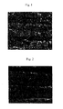
- FIG. 1 is a photomicrograph of the roughened surface of the particle layer formed on the S side of the.electrodeposited copper foil .
- the shinny side (S side) of electrodeposited copper foil 12 ⁇ m thick was plated with a copper-cobalt-nickel alloy under the above-described conditions, so as to form a particle layer about 0.1 to 0.8 ⁇ m thick, the top of which was over-plated with a cobalt-nickel alloy under the above-described conditions (formation of a coating layer).
- FIG. 3 is a photomicrograph of the roughened surface of the particle layer formed on the S side of the electrodeposited copper foil .
- the opening ratios were 100 % under both conditions 1 and 2, which were extremely excellent results.
- a trace quantity of powder drop-off (peel-off and dislodgement of the plated layer) due to a rub was observed, it was not a problem.
- the copper-containing plating which was for forming a particle layer of the present invention, was an effective means for preventing the peel-off and dislodgement of the plated layer.
- the opening ratios were 100 % under both conditions 1 and 2, which were extremely excellent results, like example 1. In this case, no powder drop-off (peel-off and dislodgement of the plated layer) due to a rub was observed.
- Example 2 is a case where cobalt-nickel over-plating was applied after the particle layer of the present invention was formed, and it was confirmed from this example that the over-plating was an effective means for preventing the peel-off and dislodgement of the plated layer.
- Comparative example 1 is a case where the copper foil was used as it was. Although no powder drop-off due to a rub was observed, the laser beam opening ratio was 0 % under the condition 1, that is, a hole could not be made in the copper foil by the laser beam drilling. Under condition 2, the opening ratio was as low as 9 %, which was extremely bad result as well.
- a hole cannot substantially be made in copper foil as it is by the carbon dioxide laser beam drilling.
- a particle layer 0.01 to 3 ⁇ m thick is formed on the surface of copper foil, thereby the hole processability of the copper foil in the laser beam drilling is improved, as shown in the above example.
- the phenomenon of powder drop-off can be prevented effectively by allowing the plating composition for use in the formation of the particle layer to contain copper.
- the use of over-plating makes the prevention more effective, and such means can be adopted according to the situation.
- the present invention allows making a hole directly in copper foil and forming an via-hole in a simple and convenience manner by the low energy laser beam drilling using, for example, carbon dioxide laser beam, in addition, it is remarkably effective in preventing the peel-off and dislodgement of the plated layer caused by a rub.
Landscapes
- Engineering & Computer Science (AREA)
- Manufacturing & Machinery (AREA)
- Microelectronics & Electronic Packaging (AREA)
- Physics & Mathematics (AREA)
- Optics & Photonics (AREA)
- Chemical & Material Sciences (AREA)
- Chemical Kinetics & Catalysis (AREA)
- Electrochemistry (AREA)
- Materials Engineering (AREA)
- Metallurgy (AREA)
- Organic Chemistry (AREA)
- Parts Printed On Printed Circuit Boards (AREA)
- Electroplating Methods And Accessories (AREA)
- Laminated Bodies (AREA)
- Printing Elements For Providing Electric Connections Between Printed Circuits (AREA)
Applications Claiming Priority (3)
| Application Number | Priority Date | Filing Date | Title |
|---|---|---|---|
| JP2000103505 | 2000-04-05 | ||
| JP2000103505A JP3330925B2 (ja) | 2000-04-05 | 2000-04-05 | レーザー穴開け用銅箔 |
| PCT/JP2001/002706 WO2001077420A1 (fr) | 2000-04-05 | 2001-03-30 | Forage de trou par laser dans une tôle de cuivre |
Publications (2)
| Publication Number | Publication Date |
|---|---|
| EP1273682A1 true EP1273682A1 (de) | 2003-01-08 |
| EP1273682A4 EP1273682A4 (de) | 2003-04-16 |
Family
ID=26345056
Family Applications (1)
| Application Number | Title | Priority Date | Filing Date |
|---|---|---|---|
| EP01917661A Withdrawn EP1273682A4 (de) | 2000-04-05 | 2001-03-30 | Kupferfolie mit durch laser erzeugtes loch |
Country Status (3)
| Country | Link |
|---|---|
| EP (1) | EP1273682A4 (de) |
| CN (1) | CN1388841A (de) |
| WO (1) | WO2001077420A1 (de) |
Cited By (2)
| Publication number | Priority date | Publication date | Assignee | Title |
|---|---|---|---|---|
| US10212814B2 (en) | 2012-03-01 | 2019-02-19 | Mitsui Mining & Smelting Co., Ltd. | Copper foil provided with carrier foil, manufacturing method of the copper foil provided with carrier foil, and copper clad laminate for laser drilling manufactured by using the copper foil provided with carrier foil |
| US10639405B2 (en) | 2014-07-22 | 2020-05-05 | Asahi Kasei Medical Co., Ltd. | Adsorbent for removing histone and purification device for liquid derived from living organism |
Families Citing this family (2)
| Publication number | Priority date | Publication date | Assignee | Title |
|---|---|---|---|---|
| US7476449B2 (en) * | 2003-02-27 | 2009-01-13 | Furukawa Circuit Foil Co., Ltd. | Electromagnetic shielding copper foil, method of production thereof and electromagnetic shield |
| CN111850628A (zh) * | 2020-06-12 | 2020-10-30 | 九江德福科技股份有限公司 | 一种屏蔽阴极板的打孔铜箔制作方法 |
Family Cites Families (8)
| Publication number | Priority date | Publication date | Assignee | Title |
|---|---|---|---|---|
| JP2717911B2 (ja) * | 1992-11-19 | 1998-02-25 | 日鉱グールド・フォイル株式会社 | 印刷回路用銅箔及びその製造方法 |
| JP2717910B2 (ja) * | 1992-11-19 | 1998-02-25 | 日鉱グールド・フォイル株式会社 | 印刷回路用銅箔及びその製造方法 |
| JP2762386B2 (ja) * | 1993-03-19 | 1998-06-04 | 三井金属鉱業株式会社 | 銅張り積層板およびプリント配線板 |
| US5482784A (en) * | 1993-12-24 | 1996-01-09 | Mitsui Mining And Smelting Co., Ltd. | Printed circuit inner-layer copper foil and process for producing the same |
| JP3367805B2 (ja) * | 1995-09-28 | 2003-01-20 | 株式会社日鉱マテリアルズ | 印刷回路用銅箔の処理方法 |
| JP3295308B2 (ja) * | 1996-06-28 | 2002-06-24 | 株式会社日鉱マテリアルズ | 電解銅箔 |
| JP3612594B2 (ja) * | 1998-05-29 | 2005-01-19 | 三井金属鉱業株式会社 | 樹脂付複合箔およびその製造方法並びに該複合箔を用いた多層銅張り積層板および多層プリント配線板の製造方法 |
| EP0996318B1 (de) * | 1998-10-19 | 2006-04-19 | Mitsui Mining & Smelting Co., Ltd. | Neue Verbundfolie, Verfahren zu deren Herstellung und Kupferkaschiertes Laminat |
-
2001
- 2001-03-30 WO PCT/JP2001/002706 patent/WO2001077420A1/ja not_active Ceased
- 2001-03-30 EP EP01917661A patent/EP1273682A4/de not_active Withdrawn
- 2001-03-30 CN CN01802679A patent/CN1388841A/zh active Pending
Cited By (2)
| Publication number | Priority date | Publication date | Assignee | Title |
|---|---|---|---|---|
| US10212814B2 (en) | 2012-03-01 | 2019-02-19 | Mitsui Mining & Smelting Co., Ltd. | Copper foil provided with carrier foil, manufacturing method of the copper foil provided with carrier foil, and copper clad laminate for laser drilling manufactured by using the copper foil provided with carrier foil |
| US10639405B2 (en) | 2014-07-22 | 2020-05-05 | Asahi Kasei Medical Co., Ltd. | Adsorbent for removing histone and purification device for liquid derived from living organism |
Also Published As
| Publication number | Publication date |
|---|---|
| WO2001077420A1 (fr) | 2001-10-18 |
| CN1388841A (zh) | 2003-01-01 |
| EP1273682A4 (de) | 2003-04-16 |
Similar Documents
| Publication | Publication Date | Title |
|---|---|---|
| US20020182432A1 (en) | Laser hole drilling copper foil | |
| US6833198B2 (en) | Copper clad laminate | |
| CN102224281B (zh) | 印刷电路用铜箔 | |
| KR101853519B1 (ko) | 액정 폴리머 구리 피복 적층판 및 당해 적층판에 사용하는 구리박 | |
| EP1276358B1 (de) | Verfahren zur herstellung einer kupferfolie mit ausgezeichneten laserstrahl-bohr-eigenschaften | |
| CN101695215B (zh) | 具有低断面的结合增强的铜箔 | |
| JPH06169169A (ja) | 印刷回路用銅箔及びその製造方法 | |
| KR20070064282A (ko) | 캐리어 부착 극박 동박 및 프린트 배선 기판 | |
| US6548153B2 (en) | Composite material used in making printed wiring boards | |
| JP3295308B2 (ja) | 電解銅箔 | |
| KR101451489B1 (ko) | 전자 회로 및 그 형성 방법 그리고 전자 회로 형성용 동장 적층판 | |
| CN103958743B (zh) | 印刷电路用铜箔 | |
| JP3330925B2 (ja) | レーザー穴開け用銅箔 | |
| CN1076154C (zh) | 铜箔及采用该铜箔制作内层电路的高密度多层印刷电路板 | |
| KR101992507B1 (ko) | 전해 구리 합금박 및 캐리어박 부착 전해 구리 합금박 | |
| TWI590719B (zh) | Printed circuit copper foil | |
| JPH06169168A (ja) | 印刷回路用銅箔及びその製造方法 | |
| CA2070046A1 (en) | Metal foil with improved bonding to substrates and method for making said foil | |
| EP0996318B1 (de) | Neue Verbundfolie, Verfahren zu deren Herstellung und Kupferkaschiertes Laminat | |
| JP3615973B2 (ja) | 新規な複合箔およびその製造方法、銅張り積層板 | |
| JP2005240132A (ja) | 電解銅箔及び電解銅箔光沢面の電解研磨方法 | |
| JPH06237078A (ja) | 印刷回路用銅箔の製造方法 | |
| JP3785022B2 (ja) | レーザー穴開け性に優れた樹脂積層板 | |
| JPH06169170A (ja) | 印刷回路用銅箔及びその製造方法 | |
| HK1025463A (en) | A composite material for use in making printed wiring boards |
Legal Events
| Date | Code | Title | Description |
|---|---|---|---|
| PUAI | Public reference made under article 153(3) epc to a published international application that has entered the european phase |
Free format text: ORIGINAL CODE: 0009012 |
|
| 17P | Request for examination filed |
Effective date: 20020123 |
|
| AK | Designated contracting states |
Kind code of ref document: A1 Designated state(s): AT BE CH CY DE DK ES FI FR GB GR IE IT LI LU MC NL PT SE TR |
|
| A4 | Supplementary search report drawn up and despatched |
Effective date: 20030228 |
|
| RIC1 | Information provided on ipc code assigned before grant |
Ipc: 7H 05K 3/00 B Ipc: 7C 25D 7/06 A |
|
| 17Q | First examination report despatched |
Effective date: 20030730 |
|
| RBV | Designated contracting states (corrected) |
Designated state(s): DE FR GB LU |
|
| STAA | Information on the status of an ep patent application or granted ep patent |
Free format text: STATUS: THE APPLICATION IS DEEMED TO BE WITHDRAWN |
|
| 18D | Application deemed to be withdrawn |
Effective date: 20040716 |