EP1274105A1 - Procédé et dispositif d'equilibrage de supercapacité - Google Patents
Procédé et dispositif d'equilibrage de supercapacité Download PDFInfo
- Publication number
- EP1274105A1 EP1274105A1 EP02291430A EP02291430A EP1274105A1 EP 1274105 A1 EP1274105 A1 EP 1274105A1 EP 02291430 A EP02291430 A EP 02291430A EP 02291430 A EP02291430 A EP 02291430A EP 1274105 A1 EP1274105 A1 EP 1274105A1
- Authority
- EP
- European Patent Office
- Prior art keywords
- voltage
- supercapacitor
- terminals
- called
- supercapacitors
- Prior art date
- Legal status (The legal status is an assumption and is not a legal conclusion. Google has not performed a legal analysis and makes no representation as to the accuracy of the status listed.)
- Granted
Links
Images


Classifications
-
- H—ELECTRICITY
- H02—GENERATION; CONVERSION OR DISTRIBUTION OF ELECTRIC POWER
- H02J—ELECTRIC POWER NETWORKS; CIRCUIT ARRANGEMENTS OR SYSTEMS FOR SUPPLYING OR DISTRIBUTING ELECTRIC POWER; SYSTEMS FOR STORING ELECTRIC ENERGY
- H02J7/00—Circuit arrangements for charging or discharging batteries or for supplying loads from batteries
- H02J7/50—Circuit arrangements for charging or discharging batteries or for supplying loads from batteries acting upon multiple batteries simultaneously or sequentially
- H02J7/52—Circuit arrangements for charging or discharging batteries or for supplying loads from batteries acting upon multiple batteries simultaneously or sequentially for charge balancing, e.g. equalisation of charge between batteries
- H02J7/54—Passive balancing, e.g. using resistors or parallel MOSFETs
-
- H—ELECTRICITY
- H02—GENERATION; CONVERSION OR DISTRIBUTION OF ELECTRIC POWER
- H02H—EMERGENCY PROTECTIVE CIRCUIT ARRANGEMENTS
- H02H7/00—Emergency protective circuit arrangements specially adapted for specific types of electric machines or apparatus or for sectionalised protection of cable or line systems, and effecting automatic switching in the event of an undesired change from normal working conditions
- H02H7/16—Emergency protective circuit arrangements specially adapted for specific types of electric machines or apparatus or for sectionalised protection of cable or line systems, and effecting automatic switching in the event of an undesired change from normal working conditions for capacitors
-
- Y—GENERAL TAGGING OF NEW TECHNOLOGICAL DEVELOPMENTS; GENERAL TAGGING OF CROSS-SECTIONAL TECHNOLOGIES SPANNING OVER SEVERAL SECTIONS OF THE IPC; TECHNICAL SUBJECTS COVERED BY FORMER USPC CROSS-REFERENCE ART COLLECTIONS [XRACs] AND DIGESTS
- Y02—TECHNOLOGIES OR APPLICATIONS FOR MITIGATION OR ADAPTATION AGAINST CLIMATE CHANGE
- Y02T—CLIMATE CHANGE MITIGATION TECHNOLOGIES RELATED TO TRANSPORTATION
- Y02T10/00—Road transport of goods or passengers
- Y02T10/60—Other road transportation technologies with climate change mitigation effect
- Y02T10/70—Energy storage systems for electromobility, e.g. batteries
Definitions
- the present invention relates to a charging method and system.
- at least one supercapacitor i.e. one or more supercapacitors, more particularly suitable for balancing supercapacitors.
- Supercapacitors are known devices and are being developed. development at present as sources of energy in high power applications such as in particular the starting of engines, the additional power of hybrid vehicle engines, uninterruptible power supplies. In this type of applications, it is necessary to have sources of energy capable of recharging quickly and to carry out very many cycles, which is the case with supercapacitors unlike traditional batteries.
- Supercapacitors are capable of delivering power very important specifics over short periods. Indeed, the duration of discharge (or charge) characteristic of a supercapacitor is of the order of a few seconds to a few tens of seconds, duration during which specific powers greater than kW / kg can be delivered.
- the supercapacitors have individual capacities with values ranging from Farad at around 3500 F, and very low resistances, less than m ⁇ for the elements of higher capacity.
- document EP-0 564 149 proposes to connect in parallel to the terminals of each supercapacitor of a module several supercapacitors, a branch circuit, known as a bypass circuit, including a MOS transistor which will switch from a voltage predefined across the supercapacitor and derive a current at a intensity, called nominal bypass intensity.
- this guy branch circuit involves the use of a charge current equal to nominal bypass current at end of charge. Indeed, if we continue the charge of a supercapacitor at a much higher intensity than nominal bypass current, overcapacity risks overload resulting in a decrease in its lifespan. Consequently, the use of a low charge current equal to the nominal bypass current going very widely increase the end of charge time.
- the present invention aims to provide a method of charging supercapacitor to continue charging the supercapacitor at a higher current than the nominal bypass current when the bypass started to divert the current and thereby decrease the time of end of charge.
- the present invention provides for this purpose a method of charging at least minus a supercapacitor including an intensity derivation step circulating in said supercapacitor such that when the voltage across the terminals of said supercapacitor reaches a predetermined value, called threshold voltage, the shunt current takes a maximum value called nominal current of bypass, said method being characterized in that it comprises a step of control of the charge intensity of said supercapacitor as a function of the voltage across the supercapacitor by a logic detection function voltage, called optimization function, capable of passing from a so-called state activated at a state called deactivated when the voltage across said terminals supercapacitor exceeds a first predefined voltage greater than the threshold voltage then return to the activated state when the terminal voltage of said supercapacity becomes less than a second predefined voltage less than or equal to said first predefined voltage.
- a logic detection function voltage called optimization function
- the invention it is possible to continue to charge the supercapacitor to an intensity greater than the nominal bypass intensity when the bypass occurred and control the charge intensity as a function of the voltage across the supercapacitor without risk of overshooting a voltage predefined may lead to a reduction in service life.
- the process according to the invention therefore makes it possible to optimize the charging time without deteriorating supercapacitor.
- the signal delivered by said optimization function is a signal in the form of hysteresis.
- the method includes a step of charge of said supercapacitor with a charge intensity greater than said nominal bypass current and maintaining this step of load as long as said optimization function is in the activated state.
- the bypass intensity takes a value much lower than the intensity of the leakage current of said supercapacitor.
- the characteristic of the bypass current in function of the voltage across the supercapacitor is a signal in the form hysteresis.
- the all or nothing characteristic of the bypass current as a function of the voltage across the supercapacitor therefore has a form of hysteresis and improves stability when the voltage of the supercapacitor due, for example, to a sudden change in the current of charge.
- the method includes a step of filtering of high frequency harmonics of the voltage across the supercapacitor.
- the use of a low-pass filter makes it possible to filter high frequency harmonics of the voltage across the supercapacitor induced by high frequency cutting of the charging current.
- the method includes a step of reset the charger according to the voltage across the supercapacitor by a logic voltage detection function, called function reset, likely to go from a so-called activated state to a so-called state deactivated when the voltage across said supercapacitor exceeds one third predefined voltage less than or equal to said first voltage predefined then return to the so-called activated state when said terminal voltage of said supercapacity becomes less than a fourth predefined voltage lower than said second predefined voltage.
- function reset a logic voltage detection function
- the method includes a step of detecting minimum safety voltage across the supercapacitor by a function voltage detection logic, called voltage detection function minimal, likely to go from a so-called activated state to a so-called deactivated state when the voltage across said supercapacitor exceeds one fifth preset voltage then return to the so-called activated state when said voltage at terminals of said supercapacity becomes less than a sixth voltage predefined.
- a function voltage detection logic called voltage detection function minimal
- the charging method includes a step of charge of a plurality of supercapacitors characterized in that said function optimization goes from a so-called activated state to a so-called deactivated state when one at least voltages across said supercapacitors exceeds said first preset voltage and returns to the activated state when each of the voltages across said supercapacitors becomes lower than said second preset voltage.
- the charging method comprising a charging step of a plurality of supercapacitors is characterized in that said reset function changes from a so-called activated state to a so-called state deactivated when at least one of the voltages across said terminals supercapacitors exceeds said third predefined voltage and returns to the state said activated when each of the voltages across said supercapacitors becomes lower than said fourth predefined voltage.
- the charging method comprising a step of charge of a plurality of supercapacitors is characterized in that said minimum voltage detection function changes from a so-called activated state to a state said deactivated when each of the voltages across said supercapacitors exceeds said fifth predefined voltage and returns to the so-called activated state when at least one of the voltages across said supercapacitors becomes lower than said sixth predefined voltage.
- the charging method comprising a step of charging a plurality of supercapacitors includes a step of detecting dispersion of the voltage across said supercapacitors by a function voltage detection logic, called dispersion detection function, characterized in that said dispersion detection function changes from a said active state to a so-called deactivated state when each of the terminal voltages said supercapacitors exceeds a predefined seventh voltage and returns to the state called activated when at least one of the voltages across said terminals supercapacitors becomes less than a predefined eighth voltage.
- a function voltage detection logic called dispersion detection function
- the combination of the end of charge optimization function and this dispersion detection function detects an imbalance large voltages across the supercapacitors in a module supercapacitors.
- the system includes a low pass filter mounted in parallel at the terminals of said supercapacitor.
- the system comprises a plurality of supercapacitors connected in series, a branch circuit being mounted in parallel with the terminals of each of said supercapacitors.
- the system comprises a plurality of supercapacitors connected in series, a single branch circuit being mounted in parallel across all of said supercapacitors.
- the system comprises a plurality of supercapacitors mounted in parallel, a branch circuit single being mounted in parallel across all of said supercapacitors.
- a charging system 10 comprising a supercapacitor 11 at the terminals of which is mounted in parallel a circuit 12 called bypass in which flows a bypass current I BP , the circuit 12 comprising a MOS transistor switching power.
- a low-pass filter 13 is mounted in parallel at the terminals of the supercapacitor 11. This low-pass filter 13 is made necessary in the event of high frequency cutting of the load current I C generating voltage harmonics detrimental to the proper functioning of the circuit. bypass 12.
- a detection member 14 connected to the filter 13 generates two logical charge management functions F 0 and F 1 , respectively called optimization function and reset function, including the interpretation by the charger 15 of the supercapacitor 11 allows in particular to optimize the charging time without deteriorating the supercapacitor and to reset the charger.
- the filter 13 generates a filtered voltage V representative of the voltage across the supercapacitors 11 without voltage harmonics. The voltage V controls the circuit 12 and the member 14.
- FIG. 2 shows a system 20 for charging a supercapacitor module comprising a plurality (6 in the example of FIG. 2) of circuits 10 1 to 10 6 such as that of FIG. 1.
- Each element of a circuit 10 n (n varying from 1 to 6 in the example in FIG. 2) comprises the same elements as the circuit 10 in FIG. 1, referenced with the same number bearing the index corresponding to the rank of this circuit in the module 20
- the charger 15 and the detection member 14 are common to all the supercapacitors 11 1 to 11 6 .
- the output voltages V i of each circuit are combined in the detection member 14 to generate the logic functions F 0 and F 1 , the two logic functions being sent to the charger 15.
- FIG. 3 shows an example of a characteristic curve of the shunt intensity, denoted I BP , and of the optimization function F 0 according to the method of the invention as a function of the voltage V across the terminals of the supercapacitor.
- Curve 21 in solid lines represents the optimization function F 0 as a function of the voltage V across the terminals of the supercapacitor.
- Curve 22 in dotted lines represents the bypass intensity I BP as a function of the voltage V across the supercapacitors.
- Figure 3 has been described above with reference to Figure 1.
- the optimization function F 0 passes from a activated state to a deactivated state when at least one of the voltages at the terminals of the supercapacitors exceeds the first predefined voltage V 0H and returns to the activated state when each of the voltages V 1 to V 6 at the terminals of said supercapacitors becomes lower than said second preset voltage V 0B .
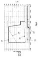
- FIG. 4 shows an example of a curve representing the voltage V T at the terminals of a module of six supercapacitors as shown in FIG. 2, the intensity I C of charge of the supercapacitors module, the voltage V 6 at the terminals of the supercapacitor 11 6 , the bypass intensity I BP corresponding to the circuit 10 6 and the optimization function F 0 as a function of the charging time using a method according to the invention.
- the curve 25 in dotted lines represents the voltage V T at the terminals of the supercapacitors module as a function of the charging time.
- the curve 23 in thick solid lines represents the intensity I C of charge of the supercapacitors module as a function of the charge time.
- the curve 24 in solid lines represents the voltage V 6 at the terminals of the supercapacitor 11 6 as a function of the charging time.
- the curve 27 in solid lines represents the bypass intensity I BP corresponding to the circuit 10 6 as a function of the charging time.
- Curve 26 in thick dotted lines represents the optimization function F 0 as a function of the charging time.
- the charging current I C is constant and equal to approximately 200 A.
- the supercapacitor 11 6 is charged, which implies the gradual increase in the voltage V 6 and in the overall voltage V T.
- the function F 0 is in the activated state.
- the shunt intensity is close to zero or in any case much lower than the leakage current of the supercapacitors.
- the function F 0 being always at l state activated, it indicates to the charger 15 that it can maintain a charging current at 200 A.
- the supercapacitors charge again at an intensity equal to approximately 55 A. This phase again involves an increase in V 6 and V T.
- F 0 returns to the deactivated state and indicates to the charger 15 that the latter must reduce the charge intensity which passes to a value close to zero.
- the charging protocol as described above makes it possible to continue charging the supercapacitor at an intensity greater than the nominal bypass intensity equal to 1A when the bypass has taken place and to control the charge intensity as a function of the auxiliary voltage.
- supercapacitor limits thanks to the value of the logic function F 0 which controls the charger, without the risk of exceeding a predefined voltage which could lead to a reduction in the life of the supercapacitor.
- the charger reset function F 1 is capable of passing from an activated state to a deactivated state when the voltage V across the supercapacitor 11 exceeds a third predefined voltage less than or equal to the first predefined voltage V 0H and then return to the activated state when the voltage V across the supercapacitor 11 becomes less than a fourth predefined voltage less than said second predefined voltage V 0B .
- the optimization function F 1 changes from an activated state to a deactivated state when at least one of the voltages V 1 to V 6 at the terminals of the supercapacitors 11 1 to 11 6 exceeds the third predefined voltage and returns to the activated state when each of the voltages V 1 to V 6 at the terminals of said supercapacitors 11 1 to 11 6 becomes lower than the fourth predefined voltage .
- the characteristic of the charge intensity such that described above has a ramp-shaped part but it is fine obvious that it can be quite different, for example in the shape of a staircase using several constant levels of current as a function of time.
- MOS transistor for the branch circuit but it is understood that any type of transistor such as an IGBT transistor operating in switching mode can be used.
- the invention in all of its embodiments, applies both at the expense of a supercapacitor alone and at the expense of a module of several supercapacitors.
Landscapes
- Engineering & Computer Science (AREA)
- Power Engineering (AREA)
- Charge And Discharge Circuits For Batteries Or The Like (AREA)
- Secondary Cells (AREA)
Abstract
Description
- au moins une supercapacité
- un circuit de dérivation comprenant un transistor fonctionnant en commutation et monté en parallèle aux bornes de ladite supercapacité,
- des moyens de charge,
- un organe de détection délivrant au moins un signal logique représentatif de la tension aux bornes de ladite supercapacité, ledit signal logique étant fourni aux dits moyens de charge.
- La figure 1 représente le schéma de principe d'un système de charge pour la mise en oeuvre du procédé selon l'invention sur une supercapacité élémentaire,
- La figure 2 représente le schéma de principe d'un système de charge pour la mise en oeuvre du procédé selon l'invention sur un module de plusieurs supercapacités,
- La figure 3 montre un exemple de courbe caractéristique de l'intensité de dérivation et de la fonction d'optimisation selon le procédé de l'invention en fonction de la tension aux bornes de la supercapacité,
- La figure 4 montre un exemple de courbe représentant la tension aux bornes d'un module de supercapacités, l'intensité de charge d'un module de supercapacités, la tension aux bornes d'une des supercapacités du module, l'intensité de dérivation et la fonction d'optimisation en fonction du temps de charge utilisant un procédé selon l'invention.

- Tant que la tension V est inférieure à une tension VS, dite tension de seuil, le courant de dérivation IBP a une intensité très inférieure au courant de fuite de la supercapacité 11.
- Dès que la tension V atteint la tension VS, le transistor du circuit de dérivation 12 commute et le courant de dérivation IBP prend une valeur déterminée de l'ordre de quelques centaines de milliampères à quelques ampères.
- Quand la tension V rediminue et redevient inférieure à une tension VR, dite tension de référence, l'intensité de dérivation redevient inférieure à l'intensité du courant de fuite de la supercapacité 11.
- Tant que la tension V est inférieure à une première tension prédéfinie, notée V0H, F0 est à l'état activé, c'est à dire que F0 a une valeur de tension égale à quelques volts correspondant au 1 de la logique binaire. V0H est une tension supérieure à la tension de seuil VS.
- Dès que V atteint V0H, F0 prend une valeur quasi nulle et passe donc à un état désactivé correspondant au 0 de la logique binaire.
- Quand V rediminue et redevient inférieure à une deuxième tension prédéfinie, notée V0B, F0 repasse à l'état activé correspondant au 1 de la logique binaire.
Claims (17)
- Procédé de charge d'au moins une supercapacité (11) comprenant une étape (22) de dérivation de l'intensité circulant dans ladite supercapacité telle que, lorsque la tension (V) aux bornes de ladite supercapacité atteint une valeur prédéterminée, dite tension de seuil (VS), l'intensité de dérivation (IBP) prend une valeur maximale dite intensité nominale de dérivation, ledit procédé étant caractérisé en ce qu'il comprend une étape (21) de contrôle de l'intensité de charge (IC) de ladite supercapacité en fonction de la tension (V) aux bornes de ladite supercapacité par une fonction logique (F0) de détection de tension, dite fonction d'optimisation, susceptible de passer d'un état dit activé à un état dit désactivé lorsque la tension (V) aux bornes de ladite supercapacité dépasse une première tension prédéfinie (V0H) supérieure à la tension de seuil (VS) puis de repasser à l'état activé lorsque ladite tension (V) aux bornes de ladite supercapacité devient inférieure à une deuxième tension prédéfinie (V0B) inférieure ou égale à ladite première tension prédéfinie (V0H).
- Procédé de charge selon la revendication 1, dans lequel ledit signal délivré par ladite fonction d'optimisation (F0) est un signal sous forme d'hystérésis.
- Procédé de charge selon l'une des revendications 1 ou 2, comportant une étape de charge de ladite supercapacité avec une intensité de charge (IC) supérieure à ladite intensité nominale de dérivation et un maintien de cette étape de charge tant que ladite fonction logique d'optimisation (F0) est à l'état activé.
- Procédé de charge selon l'une des revendications précédentes, comportant une étape telle que, lorsque la tension (V) aux bornes de ladite supercapacité revient à une valeur de tension, dite tension de référence (VR), qui est inférieure à la valeur de ladite tension de seuil (VS), l'intensité de dérivation (IBP) prend une valeur très inférieure à une intensité correspondant au courant de fuite de ladite supercapacité.
- Procédé de charge selon la revendication précédente, dans lequel la caractéristique du courant de dérivation en fonction de la tension aux bornes de ladite supercapacité est un signal sous forme d'hystérésis.
- Procédé de charge selon l'une des revendications précédentes, comportant une étape de filtrage des harmoniques hautes fréquences de ladite tension (V) aux bornes de ladite supercapacité.
- Procédé de charge selon l'une des revendications précédentes, comportant une étape de réinitialisation du chargeur (15) en fonction de la tension (V) aux bornes de la supercapacité par une fonction logique de détection de tension, dite fonction de réinitialisation (F1), susceptible de passer d'un état dit activé à un état dit désactivé lorsque la tension (V) aux bornes de ladite supercapacité dépasse une troisième tension prédéfinie inférieure ou égale à ladite première tension prédéfinie (V0H) puis de repasser à l'état dit activé lorsque ladite tension (V) aux bornes de ladite supercapacité devient inférieure à une quatrième tension prédéfinie inférieure à ladite deuxième tension prédéfinie (V0B).
- Procédé de charge selon l'une des revendications précédentes, comportant une étape de détection de tension minimale de sécurité aux bornes de la supercapacité par une fonction logique de détection de tension, dite fonction de détection de tension minimale, susceptible de passer d'un état dit activé à un état dit désactivé lorsque la tension aux bornes de ladite supercapacité dépasse une cinqième tension prédéfinie puis de repasser à l'état dit activé lorsque ladite tension aux bornes de ladite supercapacité devient inférieure à une sixième tension prédéfinie.
- Procédé de charge selon l'une des revendications précédentes, comportant une étape de charge d 'une pluralité de supercapacités (11i), dans lequel ladite fonction d'optimisation (F0) passe d'un état dit activé à un état dit désactivé lorsque l'une au moins des tensions (Vi) aux bornes desdites supercapacités dépasse ladite première tension prédéfinie (V0H) et repasse à l'état activé lorsque chacune des tensions (Vi) aux bornes desdites supercapacités devient inférieure à ladite deuxième tension prédéfinie (V0B).
- Procédé de charge selon la revendication 7, dans lequel ladite fonction de réinitialisation (F1) passe d'un état dit activé à un état dit désactivé lorsque l'une au moins des tensions (Vi) aux bornes desdites supercapacités dépasse ladite troisième tension prédéfinie et repasse à l'état dit activé lorsque chacune des tensions (Vi) aux bornes desdites supercapacités devient inférieure à ladite quatrième tension prédéfinie.
- Procédé de charge selon l'une des revendications 9 ou 10, dans lequel ladite fonction de détection de tension minimale passe d'un état dit activé à un état dit désactivé lorsque chacune des tensions (Vi) aux bornes desdites supercapacités dépasse ladite cinquième tension prédéfinie et repasse à l'état dit activé lorsque l'une au moins des tensions (Vi) aux bornes desdites supercapacités devient inférieure à ladite sixième tension prédéfinie.
- Procédé de charge selon l'une des revendications 9 à 11, comportant une étape de détection de dispersion de la tension aux bornes desdites supercapacités par une fonction logique de détection de tension, dite fonction de détection de dispersion, dans lequel ladite fonction de détection de dispersion passe d'un état dit activé à un état dit désactivé lorsque chacune des tensions (Vi) aux bornes desdites supercapacités dépasse une septième tension prédéfinie et repasse à l'état dit activé lorsque l'une au moins des tensions aux bornes desdites supercapacités devient inférieure à une huitième tension prédéfinie.
- Système (10, 20) pour la mise en oeuvre du procédé selon l'une des revendications précédentes, dans lequel ledit système comprend :au moins une supercapacité (11, 11i)un circuit de dérivation (12, 12i) comprenant un transistor fonctionnant en commutation et monté en parallèle aux bornes de ladite supercapacité,des moyens de charge (15),un organe de détection (14) délivrant au moins un signal logique représentatif de la tension aux bornes de ladite supercapacité, ledit signal logique étant fourni aux dits moyens de charge.
- Système (10, 20) selon la revendication précédente, comprenant un filtre passe bas (13, 13i) monté en parallèle aux bornes de ladite supercapacité.
- Système (10, 20) selon l'une des revendications 13 ou 14, comportant une pluralité de supercapacités (11i) montées en série, un circuit de dérivation (12i) étant monté en parallèle aux bornes de chacune desdites supercapacités.
- Système selon l'une des revendications 13 ou 14, comportant une pluralité de supercapacités montées en série, un circuit de dérivation unique étant monté en parallèle aux bornes de l'ensemble desdites supercapacités.
- Système selon l'une des revendications 13 ou 14, comportant une pluralité de supercapacités montées en parallèle, un circuit de dérivation unique étant monté en parallèle aux bornes de l'ensemble desdites supercapacités.
Applications Claiming Priority (4)
| Application Number | Priority Date | Filing Date | Title |
|---|---|---|---|
| FR0107959 | 2001-06-18 | ||
| FR0107959A FR2826202B1 (fr) | 2001-06-18 | 2001-06-18 | Procede et dispositif d'equilibrage de supercapacite |
| FR0206037 | 2002-05-16 | ||
| FR0206037A FR2826203B1 (fr) | 2001-06-18 | 2002-05-16 | Procede et dispositif d'equilibrage de supercapacite |
Publications (2)
| Publication Number | Publication Date |
|---|---|
| EP1274105A1 true EP1274105A1 (fr) | 2003-01-08 |
| EP1274105B1 EP1274105B1 (fr) | 2005-10-05 |
Family
ID=26213054
Family Applications (1)
| Application Number | Title | Priority Date | Filing Date |
|---|---|---|---|
| EP02291430A Expired - Lifetime EP1274105B1 (fr) | 2001-06-18 | 2002-06-10 | Procédé et dispositif d'équilibrage de supercapacité |
Country Status (4)
| Country | Link |
|---|---|
| US (1) | US6777917B2 (fr) |
| EP (1) | EP1274105B1 (fr) |
| DE (1) | DE60206447T2 (fr) |
| FR (1) | FR2826203B1 (fr) |
Cited By (1)
| Publication number | Priority date | Publication date | Assignee | Title |
|---|---|---|---|---|
| WO2011023265A3 (fr) * | 2009-08-27 | 2012-05-10 | Voith Patent Gmbh | Système d'accumulation d'énergie électrique |
Families Citing this family (19)
| Publication number | Priority date | Publication date | Assignee | Title |
|---|---|---|---|---|
| DE10236165B4 (de) * | 2002-08-07 | 2004-08-12 | Siemens Ag | Verfahren und Vorrichtung zum Symmetrieren der Kondensatoren einer Kondensatorbatterie |
| US7275501B1 (en) * | 2003-07-03 | 2007-10-02 | Laceky William P | System and method using capacitors to power an automatic feeder system |
| US8525469B1 (en) | 2003-07-03 | 2013-09-03 | Battery-Free Outdoors, Llc | System and method using capacitors to power a camera having a motion sensor |
| US20060264188A1 (en) * | 2003-08-29 | 2006-11-23 | Pierre Mars | Power supply for a communications module that demands high power during predetermined periods |
| US20070112485A1 (en) * | 2005-11-17 | 2007-05-17 | Snap-On Incorporated | Vehicle service device and system powered by capacitive power source |
| US7918374B2 (en) * | 2007-01-29 | 2011-04-05 | Halex/Scott Fetzer Company | Portable fastener driving device |
| US20090140693A1 (en) * | 2007-11-30 | 2009-06-04 | Eaton Corporation | Flyback charge redistribution apparatus for serially connected energy storage devices using flyback-type converters |
| TWI472120B (zh) * | 2008-07-23 | 2015-02-01 | 皇家飛利浦電子股份有限公司 | 用於對超級電容器充電之方法及充電器 |
| US8269469B2 (en) * | 2008-08-12 | 2012-09-18 | Ivus Industries, Llc | Equalizing method and circuit for ultracapacitors |
| US8598852B2 (en) * | 2008-11-12 | 2013-12-03 | American Axle & Manufacturing, Inc. | Cost effective configuration for supercapacitors for HEV |
| US9312705B2 (en) | 2010-12-22 | 2016-04-12 | Ge Energy Power Conversion Technology Limited | Capacitor balancing circuit and control method for an electronic device such as a multilevel power inverter |
| EP2656496B1 (fr) | 2010-12-22 | 2019-09-11 | GE Energy Power Conversion Technology Limited | Agencement mécanique de circuit convertisseur de puissance à plusieurs niveaux |
| US8742729B2 (en) * | 2011-06-07 | 2014-06-03 | Flashsilicon Incorporation | Rechargeable battery |
| RU2543506C2 (ru) * | 2013-03-11 | 2015-03-10 | Открытое акционерное общество Воронежское специальное конструкторское бюро "Рикон" (ОАО ВСКБ "Рикон") | Устройство электрическое суперконденсаторное |
| US20140266067A1 (en) * | 2013-03-15 | 2014-09-18 | Zvi Kurtzman | Electrical Extension |
| FR3059167B1 (fr) * | 2016-11-18 | 2018-12-07 | Blue Solutions | Systeme d'equilibrage local analogique pour un ensemble de dispositifs de stockage d'energie electrique par effet capacitif, module de stockage rechargeable, vehicule de transport et installation electriques comprenant un tel systeme. |
| US20230361581A1 (en) * | 2020-09-17 | 2023-11-09 | Ucap Power, Inc. | Integrated control and monitoring of ultracapacitor charging and cell balancing |
| DE102021200924B4 (de) | 2021-02-02 | 2025-05-28 | SWJ Germany GmbH | Schaltungsanordnung mit zumindest einem Superkondensator und wenigstens einer Bypass-Schaltung, elektrischer Energiespeicher mit einer Schaltungsanordnung und Verwendung einer Schaltungsanordnung als Energiespeicher |
| DE102022110861B3 (de) | 2022-05-03 | 2023-08-03 | SWJ Germany GmbH | Schaltungsanordnung, elektrischer Energiespeicher, Verwendung einer Schaltungsanordnung und Verfahren zum Betreiben einer Schaltungsanordnung |
Citations (5)
| Publication number | Priority date | Publication date | Assignee | Title |
|---|---|---|---|---|
| US5063340A (en) * | 1990-10-25 | 1991-11-05 | Motorola, Inc. | Capacitive power supply having charge equalization circuit |
| US5528121A (en) * | 1993-05-28 | 1996-06-18 | Jeol Ltd. | Storage capacitor power supply |
| US5545933A (en) * | 1993-09-28 | 1996-08-13 | Okamura Laboratory Inc. | Electric power storage apparatus |
| US5726552A (en) * | 1995-02-27 | 1998-03-10 | Jeol Ltd. | Method and apparatus for controlling charging of electrical power storage unit |
| EP0851445A2 (fr) * | 1996-12-20 | 1998-07-01 | Asahi Glass Company Ltd. | Condensateur électrique à double couche et dispositif d'alimentation de puissance à cellules assemblées |
Family Cites Families (2)
| Publication number | Priority date | Publication date | Assignee | Title |
|---|---|---|---|---|
| US5642027A (en) * | 1992-01-07 | 1997-06-24 | Windes; John A. | Current-limited system for capacitive load powering |
| JPH10191574A (ja) * | 1996-12-26 | 1998-07-21 | Japan Tobacco Inc | 充電装置 |
-
2002
- 2002-05-16 FR FR0206037A patent/FR2826203B1/fr not_active Expired - Fee Related
- 2002-06-10 EP EP02291430A patent/EP1274105B1/fr not_active Expired - Lifetime
- 2002-06-10 DE DE60206447T patent/DE60206447T2/de not_active Expired - Lifetime
- 2002-06-17 US US10/171,970 patent/US6777917B2/en not_active Expired - Fee Related
Patent Citations (5)
| Publication number | Priority date | Publication date | Assignee | Title |
|---|---|---|---|---|
| US5063340A (en) * | 1990-10-25 | 1991-11-05 | Motorola, Inc. | Capacitive power supply having charge equalization circuit |
| US5528121A (en) * | 1993-05-28 | 1996-06-18 | Jeol Ltd. | Storage capacitor power supply |
| US5545933A (en) * | 1993-09-28 | 1996-08-13 | Okamura Laboratory Inc. | Electric power storage apparatus |
| US5726552A (en) * | 1995-02-27 | 1998-03-10 | Jeol Ltd. | Method and apparatus for controlling charging of electrical power storage unit |
| EP0851445A2 (fr) * | 1996-12-20 | 1998-07-01 | Asahi Glass Company Ltd. | Condensateur électrique à double couche et dispositif d'alimentation de puissance à cellules assemblées |
Non-Patent Citations (1)
| Title |
|---|
| BONERT R ET AL: "SUPER-CAPACITORS FOR PEAK LOAD SHAVING OF BATTERIES", EPE '97. 7TH. EUROPEAN CONFERENCE ON POWER ELECTRONICS AND APPLICATIONS. TRONDHEIM, SEPT. 8 - 10, 1997, EPE. EUROPEAN CONFERENCE ON POWER ELECTRONICS AND APPLICATIONS, BRUSSELS, EPE ASSOCIATION, B, vol. 1 CONF. 7, 8 September 1997 (1997-09-08), pages 1055 - 1060, XP000769079, ISBN: 90-75815-02-6 * |
Cited By (1)
| Publication number | Priority date | Publication date | Assignee | Title |
|---|---|---|---|---|
| WO2011023265A3 (fr) * | 2009-08-27 | 2012-05-10 | Voith Patent Gmbh | Système d'accumulation d'énergie électrique |
Also Published As
| Publication number | Publication date |
|---|---|
| FR2826203B1 (fr) | 2003-12-19 |
| DE60206447D1 (de) | 2006-02-16 |
| DE60206447T2 (de) | 2006-05-18 |
| US6777917B2 (en) | 2004-08-17 |
| EP1274105B1 (fr) | 2005-10-05 |
| US20030020435A1 (en) | 2003-01-30 |
| FR2826203A1 (fr) | 2002-12-20 |
Similar Documents
| Publication | Publication Date | Title |
|---|---|---|
| EP1274105B1 (fr) | Procédé et dispositif d'équilibrage de supercapacité | |
| EP1274106B1 (fr) | Procédé et dispositif d'équilibrage de supercapacité | |
| EP3105845B1 (fr) | Systeme d'alimentation a tension continue configure pour precharger un condensateur de filtrage avant l'alimentation d'une charge | |
| EP1790071B1 (fr) | Module de commande et de puissance pour une machine electrique tournante | |
| EP2707945B1 (fr) | Procede de commande d'une machine electrique tournante, systeme de commande et machine electrique tournante correspondants | |
| EP0847124B1 (fr) | Alimentation de secours destinée à suppléer provisoirement à une carence d'une source d'alimentation principale | |
| EP3044025B1 (fr) | Dispositif de détection d'un défaut d'isolement destiné à tester un défaut d'isolement en conditions critiques | |
| EP1383222B1 (fr) | Chargeur pour batterie | |
| EP1848090A2 (fr) | Dispositif de suralimentation temporaire en puissance d'organes électriques | |
| EP3883105A1 (fr) | Dispositif de décharge d'une capacité | |
| FR2721474A1 (fr) | Dispositif de commande d'une lampe fluorescente à basse pression. | |
| FR2751145A1 (fr) | Dispositif de controle de la charge d'un supercondensateur et procede de commande d'un tel dispositif | |
| FR2911732A1 (fr) | Dispositif d'elevation temporaire de tension electrique pour organe automobile | |
| WO2007080349A1 (fr) | Dispositif d'alimentation de l'inducteur d'une machine electrique tournante | |
| EP4434153A1 (fr) | Procédé de protection contre une surtension dans un système comportant une batterie, un onduleur et une machine électrique | |
| EP4639705A1 (fr) | Installation solaire à panneau photovoltaïque | |
| EP0789439A1 (fr) | Dispositif régulateur de la tension de charge d'une batterie par un alternateur, en fonction d'une tension de référence et de la vitesse de rotation de l'alternateur | |
| FR2790341A1 (fr) | Alternateur equipe de moyens perfectionnes de protection contre le delestage de charges, et dispositif regulateur associe | |
| EP4387079A1 (fr) | Système de commande d'un convertisseur de tension | |
| FR3131383A1 (fr) | Système de contrôle d’une pluralité de cellules de batterie et batterie associée | |
| FR3159864A1 (fr) | Systeme electrique pour precharger une capacite agencee entre des lignes positive et negative connectables a une batterie | |
| WO2011121238A2 (fr) | Circuit électrique pour véhicule automobile muni d'un redresseur autonome | |
| FR3098060A1 (fr) | Système électrique et méthode de protection d’un convertisseur DC/DC | |
| EP3425800A1 (fr) | Dispositif de commutation pour transistor sic ou gan mosfet avec circuit de protection contre les surtensions et procédé associé | |
| FR2634960A1 (fr) | Systeme de protection du pont redresseur d'un alternateur de vehicule automobile contre la surtension de delestage de charge |
Legal Events
| Date | Code | Title | Description |
|---|---|---|---|
| PUAI | Public reference made under article 153(3) epc to a published international application that has entered the european phase |
Free format text: ORIGINAL CODE: 0009012 |
|
| AK | Designated contracting states |
Kind code of ref document: A1 Designated state(s): AT BE CH CY DE DK ES FI FR GB GR IE IT LI LU MC NL PT SE TR |
|
| AX | Request for extension of the european patent |
Free format text: AL;LT;LV;MK;RO;SI |
|
| 17P | Request for examination filed |
Effective date: 20030708 |
|
| AKX | Designation fees paid |
Designated state(s): DE FR GB |
|
| GRAP | Despatch of communication of intention to grant a patent |
Free format text: ORIGINAL CODE: EPIDOSNIGR1 |
|
| RAP1 | Party data changed (applicant data changed or rights of an application transferred) |
Owner name: SAFT FINANCE S.AE.R.L. |
|
| RIN1 | Information on inventor provided before grant (corrected) |
Inventor name: SHARIF, FADI Inventor name: RAEL, STEPHANE Inventor name: BARRAILH, GERARD Inventor name: LAVOUR, PASCAL Inventor name: DAVAT, BERNARD Inventor name: DESPREZ, PHILIPPE |
|
| GRAS | Grant fee paid |
Free format text: ORIGINAL CODE: EPIDOSNIGR3 |
|
| GRAA | (expected) grant |
Free format text: ORIGINAL CODE: 0009210 |
|
| AK | Designated contracting states |
Kind code of ref document: B1 Designated state(s): DE FR GB |
|
| REG | Reference to a national code |
Ref country code: GB Ref legal event code: FG4D Free format text: NOT ENGLISH |
|
| GBT | Gb: translation of ep patent filed (gb section 77(6)(a)/1977) |
Effective date: 20051109 |
|
| REF | Corresponds to: |
Ref document number: 60206447 Country of ref document: DE Date of ref document: 20060216 Kind code of ref document: P |
|
| PLBE | No opposition filed within time limit |
Free format text: ORIGINAL CODE: 0009261 |
|
| STAA | Information on the status of an ep patent application or granted ep patent |
Free format text: STATUS: NO OPPOSITION FILED WITHIN TIME LIMIT |
|
| 26N | No opposition filed |
Effective date: 20060706 |
|
| PGFP | Annual fee paid to national office [announced via postgrant information from national office to epo] |
Ref country code: DE Payment date: 20120524 Year of fee payment: 11 |
|
| PGFP | Annual fee paid to national office [announced via postgrant information from national office to epo] |
Ref country code: FR Payment date: 20120625 Year of fee payment: 11 Ref country code: GB Payment date: 20120525 Year of fee payment: 11 |
|
| GBPC | Gb: european patent ceased through non-payment of renewal fee |
Effective date: 20130610 |
|
| REG | Reference to a national code |
Ref country code: FR Ref legal event code: ST Effective date: 20140228 |
|
| REG | Reference to a national code |
Ref country code: DE Ref legal event code: R119 Ref document number: 60206447 Country of ref document: DE Effective date: 20140101 |
|
| PG25 | Lapsed in a contracting state [announced via postgrant information from national office to epo] |
Ref country code: GB Free format text: LAPSE BECAUSE OF NON-PAYMENT OF DUE FEES Effective date: 20130610 Ref country code: DE Free format text: LAPSE BECAUSE OF NON-PAYMENT OF DUE FEES Effective date: 20140101 |
|
| PG25 | Lapsed in a contracting state [announced via postgrant information from national office to epo] |
Ref country code: FR Free format text: LAPSE BECAUSE OF NON-PAYMENT OF DUE FEES Effective date: 20130701 |