EP1274106B1 - Ausgleichsverfahren und -vorrichtung für einen Superkondensator - Google Patents
Ausgleichsverfahren und -vorrichtung für einen Superkondensator Download PDFInfo
- Publication number
- EP1274106B1 EP1274106B1 EP02291431A EP02291431A EP1274106B1 EP 1274106 B1 EP1274106 B1 EP 1274106B1 EP 02291431 A EP02291431 A EP 02291431A EP 02291431 A EP02291431 A EP 02291431A EP 1274106 B1 EP1274106 B1 EP 1274106B1
- Authority
- EP
- European Patent Office
- Prior art keywords
- voltage
- current
- supercapacitor
- bypass
- terminals
- Prior art date
- Legal status (The legal status is an assumption and is not a legal conclusion. Google has not performed a legal analysis and makes no representation as to the accuracy of the status listed.)
- Expired - Lifetime
Links
Images


Classifications
-
- H—ELECTRICITY
- H02—GENERATION; CONVERSION OR DISTRIBUTION OF ELECTRIC POWER
- H02J—ELECTRIC POWER NETWORKS; CIRCUIT ARRANGEMENTS OR SYSTEMS FOR SUPPLYING OR DISTRIBUTING ELECTRIC POWER; SYSTEMS FOR STORING ELECTRIC ENERGY
- H02J7/00—Circuit arrangements for charging or discharging batteries or for supplying loads from batteries
- H02J7/50—Circuit arrangements for charging or discharging batteries or for supplying loads from batteries acting upon multiple batteries simultaneously or sequentially
- H02J7/52—Circuit arrangements for charging or discharging batteries or for supplying loads from batteries acting upon multiple batteries simultaneously or sequentially for charge balancing, e.g. equalisation of charge between batteries
- H02J7/54—Passive balancing, e.g. using resistors or parallel MOSFETs
-
- H—ELECTRICITY
- H02—GENERATION; CONVERSION OR DISTRIBUTION OF ELECTRIC POWER
- H02H—EMERGENCY PROTECTIVE CIRCUIT ARRANGEMENTS
- H02H7/00—Emergency protective circuit arrangements specially adapted for specific types of electric machines or apparatus or for sectionalised protection of cable or line systems, and effecting automatic switching in the event of an undesired change from normal working conditions
- H02H7/16—Emergency protective circuit arrangements specially adapted for specific types of electric machines or apparatus or for sectionalised protection of cable or line systems, and effecting automatic switching in the event of an undesired change from normal working conditions for capacitors
-
- Y—GENERAL TAGGING OF NEW TECHNOLOGICAL DEVELOPMENTS; GENERAL TAGGING OF CROSS-SECTIONAL TECHNOLOGIES SPANNING OVER SEVERAL SECTIONS OF THE IPC; TECHNICAL SUBJECTS COVERED BY FORMER USPC CROSS-REFERENCE ART COLLECTIONS [XRACs] AND DIGESTS
- Y02—TECHNOLOGIES OR APPLICATIONS FOR MITIGATION OR ADAPTATION AGAINST CLIMATE CHANGE
- Y02T—CLIMATE CHANGE MITIGATION TECHNOLOGIES RELATED TO TRANSPORTATION
- Y02T10/00—Road transport of goods or passengers
- Y02T10/60—Other road transportation technologies with climate change mitigation effect
- Y02T10/70—Energy storage systems for electromobility, e.g. batteries
Definitions
- the present invention relates to a method and a device balancing supercapacity, that is to say one or more supercapacitors.
- Supercapacities are known and currently known devices development at present as sources of energy in high power applications such as in particular the startup of engines, the power boost of hybrid vehicle engines, the uninterrupted power supplies. In this type of applications, it is necessary to have energy sources that can be recharged quickly and to perform many cycles, which is the case of supercapacities unlike traditional batteries.
- Supercapacities are able to deliver powers very important specificities over short periods. Indeed, the duration of discharge (or charge) characteristic of a supercapacity is of the order of a few seconds to a few tens of seconds, during which time specific powers higher than kW / kg can be delivered.
- the supercapacities individually have capabilities with values ranging from Farad at about 3500 F, and very low resistances, less than m ⁇ for the elements of higher capacity.
- EP-0 851 445 proposes to connect in parallel to the terminals of each supercapacity of a module of several supercapacities a branch circuit (or bypass) comprising in series a resistor and a Zener diode whose characteristic is such that the derived current in the latter increases sharply, following the characteristics of the components, from a value slightly lower than the nominal voltage of each of the supercapacitors.
- the general principle of supercapacitor balancing is to derive in part or totally the charge current of the supercapacity so to balance the end of charge voltage to a predetermined value.
- the solution proposed in the previous document is not entirely satisfactory. Indeed, as soon as the voltage reaches the threshold critical, which is lower than the nominal end of charge voltage of the supercapacity, the current in the supercapacity becomes equal to the current of the branch circuit at the rated voltage of the supercapacity up balancing of the latter.
- the bypass current becomes very low, for example of the order the tens of mA for a supercapacity exhibiting a leakage current intrinsic to the mA, while the current needed to complete the charge of supercapacity is high, of the order of several tens Amps. So the end of the supercapacity load is very long, so that supercapacities are often destined to be in great demand with fast charge-discharge cycles.
- branch circuits with high leakage currents is penalizing in terms of energy consumption and dissipation additional thermal because a large holding current is required to keep the supercapacities charged.
- the present invention therefore aims to develop a method and a supercapacity balancer which substantially improves the end of charge dynamics and which allows to obtain characteristics homogeneous in terms of voltage across supercapacities.
- the present invention proposes for this purpose a method of balancing the supercapacity including the derivation of the intensity flowing in said supercapacity from a predetermined voltage, said threshold voltage, to terminals of said supercapacity, the bypass intensity being a function of the voltage at the terminals of said supercapacity which increases continuously in function of said voltage.
- the bypass current can reach important values, which ensures a higher load intensity during the end of the charge and therefore a decrease in the duration of the end of charge, while maintaining a leakage current at the supercapacity level which is of the order of the intrinsic leakage current of the latter.
- the process of the invention which, unlike that of the art former, uses a branch circuit whose slope of the characteristic current-voltage is sufficiently steep, that is to say in other words whose difference between bypass current and leakage current is sufficiently significant impact on the current bypass range, to ensure both a high bypass current and low leakage current.
- the growth of the bypass intensity in function of the voltage across the supercapacity can be linear, from so that the decrease in charge intensity (and the increase in the intensity of derivation) is progressive.
- the intensity of derivation is limited depending on the voltage across the supercapacity. This preserves the integrity of the system when the voltage across the supercapacity significantly exceeds the reference voltage of the circuit of derivation.
- a transistor of the type MOSFET for the realization of the linear power amplifier of the branch circuit connected in parallel at the limits of supercapacity.
- the variety of this type of component allows to select the one that has the desired characteristics in terms of current nominal bypass and dissipative power.
- the combination of one of these components with a device of regulation allows to set the minimum voltage from which the intensity of bypass increases and the maximum voltage from which the intensity derivative is limited to a constant value, as well as the value of this constant maximum intensity, in order to adapt it to the characteristics limit at the end of charging, charging current) of the supercapacitor.
- An additional advantage of using a transistor type MOSFET or bipolar type is the very low leakage current of the latter (less than ⁇ A).
- the reference voltage may be equal to the end voltage of charge of supercapacity.
- the threshold voltage can being is equal to the end of charge voltage of the supercapacity. This allows optimize load, using load protocols that are indicated below.
- the invention further comprises controlling the charging intensity of the supercapacity as a function of the voltage across the supercapacitor by a so-called voltage sense logic function that can pass from a state said activated to a state said deactivated when the voltage across the terminals of the supercapacity exceeds the reference voltage, so that the intensity of supercapacity load is decreased and then back to the activated state when the voltage across the supercapacity becomes less than one so-called minimum control voltage.
- This control is for example obtained thanks to the detection function voltage which delivers a signal in the form of hysteresis.
- the latter includes the control of the charging intensity of the supercapacity according to the intensity of derivation by a logical function said current detection capable of passing from a state said activated to a state deactivated when the shunt intensity becomes greater than the intensity nominal bypass, so that the charge intensity of supercapacity is then decreased, then return to the activated state when the intensity of derivation becomes less than a so-called minimum control intensity.
- This control also allows to follow a load-level protocol of multiple current in which the charging intensity of multiple trays can be greater than the nominal branching current, which allows to optimize the charging time without damaging the supercapacity.
- control is for example obtained thanks to the function of current detection which delivers a signal in the form of hysteresis.
- the invention also relates to a device for the implementation process of the preceding method, comprising in particular a transistor of the type MOSFET, a bipolar transistor or an IGBT transistor in the circuit of derivation.
- a supercapacities module may comprise a plurality of supercapacitors connected in series, a branch circuit being parallel to the terminals of each of the supercapacitors, or a circuit single branch circuit being connected in parallel across the terminals of all supercapacitors.
- a set of such modules can be mounted in series and / or in parallel with a single branch circuit at the terminals of the assembly.
- FIG. 1 shows a circuit 10 according to the invention comprising a supercapacitor 11 across which is connected in parallel a so-called shunt circuit 12 according to the invention, comprising a current-controlled power amplifier (not shown).
- a low-pass filter 13 is also mounted in parallel across the supercapacitor 11. This low-pass filter is made necessary in case of high frequency switching of the charging current I C generating voltage harmonics detrimental to the proper functioning of the circuit. bypass 12.
- a detection member 14 connected to the filter 13 generates logic signals v and load management i whose interpretation by the charger 15 to the supercapacitor 11 provides secure and rapid charging, as will be explained in detail later.
- FIG. 2 shows a supercapacities module 20 comprising a plurality (five in the example of FIG. 2) of circuits 10 1 to 10 5 such as that of FIG. 1.
- Each element of a circuit 10 n (n varying from 1 to 5 in the example of Figure 2) comprises the same elements as the circuit 10 of Figure 1, referenced with the same number bearing the index corresponding to the rank of this circuit in the module 20.
- the charger 15 is common to all supercapacities 11 1 to 11 5 .
- the outputs of vn of each detection member 14 n are combined to generate a logic function 21 said voltage detecting the output signal v is supplied to the feeder 15.
- each detection member 14 n the outputs di n of each detection member 14 n are combined to generate a logic function 22 called current detection whose output signal d i is sent to the charger 15.
- the invention makes it possible to control the voltage at the terminals of a supercapacitor 11, and to derive, in the event of an overload, all or part of the charging current I C of the supercapacitance 11 at which the branch circuit 12 is associated.
- the invention ensures the control of the voltage at the terminals of the supercapacity, and for a supercapacities module (case of FIG. 2), the invention provides control and balancing the voltage across each of the supercapacities.
- the value V1 corresponds to the voltage of charge end of the supercapacity, for example 2.2 V, and the voltage V2 is slightly higher, for example equal to 2.25 V. It is noted that the values V1 and V2 are adjustable at your leisure, so that you can easily adjust the branch circuit 12 to supercapacity to control.
- the level of the charging current I C is predetermined at a value, for example 5A, and the nominal switching current I dN is set to a value greater than I C.
- the curves 41 to 45 represent the voltage V at the terminals of each of the supercapacitors 11 1 to 11 5 and the curves 40 1 to 40 5 represent the bypass intensity id in each of the branch circuits 12 1 to 12 5 , as a function of time t.
- the supercapacitors 11 1 to 11 5 are initially unbalanced, that is to say that the voltages at their terminals are not equal, and that at the end of charging, the voltage of each of the supercapacitors 11 1 to 11 5 equilibrates in the vicinity of the reference voltage chosen in this case to correspond to the end of charging voltage supercapacities.
- the maximum load current is I dN and the charging is done at constant current to prevent overloading of supercapacitors.
- the charge is carried out at two current levels, the first being able to be much higher than the nominal bypass intensity. I dN , and the second must be less than or equal to the nominal bypass intensity I dN .
- the detection elements 14 n and the voltage detection function 21 are used whose output d v corresponds to the logical AND of the outputs dv 1 to dv 5 of the detection elements 14 1 to 14 5 .
- the threshold voltage of the branch circuits 12 1 to 12 5 is equal to the end of charge voltage (for example 2 V) of the supercapacitors 11 1 to 11 5
- the nominal bypass intensity I dN is, for example, 10 A .
- the changes in the charging current are obtained thanks to the charger 15 which receives the information d v from the detection element 14 1 (or from the detection function 21 in the case of the module 20) and modifies accordingly the charging intensity.
- the current detection function delivering a signal d i is used and the operation of which will now be explained in the context of the third embodiment of FIG. the invention.
- the signal d i corresponds to the logical AND of the outputs d i1 to d i5 of the detection members 14 1 to 14 5 ,; the threshold voltage of the branch circuits 12 1 to 12 5 is equal to the end of charge voltage (for example 2.4 V) of the supercapacitors 11 1 to 11 5 , and the nominal bypass intensity I dN is, for example, 10 A.
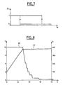
- the signal d i1 delivered by the current detecting element 14 1 is a hysteresis illustrated in FIG. 7, where the output d i1 is seen as a function of the shunt intensity i d .
- the charging is carried out in several phases illustrated in FIG. 8, where the curve 81 represents the voltage at the terminals of the module 20 as a function of the time t, and the curve 82 represents the charging intensity of the module 20 as a function of time. t also.
- I Cmax being the maximum charging current
- I Cmin the minimum charging current, less than I dN and di / dt the slope of the charging current.
- the charging current is linearly decreased in the limit of its minimum value, with a zero slope if d i is in the activated state and not zero otherwise.
- the third embodiment (function of detection of current associated with the voltage detection function) in relationship with the use of the second (voltage detection function only), but it is obvious that the current detection function can be used alone in combination with the branch circuit according to the invention and without the voltage detection function.
- the invention in all its embodiments, applies both the control of the load of a supercapacitor the balancing of a module of several supercapacities.
Landscapes
- Engineering & Computer Science (AREA)
- Power Engineering (AREA)
- Charge And Discharge Circuits For Batteries Or The Like (AREA)
Claims (15)
- Verfahren zum Ausgleichen von Superkapazitäten, bestehend aus der Abzweigung der in der Superkapazität fließenden Stromstärke ab einer vorbestimmten Klemmenspannung der Superkapazität, genannt Schwellenspannung, wobei die Abzweigungsstromstärke von der Klemmenspannung der Superkapazität abhängig ist, welche entsprechend dieser Spannung kontinuierlich ansteigt,
darin gekennzeichnet, dass die Abzweigungsstromstärke zwischen der Schwellenspannung, für welche die Abzweigungsstromstärke minimale Abzweigungsstromstärke genannt wird, und einer sogenannten Referenzspannung, für welche die Abzweigungsstromstärke nominale Abzweigungsstromstärke genannt wird, ansteigt, und dass der Unterschied zwischen der Referenzspannung und der Schwellenspannung kleiner als 200 mV ist und das Verhältnis zwischen der nominalen und der minimalen Abzweigungsstromstärke größer als 100 ist. - Verfahren nach Anspruch 1, in welchem die Abzweigungsstromstärke linear entsprechend der Klemmenspannung der Superkapazität ansteigt.
- Verfahren nach einem der Ansprüche 1 oder 2, in welchem die Abzweigungsstromstärke entsprechend der Klemmenspannung der Superkapazität begrenzt ist.
- Verfahren nach einem der Ansprüche 1 bis 3, in welchem die Referenzspannung der Spannung des Ladeendes der Superkapazität entspricht.
- Verfahren nach einem der Ansprüche 1 bis 3, in welchem die Schwellenspannung der Spannung des Ladeendes der Superkapazität entspricht.
- Verfahren nach einem der Ansprüche 1 bis 5, ferner bestehend aus der Steuerung der Ladeintensität der Superkapazität entsprechend deren Klemmenspannung durch eine logische Funktion der Spannungserkennung, die in der Lage ist, von einem aktivierten in einen deaktivierten Zustand überzugehen, wenn die Klemmenspannung der Superkapazität die Referenzspannung übersteigt, so dass die Ladeintensität der Superkapazität somit verringert ist, dann in den aktivierten Zustand zurückkehrt, wenn die Klemmenspannung der Superkapazität kleiner wird als eine minimale Steuerspannung.
- Verfahren nach Anspruch 6, in welchem das von der Funktion der Spannungserkennung ausgegebene Signal ein Signal in Form einer Hysterese ist.
- Verfahren nach einem der Ansprüche 1 bis 7, ferner bestehend aus der Steuerung der Ladeintensität der Superkapazität entsprechend der Abzweigungsstromstärke durch eine logische Funktion der Stromerkennung, die in der Lage ist, von einem aktivierten in einen deaktivierten Zustand überzugehen, wenn die Abzweigungsstromstärke die nominale Abzweigungsstromstärke übersteigt, so dass die Ladeintensität der Superkapazität somit verringert ist, dann in den aktivierten Zustand zurückkehrt, wenn die Abzweigungsstromstärke kleiner wird als eine minimale Steuerungsintensität.
- Verfahren nach Anspruch 8, in welchem das durch die Funktion der Stromerkennung ausgegebene Signal eine Hysterese ist.
- Vorrichtung zur Durchführung des Verfahrens nach einem der Ansprüche 1 bis 9, bestehend aus zumindest einer Superkapazität (11), an deren Klemmen ein Nebenkreis (12) parallelgeschaltet ist, der einen stromgesteuerten Leistungsverstärker, bestehend aus einem MOSFET-Transistor, einem bipolaren Transistor oder einem IGBT-Transistor, umfasst.
- Vorrichtung nach Anspruch 10, in welcher ein Erkennungsorgan (14), welches zumindest ein für die Klemmenspannung der Superkapazität (dv) und/oder die Abzweigungsstromstärke (d) repräsentatives Hysteresesignal ausgibt, mit dem Nebenkreis (12) verbunden ist und das Signal (dv, di) an Lademittel (15) der Superkapazität ausgibt.
- Vorrichtung nach Anspruch 10, bestehend aus mehreren in Serie geschalteten Superkapazitäten (111, ..., 115), einem Nebenkreis (121, ..., 125), der mit den Klemmen jeder Superkapazität (111, ..., 115) parallelgeschaltet ist.
- Verfahren nach den Ansprüchen 10 und 11, in welchem die durch die Gesamtheit der Erkennungsorgane (121, ..., 125) ausgegebenen Signale (dv1, ..., dv5, di1, ..., di5) durch eine logische UND-Funktion verbunden sind, deren Ausgabe an die Lademittel (15)gesendet wird.
- Vorrichtung nach Anspruch 10, bestehend aus mehreren in Serie geschalteten Superkapazitäten, einem einzigen Nebenkreis, der mit den Klemmen aller Superkapazitäten parallelgeschaltet ist.
- Vorrichtung nach Anspruch 10, bestehend aus mehreren parallelgeschalteten Superkapazitäten, einem einzigen Nebenkreis, der mit den Klemmen aller Superkapazitäten parallelgeschaltet ist.
Applications Claiming Priority (2)
| Application Number | Priority Date | Filing Date | Title |
|---|---|---|---|
| FR0107959 | 2001-06-18 | ||
| FR0107959A FR2826202B1 (fr) | 2001-06-18 | 2001-06-18 | Procede et dispositif d'equilibrage de supercapacite |
Publications (2)
| Publication Number | Publication Date |
|---|---|
| EP1274106A1 EP1274106A1 (de) | 2003-01-08 |
| EP1274106B1 true EP1274106B1 (de) | 2005-11-02 |
Family
ID=8864437
Family Applications (1)
| Application Number | Title | Priority Date | Filing Date |
|---|---|---|---|
| EP02291431A Expired - Lifetime EP1274106B1 (de) | 2001-06-18 | 2002-06-10 | Ausgleichsverfahren und -vorrichtung für einen Superkondensator |
Country Status (4)
| Country | Link |
|---|---|
| US (1) | US6664766B2 (de) |
| EP (1) | EP1274106B1 (de) |
| DE (1) | DE60207010T2 (de) |
| FR (1) | FR2826202B1 (de) |
Families Citing this family (23)
| Publication number | Priority date | Publication date | Assignee | Title |
|---|---|---|---|---|
| AU2002951291A0 (en) * | 2002-09-09 | 2002-09-19 | Energy Storage Systems Pty Ltd | A power supply |
| US20060264188A1 (en) * | 2003-08-29 | 2006-11-23 | Pierre Mars | Power supply for a communications module that demands high power during predetermined periods |
| CN100576687C (zh) * | 2003-12-17 | 2009-12-30 | 皇家飞利浦电子股份有限公司 | 应急照明设备 |
| US7541782B2 (en) * | 2004-03-30 | 2009-06-02 | Intel Corporation | System and method for extracting energy from an ultracapacitor |
| US7245185B2 (en) * | 2004-06-18 | 2007-07-17 | Bose Corporation | Controlling a power converter |
| US7880330B2 (en) * | 2004-06-18 | 2011-02-01 | Bose Corporation | Controlling a power converter |
| US7109686B2 (en) * | 2004-11-15 | 2006-09-19 | Ise Corporation | System and method for precharging and discharging a high power ultracapacitor pack |
| DE202005010858U1 (de) * | 2005-05-21 | 2006-09-28 | Diehl Luftfahrt Elektronik Gmbh | Vorrichtung zum Überwachen und Steuern mehrerer in Serie geschalteter Kapazitäten |
| FI118287B (fi) * | 2005-06-06 | 2007-09-14 | Abb Oy | Menetelmä ja järjestely taajuusmuuttajan tasajännitevälipiirin kondensaattoreiden lataamiseksi |
| DE102005034588A1 (de) * | 2005-07-25 | 2007-02-01 | Temic Automotive Electric Motors Gmbh | Energiespeicher |
| US20070112485A1 (en) * | 2005-11-17 | 2007-05-17 | Snap-On Incorporated | Vehicle service device and system powered by capacitive power source |
| US7696729B2 (en) * | 2006-05-02 | 2010-04-13 | Advanced Desalination Inc. | Configurable power tank |
| US20080129253A1 (en) * | 2006-11-03 | 2008-06-05 | Advanced Desalination Inc. | Battery energy reclamation apparatus and method thereby |
| US7471068B2 (en) * | 2006-11-03 | 2008-12-30 | Ivus Industries, Llc | Ultra-fast ultracapacitor charging method and charger |
| US7656061B2 (en) * | 2007-10-29 | 2010-02-02 | Bose Corporation | Automatic power source configuration |
| US7888907B2 (en) * | 2007-10-30 | 2011-02-15 | Bose Corporation | Controlled charging and use of power source |
| US8203281B2 (en) * | 2008-04-29 | 2012-06-19 | Ivus Industries, Llc | Wide voltage, high efficiency LED driver circuit |
| TWI377758B (en) * | 2008-06-20 | 2012-11-21 | Green Solution Tech Co Ltd | The battery charging controller and battery module thereof |
| KR101273811B1 (ko) * | 2010-10-25 | 2013-06-11 | 삼성전기주식회사 | 에너지 저장체의 전압 안정화 장치 및 그 방법 |
| US20120119709A1 (en) * | 2010-11-17 | 2012-05-17 | Tenergy Corporation | Battery pack balancing circuit |
| FR3033028B1 (fr) * | 2015-02-25 | 2019-12-27 | Safran Helicopter Engines | Chambre de combustion de turbomachine comportant une piece penetrante avec ouverture |
| US10374440B2 (en) | 2017-06-22 | 2019-08-06 | Rockwell Collins, Inc. | System and method for supercapacitor charging and balancing |
| DE102021200924B4 (de) * | 2021-02-02 | 2025-05-28 | SWJ Germany GmbH | Schaltungsanordnung mit zumindest einem Superkondensator und wenigstens einer Bypass-Schaltung, elektrischer Energiespeicher mit einer Schaltungsanordnung und Verwendung einer Schaltungsanordnung als Energiespeicher |
Family Cites Families (9)
| Publication number | Priority date | Publication date | Assignee | Title |
|---|---|---|---|---|
| US3732490A (en) * | 1971-06-07 | 1973-05-08 | Hewlett Packard Co | Impedance probe for swept network analyzer system |
| US5444378A (en) * | 1988-07-13 | 1995-08-22 | Electronic Development Inc. | Battery state of charge monitor |
| US5063340A (en) * | 1990-10-25 | 1991-11-05 | Motorola, Inc. | Capacitive power supply having charge equalization circuit |
| JPH06343225A (ja) * | 1993-05-28 | 1994-12-13 | Asahi Glass Co Ltd | 蓄電電源装置 |
| US5545933A (en) * | 1993-09-28 | 1996-08-13 | Okamura Laboratory Inc. | Electric power storage apparatus |
| JP3174472B2 (ja) * | 1995-02-27 | 2001-06-11 | 株式会社岡村研究所 | 並列充電制御装置及び電力貯蔵装置並びに充電制御法 |
| JP3661725B2 (ja) * | 1996-12-20 | 2005-06-22 | 旭硝子株式会社 | 電源装置 |
| US6104759A (en) * | 1997-09-15 | 2000-08-15 | Research In Motion Limited | Power supply system for a packet-switched radio transmitter |
| CN1305199C (zh) * | 2000-09-29 | 2007-03-14 | 山洋电气株式会社 | 无停电电源装置、变换装置以及并联工作型变换装置 |
-
2001
- 2001-06-18 FR FR0107959A patent/FR2826202B1/fr not_active Expired - Fee Related
-
2002
- 2002-06-10 DE DE60207010T patent/DE60207010T2/de not_active Expired - Lifetime
- 2002-06-10 EP EP02291431A patent/EP1274106B1/de not_active Expired - Lifetime
- 2002-06-17 US US10/171,968 patent/US6664766B2/en not_active Expired - Fee Related
Also Published As
| Publication number | Publication date |
|---|---|
| US6664766B2 (en) | 2003-12-16 |
| US20030062876A1 (en) | 2003-04-03 |
| DE60207010T2 (de) | 2006-04-13 |
| FR2826202A1 (fr) | 2002-12-20 |
| FR2826202B1 (fr) | 2003-12-19 |
| DE60207010D1 (de) | 2005-12-08 |
| EP1274106A1 (de) | 2003-01-08 |
Similar Documents
| Publication | Publication Date | Title |
|---|---|---|
| EP1274106B1 (de) | Ausgleichsverfahren und -vorrichtung für einen Superkondensator | |
| EP1274105B1 (de) | Verfahren und Vorrichtung zum Ausbalancieren von Superkapazitäten | |
| EP0654887B1 (de) | Unterbrechungsfreie Stromversorgung mit gemeinsamem Nullleiter und Doppelaufwärtskonverter | |
| EP1854165B1 (de) | Verfahren zum ausgewogenen aufladen einer lithiumionen- oder lithium-polymer-batterie | |
| EP1685622B3 (de) | Gleichgewichts-ladeverfahren für eine lithiumionen- oder lithiumpolymerbatterie | |
| EP0691725B1 (de) | Regelungsvorrichtung für eine elektrische Akkumulatorbatterie | |
| FR2819653A1 (fr) | Commande d'un convertisseur de puissance pour une recherche automatique du point de puissance maximale | |
| EP0847124B1 (de) | Notstromversorgungseinrichtung zur provisorischen Stromversorgung im Falle eines Versagens der Hauptstromversorgung | |
| WO2015121564A1 (fr) | Systeme d'alimentation a tension continue configure pour precharger un condensateur de filtrage avant l'alimentation d'une charge | |
| EP0883051A1 (de) | System zur Bereitstellung einer geregelten Spannung | |
| FR2754955A1 (fr) | Dispositif de limitation de variations transitoires d'une tension d'alimentation | |
| FR2907911A1 (fr) | Controleur d'alternateur de vehicule. | |
| EP1383222B1 (de) | Batterielader | |
| EP1977514B1 (de) | Steuerung eines mos-transistors | |
| FR3108456A1 (fr) | Dispositif de décharge d’une capacité | |
| CA3183945A1 (fr) | Procede de pilotage de charge et de decharge d'une pluralite de dispositifs de stockage d'energie electrique | |
| WO2018091491A1 (fr) | Système d'équilibrage local analogique pour un ensemble de dispositifs de stockage d'énergie électrique par effet capacitif, module de stockage rechargeable, véhicule de transport et installation électriques comprenant un tel système | |
| EP0453040A1 (de) | Leistungsverstärker, insbesondere für Rechtecksignale | |
| WO2020011768A1 (fr) | Procede de declenchement de la mise a l'etat passant d'un transistor | |
| FR3111490A1 (fr) | Convertisseur de tension dc/dc avec dispositif de precharge | |
| FR3045216B1 (fr) | Batterie comprenant une pluralite de cellules en serie | |
| FR3093247A1 (fr) | Système d’équilibrage, en tension basse, pour un ensemble de dispositifs de stockage d’énergie par effet capacitif (DESEEC). | |
| EP4639705A1 (de) | Solaranlage mit fotovoltaischen paneelen | |
| EP3453558B1 (de) | Einspeisungsmodul elektrischer leistung eines motorblocks, entsprechendes einspeisungsverfahren, zugsystem und fahrzeug | |
| FR2780599A1 (fr) | Circuit electrique d'eclairage d'un dispositif indicateur de vehicule automobile comportant des moyens de commande et d'asservissement |
Legal Events
| Date | Code | Title | Description |
|---|---|---|---|
| PUAI | Public reference made under article 153(3) epc to a published international application that has entered the european phase |
Free format text: ORIGINAL CODE: 0009012 |
|
| AK | Designated contracting states |
Kind code of ref document: A1 Designated state(s): AT BE CH CY DE DK ES FI FR GB GR IE IT LI LU MC NL PT SE TR |
|
| AX | Request for extension of the european patent |
Free format text: AL;LT;LV;MK;RO;SI |
|
| 17P | Request for examination filed |
Effective date: 20030708 |
|
| AKX | Designation fees paid |
Designated state(s): DE FR GB |
|
| GRAP | Despatch of communication of intention to grant a patent |
Free format text: ORIGINAL CODE: EPIDOSNIGR1 |
|
| RAP1 | Party data changed (applicant data changed or rights of an application transferred) |
Owner name: SAFT FINANCE S.AE.R.L. |
|
| RIN1 | Information on inventor provided before grant (corrected) |
Inventor name: BARRAILH, GERARD Inventor name: ROCHARD, DAMIEN Inventor name: DESPREZ, PHILIPPE Inventor name: SHARIF, FADI Inventor name: DAVAT, BERNARD Inventor name: RAEL, STEPHANE |
|
| GRAS | Grant fee paid |
Free format text: ORIGINAL CODE: EPIDOSNIGR3 |
|
| GRAA | (expected) grant |
Free format text: ORIGINAL CODE: 0009210 |
|
| AK | Designated contracting states |
Kind code of ref document: B1 Designated state(s): DE FR GB |
|
| REG | Reference to a national code |
Ref country code: GB Ref legal event code: FG4D Free format text: NOT ENGLISH |
|
| REF | Corresponds to: |
Ref document number: 60207010 Country of ref document: DE Date of ref document: 20051208 Kind code of ref document: P |
|
| GBT | Gb: translation of ep patent filed (gb section 77(6)(a)/1977) |
Effective date: 20051125 |
|
| PLBE | No opposition filed within time limit |
Free format text: ORIGINAL CODE: 0009261 |
|
| STAA | Information on the status of an ep patent application or granted ep patent |
Free format text: STATUS: NO OPPOSITION FILED WITHIN TIME LIMIT |
|
| 26N | No opposition filed |
Effective date: 20060803 |
|
| PGFP | Annual fee paid to national office [announced via postgrant information from national office to epo] |
Ref country code: DE Payment date: 20130621 Year of fee payment: 12 Ref country code: GB Payment date: 20130606 Year of fee payment: 12 |
|
| REG | Reference to a national code |
Ref country code: DE Ref legal event code: R119 Ref document number: 60207010 Country of ref document: DE |
|
| GBPC | Gb: european patent ceased through non-payment of renewal fee |
Effective date: 20140610 |
|
| REG | Reference to a national code |
Ref country code: DE Ref legal event code: R119 Ref document number: 60207010 Country of ref document: DE Effective date: 20150101 |
|
| PG25 | Lapsed in a contracting state [announced via postgrant information from national office to epo] |
Ref country code: DE Free format text: LAPSE BECAUSE OF NON-PAYMENT OF DUE FEES Effective date: 20150101 |
|
| PG25 | Lapsed in a contracting state [announced via postgrant information from national office to epo] |
Ref country code: GB Free format text: LAPSE BECAUSE OF NON-PAYMENT OF DUE FEES Effective date: 20140610 |
|
| REG | Reference to a national code |
Ref country code: FR Ref legal event code: PLFP Year of fee payment: 15 |
|
| PGFP | Annual fee paid to national office [announced via postgrant information from national office to epo] |
Ref country code: FR Payment date: 20160603 Year of fee payment: 15 |
|
| REG | Reference to a national code |
Ref country code: FR Ref legal event code: ST Effective date: 20180228 |
|
| PG25 | Lapsed in a contracting state [announced via postgrant information from national office to epo] |
Ref country code: FR Free format text: LAPSE BECAUSE OF NON-PAYMENT OF DUE FEES Effective date: 20170630 |