EP1274129A2 - Dispositif électronique et méthode associée - Google Patents
Dispositif électronique et méthode associée Download PDFInfo
- Publication number
- EP1274129A2 EP1274129A2 EP02012596A EP02012596A EP1274129A2 EP 1274129 A2 EP1274129 A2 EP 1274129A2 EP 02012596 A EP02012596 A EP 02012596A EP 02012596 A EP02012596 A EP 02012596A EP 1274129 A2 EP1274129 A2 EP 1274129A2
- Authority
- EP
- European Patent Office
- Prior art keywords
- heat sink
- component
- connection
- components
- diodes
- Prior art date
- Legal status (The legal status is an assumption and is not a legal conclusion. Google has not performed a legal analysis and makes no representation as to the accuracy of the status listed.)
- Ceased
Links
Images

Classifications
-
- H—ELECTRICITY
- H10—SEMICONDUCTOR DEVICES; ELECTRIC SOLID-STATE DEVICES NOT OTHERWISE PROVIDED FOR
- H10W—GENERIC PACKAGES, INTERCONNECTIONS, CONNECTORS OR OTHER CONSTRUCTIONAL DETAILS OF DEVICES COVERED BY CLASS H10
- H10W90/00—Package configurations
Definitions
- Bridge rectifier circuits are known in which two commutation groups are formed in that For example, three power semiconductor components on one Heat sinks can be combined so that two Commutation groups form the bridge circuit arrangement and the heat sinks of the respective commutation groups are electrically isolated from each other.
- the electrical arrangement according to the invention and the method has the advantage that Power semiconductor components on a heat sink are provided, which are connected to the heat sink Parts of the power semiconductor components different can have electrical polarity, so that the Heatsink parts to be insulated electrically from each other Power semiconductor devices cool and that it at the same time it is possible that Power semiconductor components on a heat sink are housed, although they have different polarity exhibit.
- commutation groups do not have to for example, housed two different heat sinks are provided that are electrically insulated from each other and where the insulating layers between the as Commutation groups provided the heat sinks Limit heat dissipation from the semiconductor components and so because of the limited permissible maximum temperature of the pn junction (junction temperature) a greater performance of the Semiconductor components required.
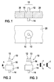
- Figure 1 is a semiconductor device 10, which in The following is simply called component 10, shown, which is connected to a heat sink 20.
- the component 10 is in particular as Power semiconductor device provided, i.e. the Component 10 comprises a power semiconductor.
- the Component 10 comprises a first connection 12 and one second connector 14, the second connector 14 being electrical is connected to a base 15 via which the component 10 is connected to the heat sink 20.
- the base 15 has Essentially a cylindrical or conical one Lateral surface, which with a bore (without reference number) cooperates in the heat sink 20, so that a mechanical Connection between the heat sink 20 and the component 10 can be produced.
- In the upper part of Figure 1 is one Side view of the arrangement of component 10 and heat sink 20 shown, while in the lower part of Figure 1 a Top view of heat sink 20 and component 10 is shown is.
- the component 10 is a based on the example bipolar component 10 shown, in the example one Diode, which in the left part of Figure 2 as a switching symbol with a connection provided with the reference symbol A, the represents the anode, and with one with the reference symbol K provided connector, which represents the cathode, is provided.
- the base 15 of the Component 10, which in turn connects to the in FIG. 2 ensures heat sink 20, not shown, furthermore a housing 16 of the component 10, which in Essentially above the base 15 with an im A substantially smaller diameter is provided. Above of the housing 16 protrudes the first. Connection 12 from the Component 10 or from the housing 16 of the component 10 out.
- the first connection 12 is in particular one Diode provided as head wire.
- the base from which in leads out lower part of the second connection 14 is with the second terminal 14 electrically connected.
- the component is a based on the example three-pole component 10 according to the invention, 3 examples of Circuit symbols of such three-pole components, in particular.
- Transistors are shown.
- it is a MOS power transistor, which one with the Reference symbol S (source) designated connection, one with the reference symbol D (drain) and a connection connection designated by the reference symbol G (gate) having.
- the symbolic representation shown a bipolar transistor, which one with the Reference symbol E (emitter) shown connection, one with the reference symbol C (collector) and a connection provided with the reference symbol B (base) having.
- Component 10 shown in a manner analogous to FIG. 2, the same reference numerals the same parts of the component 10 correspond, but in contrast to Figure 2 from the housing 16 not a single first connection 12 but a third connection 13 is led out, so that the three connections of the three-pole component are taken into account are.
- FIG. 4 is a rectifier circuit as an example represented an electrical arrangement according to the invention.
- the rectifier arrangement according to FIG. 4 comprises a total six power semiconductor diodes as examples of Components 10.
- Three first diodes, which with the Reference numerals 30 are provided with their anode on three, provided with the reference symbols R, S and T. Connected input connections and with their cathode with an exit marked with a plus sign electrical arrangement connected.
- Three more second Diodes which are provided with the reference symbol 31 are marked with the inputs R, S, T via their cathode connection connected and together with their anode connection form the output connection line with a minus sign electrical arrangement.
- On those with a plus or minus sign provided output lines of the electrical arrangement a pulsating but rectified tension tapped if one at the inputs R, S, T AC voltage is present.
- FIG. 5 The physical realization of a rectifier circuit 4 is shown in FIG. 5.
- Figure 5 In the upper part Figure 5 is a bottom view of the electrical Arrangement shown, in the middle is a Side view of the electrical arrangement shown and in lower part of FIG. 5 is a top view of FIG electrical arrangement shown.
- the top view is the heat sink 20 is shown, with which the first diodes 30 and the second diodes 31 are connected.
- second connections 14 of the diodes 30, 31 the serve as an example for general components 10 are a first input rail 141, a second input rail 142 and a third input rail 143 connected via which the three circuit inputs, which in Figure 4 with the Reference numerals R, S, T are designated, are realized.
- first Diodes 30, the second diodes 31 and the input rails 141, 142, 143 are again the heat sink 20, the first Diodes 30, the second diodes 31 and the input rails 141, 142, 143.
- Side view of a first current output rail 121 and one shown second current output rail 122 which the Outputs of those shown in Figure 4 Rectifier circuit correspond.
- One of the two Current output rails 121, 122 correspond to the positive Output line (provided with a plus sign in FIG. 4) and the other of the two power output rails 121, 122 corresponds to the negative output (with a minus sign provided) of Figure 4.
- the heat sink 20 is of the diodes 30, 31 or general of any component 10 according to the invention, provided in isolation. This is according to the invention achieved an insulating layer between the heat sink 20 and the component 10 is provided.
- the insulation layer is for example in the form of an anodized layer on the Heatsink 20, which in this case, for example Aluminum is made, or in the form of a paint job Heat sink 20 with, for example, conventional wire enamel intended.
- it is provided according to the invention instead of or in addition to anodizing and / or the Painting a coating of the heat sink 20 by means of a ceramic and / or a powder coating provided.
- the heat sink 20 has six holes for receiving of diodes 30, 31 and generally for the inclusion of Components 10 according to the invention provided.
- the above The anodized layer mentioned is used, for example, with a Heat sink 20 made of aluminum according to the mechanical Processing, i.e. the creation of the holes.
- the heat sink material and the tolerance of the holes are the material and the diameter of the base 15 of the Adjust components 10 so that a sufficient pressure the base 15 of the components 10 in the intended Temperature range is guaranteed.
- an anodized layer offers sufficient Puncture resistance between the heat sink 20 and the Socket 15 of the components 10.
- the dielectric strength is caused by a voltage additional painting of the heat sink 20 with conventional Wire enamel increased.
- the bases of the components 10 are not in the heat sink 20 pressed in, but shrunk without force.
- Such a connection between the components 10 and the heat sink 20 is also after shrinking the Components 10 are still reliable, i.e. the components 10 cannot "fall out" of the heat sink 20 because the Components 10 in later operation as a result of their Self-heating are always hotter than the heat sink 20, i.e. have a higher temperature than the heat sink 20.
- passivation of the heat sink passivation of the component 10 - in particular its Base 15 - is for example by means of the above specified processes such as anodizing and / or painting and / or coating provided.
- a diode as shown in FIG. 2 provided component 10 can be provided both in this way can that the cathode at the first terminal 12 and the anode is provided at the second connection 14, as well as such be provided that the anode at the first terminal 12 and the cathode is provided on the second connection 14.
- the diodes 30, 31 in the arrangement shown in Figure 5 according to the invention are generally introduced into the heat sink 20 in such a way that the housing 16 or the first connection 12 on the same side of the heat sink 20 is provided. Since on the same side of the heat sink 20 both the first and the second power output rail is provided, the first diodes 30 may be connected in reverse to that second diodes 31, i.e. the first and second ports 12, 14 with the first diodes 30 and the second diodes 31 be reversed.
- connection of the first and second connections 12, 14 of the Components 10, but also the third connection 13 of the Components 10 with the current output rails 121, 122 or the current input rails 141, 142, 143 takes place with the known techniques, i.e. Soldering, welding, crimping (radial crimping of a sleeve on a pin) or like.
- a component is also provided connect a heat sink, the component electrical connections only on one side of the component 10 having.
Landscapes
- Rectifiers (AREA)
- Cooling Or The Like Of Semiconductors Or Solid State Devices (AREA)
Applications Claiming Priority (2)
| Application Number | Priority Date | Filing Date | Title |
|---|---|---|---|
| DE10132455 | 2001-07-04 | ||
| DE10132455A DE10132455B4 (de) | 2001-07-04 | 2001-07-04 | Elektrische Anordnung mit einem Kühlkörper und Verfahren zu deren Herstellung |
Publications (2)
| Publication Number | Publication Date |
|---|---|
| EP1274129A2 true EP1274129A2 (fr) | 2003-01-08 |
| EP1274129A3 EP1274129A3 (fr) | 2004-12-01 |
Family
ID=7690610
Family Applications (1)
| Application Number | Title | Priority Date | Filing Date |
|---|---|---|---|
| EP02012596A Ceased EP1274129A3 (fr) | 2001-07-04 | 2002-06-06 | Dispositif électronique et méthode associée |
Country Status (2)
| Country | Link |
|---|---|
| EP (1) | EP1274129A3 (fr) |
| DE (1) | DE10132455B4 (fr) |
Cited By (1)
| Publication number | Priority date | Publication date | Assignee | Title |
|---|---|---|---|---|
| EP1460749A1 (fr) * | 2003-03-17 | 2004-09-22 | Hitachi, Ltd. | Machine électrique multiphase à courant alternatif |
Families Citing this family (2)
| Publication number | Priority date | Publication date | Assignee | Title |
|---|---|---|---|---|
| DE102006019315B4 (de) * | 2006-04-26 | 2015-04-16 | Robert Bosch Gmbh | Gleichrichter für eine Elektromaschine |
| DE102012207470B3 (de) * | 2012-05-04 | 2013-10-10 | Infineon Technologies Ag | Verfahren zur herstellung einer halbleitermodulanordnung |
Family Cites Families (5)
| Publication number | Priority date | Publication date | Assignee | Title |
|---|---|---|---|---|
| DE1489170A1 (de) * | 1963-08-08 | 1969-05-22 | Ngk Insulators Ltd | Halbleitervorrichtung |
| DE2649418A1 (de) * | 1976-10-29 | 1978-05-03 | Bosch Gmbh Robert | Gleichrichtereinheit |
| DE2826898A1 (de) * | 1978-06-19 | 1980-01-03 | Siemens Ag | Kuehlkoerper fuer elektrische bauelemente |
| US5461766A (en) * | 1994-01-26 | 1995-10-31 | Sun Microsystems, Inc. | Method for integrally packaging an integrated circuit with a heat transfer apparatus |
| DE4403996A1 (de) * | 1994-02-09 | 1995-08-10 | Bosch Gmbh Robert | Gleichrichteranordnung für einen Drehstromgenerator |
-
2001
- 2001-07-04 DE DE10132455A patent/DE10132455B4/de not_active Expired - Fee Related
-
2002
- 2002-06-06 EP EP02012596A patent/EP1274129A3/fr not_active Ceased
Cited By (2)
| Publication number | Priority date | Publication date | Assignee | Title |
|---|---|---|---|---|
| EP1460749A1 (fr) * | 2003-03-17 | 2004-09-22 | Hitachi, Ltd. | Machine électrique multiphase à courant alternatif |
| US7075201B2 (en) | 2003-03-17 | 2006-07-11 | Hitachi, Ltd. | Multi-phase alternating-current rotational electric machine |
Also Published As
| Publication number | Publication date |
|---|---|
| DE10132455A1 (de) | 2003-01-30 |
| DE10132455B4 (de) | 2009-12-17 |
| EP1274129A3 (fr) | 2004-12-01 |
Similar Documents
| Publication | Publication Date | Title |
|---|---|---|
| DE102007013186B4 (de) | Halbleitermodul mit Halbleiterchips und Verfahren zur Herstellung desselben | |
| DE112015000245T5 (de) | Halbleitermodul | |
| DE102017213288B4 (de) | Halbleitermodul, Halbleitervorrichtung und elektrische Leistungsvorrichtung | |
| DE102007012154A1 (de) | Halbleitermodul mit Halbleiterchips und Verfahren zur Herstellung desselben | |
| DE102017120747B4 (de) | SMD-Gehäuse mit Oberseitenkühlung und Verfahren zu seiner Bereitstellung | |
| DE102008001414A1 (de) | Substrat-Schaltungsmodul mit Bauteilen in mehreren Kontaktierungsebenen | |
| DE102006012781A1 (de) | Multichip-Modul mit verbessertem Systemträger | |
| DE3544324C2 (de) | Integrierte MOS-Leistungsbrückenschaltung sowie Verfahren zu deren Herstellung | |
| DE112012006842B4 (de) | Halbleitervorrichtung | |
| DE102018104972A1 (de) | Leiterplattenelement mit integriertem elektronischen Schaltelement, Stromrichter und Verfahren zum Herstellen eines Leiterplattenelements | |
| DE102017101185B4 (de) | Ein Halbleitermodul umfassend Transistorchips, Diodenchips und Treiberchips, angeordnet in einer gemeinsamen Ebene, Verfahren zu dessen Herstellung und integriertes Leistungsmodul | |
| DE102017212739A1 (de) | Halbleiterbauteil sowie Verfahren zu dessen Herstellung | |
| DE102015104995B4 (de) | Verbindungshalbleitervorrichtung mit einem mehrstufigen Träger | |
| DE102004059313B3 (de) | Leistungshalbleitermodul mit verringerten parasitären Induktivitäten | |
| DE102017108172B4 (de) | SMD-Package und Verfahren zur Herstellung eines SMD-Packages | |
| DE102013113143B4 (de) | Leistungshalbleitereinrichtung | |
| DE10340297A1 (de) | Schaltungsanordnung für aktive und passive elektrische und elektronische Bauelemente | |
| DE102017207564A1 (de) | Halbleitermodul | |
| DE10132455B4 (de) | Elektrische Anordnung mit einem Kühlkörper und Verfahren zu deren Herstellung | |
| DE102018002731A1 (de) | Motorantriebsvorrichtung | |
| DE102012201889A1 (de) | Elektrisches Leistungsmodul und Verfahren und Vorrichtung zum Herstellen eines elektrischen Leistungsmoduls | |
| DE112022006834T5 (de) | Leistungsmodulhalbleitergehäuse und Halbleitervorrichtung | |
| DE102015115140B4 (de) | Stromrichteranordnung mit verbesserter Befestigung | |
| DE102007016901B4 (de) | Halbleiterbauelement und elektronisches Modul | |
| DE102015103667A1 (de) | Leistungshalbleitermodul mit verbesserter Bondverbindungstruktur |
Legal Events
| Date | Code | Title | Description |
|---|---|---|---|
| PUAI | Public reference made under article 153(3) epc to a published international application that has entered the european phase |
Free format text: ORIGINAL CODE: 0009012 |
|
| AK | Designated contracting states |
Kind code of ref document: A2 Designated state(s): AT BE CH CY DE DK ES FI FR GB GR IE IT LI LU MC NL PT SE TR |
|
| AX | Request for extension of the european patent |
Free format text: AL;LT;LV;MK;RO;SI |
|
| PUAL | Search report despatched |
Free format text: ORIGINAL CODE: 0009013 |
|
| AK | Designated contracting states |
Kind code of ref document: A3 Designated state(s): AT BE CH CY DE DK ES FI FR GB GR IE IT LI LU MC NL PT SE TR |
|
| AX | Request for extension of the european patent |
Extension state: AL LT LV MK RO SI |
|
| 17P | Request for examination filed |
Effective date: 20050601 |
|
| AKX | Designation fees paid |
Designated state(s): DE ES FR GB IT SE |
|
| 18R | Application refused |
Effective date: 20080405 |
|
| STAA | Information on the status of an ep patent application or granted ep patent |
Free format text: STATUS: THE APPLICATION HAS BEEN REFUSED |
|
| R18R | Application refused (corrected) |
Effective date: 20080404 |