EP1274230A2 - Austastpegel-Steuerungsschaltung und Verfahren zur Steuerung des Austastpegels - Google Patents
Austastpegel-Steuerungsschaltung und Verfahren zur Steuerung des Austastpegels Download PDFInfo
- Publication number
- EP1274230A2 EP1274230A2 EP02013981A EP02013981A EP1274230A2 EP 1274230 A2 EP1274230 A2 EP 1274230A2 EP 02013981 A EP02013981 A EP 02013981A EP 02013981 A EP02013981 A EP 02013981A EP 1274230 A2 EP1274230 A2 EP 1274230A2
- Authority
- EP
- European Patent Office
- Prior art keywords
- pedestal level
- signal
- video
- video signal
- data signal
- Prior art date
- Legal status (The legal status is an assumption and is not a legal conclusion. Google has not performed a legal analysis and makes no representation as to the accuracy of the status listed.)
- Withdrawn
Links
Images


Classifications
-
- H—ELECTRICITY
- H04—ELECTRIC COMMUNICATION TECHNIQUE
- H04N—PICTORIAL COMMUNICATION, e.g. TELEVISION
- H04N5/00—Details of television systems
- H04N5/44—Receiver circuitry for the reception of television signals according to analogue transmission standards
- H04N5/57—Control of contrast or brightness
-
- H—ELECTRICITY
- H04—ELECTRIC COMMUNICATION TECHNIQUE
- H04N—PICTORIAL COMMUNICATION, e.g. TELEVISION
- H04N21/00—Selective content distribution, e.g. interactive television or video on demand [VOD]
- H04N21/40—Client devices specifically adapted for the reception of or interaction with content, e.g. set-top-box [STB]; Operations thereof
- H04N21/41—Structure of client; Structure of client peripherals
- H04N21/426—Internal components of the client ; Characteristics thereof
-
- H—ELECTRICITY
- H04—ELECTRIC COMMUNICATION TECHNIQUE
- H04N—PICTORIAL COMMUNICATION, e.g. TELEVISION
- H04N5/00—Details of television systems
- H04N5/14—Picture signal circuitry for video frequency region
- H04N5/16—Circuitry for reinsertion of DC and slowly varying components of signal; Circuitry for preservation of black or white level
-
- H—ELECTRICITY
- H04—ELECTRIC COMMUNICATION TECHNIQUE
- H04N—PICTORIAL COMMUNICATION, e.g. TELEVISION
- H04N9/00—Details of colour television systems
- H04N9/64—Circuits for processing colour signals
- H04N9/73—Colour balance circuits, e.g. white balance circuits or colour temperature control
-
- H—ELECTRICITY
- H04—ELECTRIC COMMUNICATION TECHNIQUE
- H04N—PICTORIAL COMMUNICATION, e.g. TELEVISION
- H04N21/00—Selective content distribution, e.g. interactive television or video on demand [VOD]
- H04N21/40—Client devices specifically adapted for the reception of or interaction with content, e.g. set-top-box [STB]; Operations thereof
- H04N21/43—Processing of content or additional data, e.g. demultiplexing additional data from a digital video stream; Elementary client operations, e.g. monitoring of home network or synchronising decoder's clock; Client middleware
- H04N21/431—Generation of visual interfaces for content selection or interaction; Content or additional data rendering
- H04N21/4318—Generation of visual interfaces for content selection or interaction; Content or additional data rendering by altering the content in the rendering process, e.g. blanking, blurring or masking an image region
-
- H—ELECTRICITY
- H04—ELECTRIC COMMUNICATION TECHNIQUE
- H04N—PICTORIAL COMMUNICATION, e.g. TELEVISION
- H04N5/00—Details of television systems
- H04N5/44—Receiver circuitry for the reception of television signals according to analogue transmission standards
Definitions
- the present invention relates to a technology in pedestal level control circuits for video signal processing in a television receiver, etc., more precisely, for pedestal level adjustment, such as brightness adjustment, cutoff adjustment for adjusting white balance of color video images.
- the pedestal level of a video signal output from a tuner or the like is not always constant. Therefore, for brightness adjustment, the pedestal level is clamped to a predetermined level and then is offset by a predetermined amount.
- cutoff adjustment in which the pedestal level is adjusted in the above-described manner for video signals of each of, for example, R, G, and B (red, green, and blue) is performed in order to adjust white balance in accordance with non-uniformity in the emission of a cathode ray tube (CRT).
- CRT cathode ray tube
- a D/A converter 506 converts a digital adjustment data signal that is for brightness adjustment into an analog voltage signal.
- a brightness adjustment current output circuit 507 converts the analog voltage signal to a current signal and supplies it to the amplifier 505 so that the pedestal level of the video signal output from the amplifier 505 is set to a level in accordance with the brightness adjustment data.
- the clamp circuit 501 and the clamp circuit 502 both use the same reference voltage source 503 , so that the pedestal levels of the internal and external video signals are clamped to the same level to eliminate fluctuations in the pedestal level.
- the brightness adjustment is performed by offsetting the pedestal level in accordance with the brightness adjustment data, based on the pedestal levels of the same level, so that there is no difference in the basic luminance of video images to be displayed, regardless of which the switch 504 is directed to.
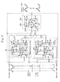
- Figure 10 shows another conventional pedestal level control circuit (brightness and cutoff adjustment circuit) which has a configuration for performing brightness adjustment and cutoff adjustment with respect to internal and external video signals of three channels of RGB.
- both the reference voltage source 503 and the D/A converter 506 are the same as those shown in Figure 9 .
- the clamp circuit 501 , the clamp circuit 502 , the switch 504 , and the amplifier 505 are provided for each of the R, G, and B video-signal channels.
- respective signal currents for cutoff adjustment are input to each amplifier 505 .
- the brightness adjustment current output circuit 507 outputs the signal current for brightness adjustment to the amplifiers 505 for R, G and B.
- a D/A converter 508 and a cutoff adjustment current output circuit 509 are provided.
- the D/A converter 508 converts a digital data signal for cutoff adjustment for each of R, G, and B to an analog voltage signal
- the cutoff adjustment current output circuit 509 converts the analog voltage signal to a current signal and supplies it to the amplifier 505 so that the pedestal level of the video signal output from each amplifier 505 is set to a level in accordance with the brightness adjustment data and the cutoff adjustment data.
- the pedestal levels for all the R, G, and B and the internal and external video signals are clamped to the same level. Therefore, regarding brightness adjustment, the pedestal levels are offset by an amount in accordance with the brightness adjustment data for all the cases.
- the pedestal level is offset by an amount in accordance with the cutoff adjustment data of each corresponding color. Therefore, there is no difference in the luminance of video images to be displayed, regardless of the switching of the switch 504 either to an internal video signal or an external video signal, and white balance suitable for non-uniformity in the emission of a CRT or the like can be obtained.
- the clamp circuit is provided for each video signal, so that the circuit scale tends to be large. Furthermore, it is necessary to perform brightness adjustment or cutoff adjustment after clamping the video signal. Therefore, for example, configuring elements or blocks subsequent to the clamp circuit in one IC chip requires input terminals (pins) to which the brightness adjustment signal or the like are input; digital input interfaces; power source circuits and power source terminals of two types for digital and analog signals; and lines between the IC chips (bus lines) or the like. Moreover, in a case in which the brightness adjustment or the like is performed based on digital signal processing and the D/A converter or the like is provided in the vicinity of the clamp circuit or the like, video signals are more susceptible to noise caused by the digital signals.
- a first pedestal level control circuit of the present invention includes a video data signal output means for outputting a digital video data signal; a pedestal level adjustment data signal output means for outputting a pedestal level adjustment data signal used to generate an analog video signal having a predetermined pedestal level; and a video signal generating means for generating the analog video signal having the predetermined pedestal level based on the video data signal and the pedestal level adjustment data signal.
- the video signal generating means includes a first D/A converting means for converting the video data signal output from the video data signal output means into an analog signal; a second D/A converting means for converting the pedestal level adjustment data signal output from the pedestal level adjustment data signal output means into an analog signal; and an analog signal synthesis means for generating the analog video signal having a predetermined pedestal level by synthesizing the analog signals converted by the first D/A converter and the second D/A converter.
- a plurality of sets are provided, each including the video data signal output means, the pedestal level adjustment data signal output means and the video signal generating means.
- a second pedestal level control circuit includes a holding means for holding a predetermined pedestal level of a first video signal; a clamping means for clamping a second video signal such that a pedestal level of the second video signal is equal to the pedestal level of the first video signal that is held; and a switching means for selectively switching the first video signal and the clamped second video signal to output the signal.
- the first video signal having a predetermined pedestal level is an analog video signal having a predetermined pedestal level that is generated based on a digital video data signal and a pedestal level adjustment data signal.
- each set including the holding means, the clamping means, and the switching means.
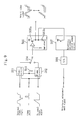
- Figure 1 is a block diagram showing a configuration of a brightness adjustment circuit of Embodiment 1.
- Figure 2 is a block diagram showing a configuration of a variation of the brightness adjustment circuit of Embodiment 1.
- Figure 3 is a block diagram showing a configuration of a brightness and cutoff adjustment circuit of Embodiment 2.
- Figure 9 is a block diagram showing a configuration of a conventional brightness adjustment circuit.
- Figure 10 is a block diagram showing a configuration of a conventional brightness and cutoff adjustment circuit.
- the D/A converters 103 and 104 perform D/A conversion of the video data signal and the brightness adjustment data signal, respectively, and output a video signal and a brightness adjustment signal, respectively, that are currents (analog signals) having a magnitude corresponding to these data signals.
- the analog signal synthesis circuit 105 synthesizes the video signal and the brightness adjustment signal by adding the currents, converts it to a voltage with a resistor 105a and outputs the video signal (voltage) that is brightness adjusted.
- the amplifier 106 amplifies the video signal.
- the D/A converter 103 outputs a video signal whose pedestal level is in a predetermined reference level, based on the video data signal output from the video data signal output section 101.
- the D/A converter 104 outputs a brightness adjustment signal of a level corresponding to an offset amount from the pedestal level of the predetermined reference.
- the video signal and the brightness adjustment signal are synthesized by the analog signal synthesis circuit 105 , so that a video signal that is brightness adjusted is output from the amplifier 106, and thus a display apparatus such as a CRT or a LCD (liquid crystal display) is driven.
- converters utilizing current outputs as above are used as the D/A converters 103 and 104, signals can be synthesized comparatively easily.
- the signal synthesis is not restricted by the dynamic range between the power source and GND, so that the dynamic range of output signals can be enlarged easily (therefore, it is possible to increase the resolution of D/A (graduation) without limit).
- the present invention is not limited to the converters utilizing current outputs, and also when converters utilizing voltage outputs are used, the advantages of the present invention as described above can be obtained.
- a brightness adjustment circuit for brightness adjusting a video signal in response to a video signal that has been brightness adjusted in the manner, for example, as described in Embodiment 1 will be described.
- an internal video signal generated inside a device in which a brightness adjustment circuit is provided and an external video signal that is externally input are selectively switched.
- Such switching is used, for example, to display a receiving channel number or character information by partial superimposition on broadcast video images, or to switch between broadcast video images and other video images by unit of one or more frame periods for display.
- the clamp circuit 123 is different from the sample/hold circuit 122 in the following points: An output from the second emitter follower circuit 145 of the sample/hold circuit 122 is input to the base of the transistor 151; the clamp switch 157 is configured so as to be on/off in response to a clamp pulse in synchronization with an external video signal; and an external video signal is input to one terminal of the capacitor 162.
- the pedestal level of the external video signal is clamped so as to be equal to the pedestal level of the internal video signal held in the sample/hold circuit 122.
- An amplifier 106 includes a differential amplifier 174, a voltage source 175, current sources 176 and 177, a third current mirror circuit 180, and a load resistor 181.
- the differential amplifier 174 includes transistors 171 and 172, and a resistor 173, and converts a voltage signal that is a video signal selected by the switch 121 to a current signal.
- the voltage source 175 generates a voltage that is used as the reference for the conversion from a voltage to a current.
- the current sources 176 and 177 supply current to the differential amplifier 174.
- the third current mirror circuit 180 includes transistors 178 and 179 and performs mirroring with respect to the collector currents of the two transistors.
- the load resistor 181 converts the collector current of the transistor 179 to a voltage. Thus, an amplified output video signal is output.
- the sampling pulse and the clamp pulse are the same signal, so that either one of them can be input to the sample/hold circuit 122 and the clamp circuit 123.
- sample/hold circuit 122 is not necessarily provided, and for example, as shown in broken lines in Figure 6, outputs from the D/A converter 104 or the analog signal synthesis circuit 105 or the like can be input directly to the clamp circuit 123 as the reference voltage. In this case, the circuit scale can be reduced further by omitting the sample/hold circuit 122.
- the pedestal levels of the internal video signals for R, G and B are equal to one another, as shown in Figure 8 , only one sample/hold circuit 122 may be provided to which one of the R, the G, and the B internal video signals is input, and the voltage held by that sample/hold circuit 122 may be input as the reference voltage to the clamp circuits 123.
- the pedestal level of other video signals can be adjusted with the typical video signal, so that the circuit scale can be suppressed to be small.
Landscapes
- Engineering & Computer Science (AREA)
- Multimedia (AREA)
- Signal Processing (AREA)
- Processing Of Color Television Signals (AREA)
- Picture Signal Circuits (AREA)
- Controls And Circuits For Display Device (AREA)
- Television Receiver Circuits (AREA)
Applications Claiming Priority (2)
| Application Number | Priority Date | Filing Date | Title |
|---|---|---|---|
| JP2001200539 | 2001-07-02 | ||
| JP2001200539A JP2003018429A (ja) | 2001-07-02 | 2001-07-02 | ペデスタルレベル制御回路、およびペデスタルレベル制御方法 |
Publications (2)
| Publication Number | Publication Date |
|---|---|
| EP1274230A2 true EP1274230A2 (de) | 2003-01-08 |
| EP1274230A3 EP1274230A3 (de) | 2005-03-30 |
Family
ID=19037648
Family Applications (1)
| Application Number | Title | Priority Date | Filing Date |
|---|---|---|---|
| EP02013981A Withdrawn EP1274230A3 (de) | 2001-07-02 | 2002-06-25 | Austastpegel-Steuerungsschaltung und Verfahren zur Steuerung des Austastpegels |
Country Status (4)
| Country | Link |
|---|---|
| US (1) | US7030936B2 (de) |
| EP (1) | EP1274230A3 (de) |
| JP (1) | JP2003018429A (de) |
| CN (2) | CN1395428A (de) |
Families Citing this family (8)
| Publication number | Priority date | Publication date | Assignee | Title |
|---|---|---|---|---|
| JP2004215184A (ja) * | 2003-01-08 | 2004-07-29 | Renesas Technology Corp | クランプ回路 |
| JP4487751B2 (ja) * | 2004-12-06 | 2010-06-23 | 船井電機株式会社 | テレビジョンおよびテレビジョンの調整方法 |
| US7327297B2 (en) * | 2006-06-30 | 2008-02-05 | Himax Technologies Limited | Source driver of liquid crystal display and the driving method |
| KR101741499B1 (ko) * | 2010-11-29 | 2017-05-31 | 삼성전자주식회사 | 페데스탈 레벨 보상 방법 및 이를 수행할 수 있는 장치들 |
| KR101552070B1 (ko) * | 2014-11-26 | 2015-09-09 | (주) 넥스트칩 | 영상 신호 전송 방법 및 장치 |
| KR101539543B1 (ko) * | 2014-12-17 | 2015-07-24 | (주) 넥스트칩 | 영상 신호 수신 방법 및 장치 |
| BR112017013072B1 (pt) * | 2014-12-19 | 2022-08-02 | The Coca-Cola Company | Sistema sob demanda para extrair e purificar água de poço |
| CN106855583B (zh) * | 2015-12-09 | 2020-02-21 | 比亚迪股份有限公司 | 用于图像传感器的方法和装置 |
Family Cites Families (11)
| Publication number | Priority date | Publication date | Assignee | Title |
|---|---|---|---|---|
| DE3169370D1 (en) * | 1981-07-08 | 1985-04-25 | Itt Ind Gmbh Deutsche | Integrated interface circuit between the rgb matrix stage and the video output stages of colour television receivers |
| JPS5883488A (ja) | 1981-11-13 | 1983-05-19 | Hitachi Ltd | ビデオカメラの信号処理回路 |
| JPH01248783A (ja) | 1988-03-29 | 1989-10-04 | Sony Corp | 映像信号処理回路 |
| US5296929A (en) * | 1990-10-31 | 1994-03-22 | Matsushita Electric Industrial Co., Ltd. | Automatic correction apparatus for video signal of digital VTR |
| JP2830599B2 (ja) * | 1992-04-13 | 1998-12-02 | 日本電気株式会社 | ペデスタルクランプ装置 |
| JP3080478B2 (ja) * | 1992-07-07 | 2000-08-28 | 株式会社富士通ゼネラル | ペデスタルレベル付加装置 |
| JP2521026B2 (ja) * | 1993-07-30 | 1996-07-31 | インターナショナル・ビジネス・マシーンズ・コーポレイション | 表示装置およびそのコントロ―ラにおける黒情報信号の生成および利用手段 |
| JP3162908B2 (ja) * | 1994-06-24 | 2001-05-08 | 三洋電機株式会社 | 映像信号処理装置 |
| JPH10191101A (ja) * | 1996-12-25 | 1998-07-21 | Mitsubishi Electric Corp | 映像信号用クランプ回路および複合映像信号合成回路 |
| JPH10191379A (ja) * | 1996-12-25 | 1998-07-21 | Sony Corp | 副画面制御回路 |
| JPH11313268A (ja) * | 1998-04-27 | 1999-11-09 | Toshiba Corp | 多画面テレビ受像機 |
-
2001
- 2001-07-02 JP JP2001200539A patent/JP2003018429A/ja active Pending
-
2002
- 2002-06-25 EP EP02013981A patent/EP1274230A3/de not_active Withdrawn
- 2002-07-01 US US10/184,952 patent/US7030936B2/en not_active Expired - Fee Related
- 2002-07-02 CN CN02140266A patent/CN1395428A/zh active Pending
- 2002-07-02 CN CNA2008100808535A patent/CN101257570A/zh active Pending
Also Published As
| Publication number | Publication date |
|---|---|
| US7030936B2 (en) | 2006-04-18 |
| CN101257570A (zh) | 2008-09-03 |
| CN1395428A (zh) | 2003-02-05 |
| US20030001976A1 (en) | 2003-01-02 |
| EP1274230A3 (de) | 2005-03-30 |
| JP2003018429A (ja) | 2003-01-17 |
Similar Documents
| Publication | Publication Date | Title |
|---|---|---|
| JP4802350B2 (ja) | 表示装置 | |
| KR0134884B1 (ko) | 텔레비젼 수상기의 자동 레벨 보정 장치 | |
| JPH06339148A (ja) | 色補正器、それを用いた画像表示装置、及び該画像表示装置から成る白バランス調整システム、並びに、白バランス調整方法、及び色調整方法 | |
| US4745461A (en) | R,G,B level control in a liquid crystal TV using average of composite video signal | |
| US7030936B2 (en) | Pedestal level control circuit and method for controlling pedestal level | |
| JPS60206292A (ja) | ビデオ信号処理装置 | |
| KR20030090849A (ko) | 영상 디스플레이 장치 | |
| US4642690A (en) | Digital video signal processor with analog level control | |
| JPH11305734A (ja) | 液晶表示装置 | |
| US6825887B2 (en) | Color component signal interface circuit | |
| US6295100B1 (en) | Method and device for convergence correction in a television receiver | |
| US6967691B2 (en) | Color difference signal processing | |
| EP0074081B1 (de) | Signalverarbeitungseinheit | |
| US6281951B1 (en) | Device for convergence correction in a television receiver | |
| KR100270722B1 (ko) | 디지탈화상 보정장치 및 디스플레이장치 | |
| US7403233B1 (en) | Video circuitry for controlling signal gain and reference black level | |
| US5333019A (en) | Method of adjusting white balance of CRT display, apparatus for same, and television receiver | |
| JPS6038714B2 (ja) | 表示用回路装置 | |
| JPH1013848A (ja) | Pdpの白バランス調整方式 | |
| JP3451583B2 (ja) | 液晶表示装置のクランプ回路 | |
| EP0696142B1 (de) | Steuerschaltung zum Einstellen einer Sperrspannung und einer Ansteuerspannung, z.B. für Kathodenstrahlröhren, und diese Schaltung enthaltende Videoausrüstung | |
| JP4982915B2 (ja) | デジタル信号処理集積回路および表示装置 | |
| KR0165316B1 (ko) | 색보정 기능을 구비한 디스플레이 기기 | |
| JPH10191102A (ja) | 映像信号増幅回路 | |
| JPH09135455A (ja) | 画像表示装置及び画像表示方法 |
Legal Events
| Date | Code | Title | Description |
|---|---|---|---|
| PUAI | Public reference made under article 153(3) epc to a published international application that has entered the european phase |
Free format text: ORIGINAL CODE: 0009012 |
|
| AK | Designated contracting states |
Kind code of ref document: A2 Designated state(s): AT BE CH CY DE DK ES FI FR GB GR IE IT LI LU MC NL PT SE TR |
|
| AX | Request for extension of the european patent |
Free format text: AL;LT;LV;MK;RO;SI |
|
| PUAL | Search report despatched |
Free format text: ORIGINAL CODE: 0009013 |
|
| AK | Designated contracting states |
Kind code of ref document: A3 Designated state(s): AT BE CH CY DE DK ES FI FR GB GR IE IT LI LU MC NL PT SE TR |
|
| AX | Request for extension of the european patent |
Extension state: AL LT LV MK RO SI |
|
| 17P | Request for examination filed |
Effective date: 20050802 |
|
| AKX | Designation fees paid |
Designated state(s): DE FR GB |
|
| STAA | Information on the status of an ep patent application or granted ep patent |
Free format text: STATUS: THE APPLICATION HAS BEEN WITHDRAWN |
|
| 18W | Application withdrawn |
Effective date: 20080416 |