EP1276149B1 - Eingekapseltes elektronisches Bauelement mit elektronischer Leitungsvorrichtung und Herstellungsverfahren - Google Patents
Eingekapseltes elektronisches Bauelement mit elektronischer Leitungsvorrichtung und Herstellungsverfahren Download PDFInfo
- Publication number
- EP1276149B1 EP1276149B1 EP02291698A EP02291698A EP1276149B1 EP 1276149 B1 EP1276149 B1 EP 1276149B1 EP 02291698 A EP02291698 A EP 02291698A EP 02291698 A EP02291698 A EP 02291698A EP 1276149 B1 EP1276149 B1 EP 1276149B1
- Authority
- EP
- European Patent Office
- Prior art keywords
- support
- electronic component
- electronic device
- component according
- substrate
- Prior art date
- Legal status (The legal status is an assumption and is not a legal conclusion. Google has not performed a legal analysis and makes no representation as to the accuracy of the status listed.)
- Expired - Lifetime
Links
Images




Classifications
-
- H—ELECTRICITY
- H10—SEMICONDUCTOR DEVICES; ELECTRIC SOLID-STATE DEVICES NOT OTHERWISE PROVIDED FOR
- H10W—GENERIC PACKAGES, INTERCONNECTIONS, CONNECTORS OR OTHER CONSTRUCTIONAL DETAILS OF DEVICES COVERED BY CLASS H10
- H10W40/00—Arrangements for thermal protection or thermal control
- H10W40/10—Arrangements for heating
-
- H—ELECTRICITY
- H10—SEMICONDUCTOR DEVICES; ELECTRIC SOLID-STATE DEVICES NOT OTHERWISE PROVIDED FOR
- H10D—INORGANIC ELECTRIC SEMICONDUCTOR DEVICES
- H10D10/00—Bipolar junction transistors [BJT]
- H10D10/80—Heterojunction BJTs
- H10D10/821—Vertical heterojunction BJTs
-
- H—ELECTRICITY
- H10—SEMICONDUCTOR DEVICES; ELECTRIC SOLID-STATE DEVICES NOT OTHERWISE PROVIDED FOR
- H10W—GENERIC PACKAGES, INTERCONNECTIONS, CONNECTORS OR OTHER CONSTRUCTIONAL DETAILS OF DEVICES COVERED BY CLASS H10
- H10W40/00—Arrangements for thermal protection or thermal control
- H10W40/20—Arrangements for cooling
- H10W40/22—Arrangements for cooling characterised by their shape, e.g. having conical or cylindrical projections
- H10W40/226—Arrangements for cooling characterised by their shape, e.g. having conical or cylindrical projections characterised by projecting parts, e.g. fins to increase surface area
-
- H—ELECTRICITY
- H10—SEMICONDUCTOR DEVICES; ELECTRIC SOLID-STATE DEVICES NOT OTHERWISE PROVIDED FOR
- H10W—GENERIC PACKAGES, INTERCONNECTIONS, CONNECTORS OR OTHER CONSTRUCTIONAL DETAILS OF DEVICES COVERED BY CLASS H10
- H10W90/00—Package configurations
Definitions
- the field of the invention is that of electronic power devices, such as bipolar hetero-junction transistors, used for power amplifications, in microwave.
- These electronic devices generally operate in long pulses of a duration of several tens to several hundreds of microseconds, or even beyond one thousand second, in particular to produce air traffic control radar equipment.
- One of the major problems of these components is the heating in operation, limiting the power density to a few watts / mm.
- collector contacts CC 1 and CC 2 are made , on the base layer B contacts are made. base CB 1 and CB 2 , and on the emitter layer E, a transmitter contact CE.
- the bipolar microwave power transistor consists of a large number of elementary cells described above and connected in parallel.
- the emitters of a few microns in width, typically two microns are separated by a few tens of microns, typically about thirty microns.
- the rise of its temperature during a pulse may be close to or greater than 100 ° C.
- Patent Application No. 2,793,953 proposes to use a heat sink resting on the surface of the emitter and on pillars P 1 and P 2 elaborated on the substrate.
- the Figure 2 illustrates the heat sink on the surface of transistors e 1 , e 2 , e 3 , e 4 . The heat is thus discharged from the heat sink into the carrier substrate of the stack of layers.
- the heat sink fulfills the role of a heat capacity on hetero junction bipolar transistors, to quickly absorb almost all the heat generated during a pulse; the heat after storage during the pulse, can then be dissipated to the substrate.
- a reduction in thermal resistance by a factor of 2 can typically be achieved.
- these structures need to be encapsulated like all types of components of this nature to provide protection in terms of wear, pollution or degradation of physical properties.
- the Figure 3 thus illustrates the bipolar transistors 1 covered with their heat sink 3, on the surface of a substrate 2 and resting on pillars 4, said substrate being positioned on a support 5, equipped with a protective cover 6.
- the substrate is thus protected from all external influences.
- This conventional encapsulation however requires an available space on a support which represents a brake to a high integration.
- the present invention provides an encapsulated component, wherein the cover providing heat transfer also provides the microencapsulation function.
- the subject of the invention is an encapsulated electronic component comprising a support carrying a substrate, said substrate comprising an electronic power device, characterized in that it comprises a micro-cover comprising thermal conducting pillars positioned on the support, and a heat sink covering the surface of the pillars and the surface of the electronic device.
- the flow solution of the heat flow is done directly without going through materials likely to make a significant contribution to the thermal resistance (such as GaAs, basic substrate commonly used for such components) while retaining the advantages of the invention described in the patent publication 2,793,953 , namely to minimize the temperature variations over the duration of a pulse.
- the electronic power device is a transistor or a set of transistors of the bar or amplifier type, which may be of the heterojunction bipolar transistor type.
- the heat sink and / or the support may be of good thermal conductor material, for example of metal type.
- the other element may be of dielectric material.
- the encapsulated component further comprises means for circulating a heat transfer fluid, which can in particular be integrated within the support, in the form of micro-channels.
- the electronic power device being encapsulated, the heat sink and / or the support may advantageously comprise vias for electrically connecting said electronic device.
- the invention also relates to an electronic component, characterized in that it comprises solder ensuring contact between the electronic device and the heat sink and / or between the substrate and the support.
- the electronic power device is covered with a thick protection of metal type, allowing the assembly of the heat sink on the surface of the electronic power device by thermo-compression.
- the assembly of the heat sink, on the surface of the electronic power device can in another variant of the invention, be performed by means of a first solder solder.
- the transfer of said assembly to the surface of a support can be carried out by means of second solder solders.
- the melting temperature of the first solder is greater than the melting temperature of the second solder.
- the invention will be described in the context of hetero structure transistors, but can be applied to any electronic power device for which it is essential to evacuate the stored heat.
- hetero structure-based bipolar transistors based on III-V materials comprise a stack of semiconductor layers, allowing a vertical current injection.
- the multi-finger power transistors can be 10 in number, for active finger lengths between about 10 and 150 microns.
- the drainage of calories is achieved by bridging with conductive blocks arranged on a support and a heat sink.
- the Figure 4 schematizes the encapsulated component of the invention comprising a support 51 on which the substrate 21 carrying the transistor-type electronic power device 21 rests, pillars conductors 41, associated with the heat sink 31 ensure the evacuation of heat, in the support 51.
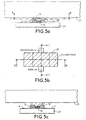
- FIGS. 5a to 5c are representative of a zoom of the bipolar transistor 11, embedded in the resin 71 to ensure the mechanical strength, the assembly being covered with a conductive film 81.
- the heat sink 31 is in contact with the conductive film 81.
- the power device / heat sink assembly step, the conductive film 81 makes it possible to perform the thermo-compression step without damaging the power device.
- the Figure 5b illustrates an AA sectional view of the transistor and the heat sink represented in FIG. Figure 5a .
- the input e corresponds to the basic contact
- the output s corresponds to the collector contact
- the mass m corresponds to the emitter contact.
- the Figure 5c illustrates a cross sectional view of the transistor and the heat sink.
- the heatsink assembly / electronic power device When the heatsink assembly / electronic power device is made, it comes to postpone said assembly at a support. According to two possible variants, either the conductive pillars are previously reported on the heat sink, or are reported on the support.
- the pillars may be an integral part of the metal element.
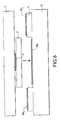
- the Figure 6 illustrates a step of embodiment of the invention schematizing the postponement of the preconstituted assembly on the support.
- This support comprises so-called low temperature solders B b1 , B b2 and B b3 , having lower melting temperatures than that used for the heat sink / power device assembly.
- the localized low temperature solder deposits compensate for differences in height and thus ensure simultaneous contact between the substrate bottom and the substrate and between the heat sink and the support via the pillars so as to constitute the encapsulated component.
- These low temperature solders generally have a high coefficient of expansion and allow thus damping mechanical variations (shear).
- the supply of material constituting the solder may advantageously be carried out by localized electrolytic growth which allows height control and a collective industrial process.
- the low temperature brazing heights may be of the order of a few tens of microns making it possible to compensate, in an extreme case, height variations of the electronic power device or the pillars.
- high temperature solders are characterized by good thermal conductivity, they are preferably placed closer to the heat source, in order to minimize heating.
- the pillars may be metal blocks with good copper thermal conductors, for example. These blocks can be made by electrolytic growth or assembly of elemental sheet.
- the heat sink may be diamond, copper, silver, gold, etc.
- the material constituting the support is a material having good heat conduction and having a coefficient of thermal expansion compatible with the material on which the heat is produced. component.
- the support may comprise microchannels mC in which circulates a cooling fluid.
- the support can be achieved by the stack of copper metal sheets, locally perforated, so as to circulate water inside the channels.
- the electronic power device is thus hermetically encapsulated.
- Brazing operations correspond to equivalent closure operations of the housing that can be carried out in a dehydrogenated atmosphere.
- the passage of the signals is advantageously carried out via via metallized elements made in the substrate of the device.
- power electronics as well as in the heat sink or in the support, depending on the nature of said heat sink and that of the support.
- the Figure 8 illustrates a variant of the invention in which the support is metallic and the heat sink is dielectric.
- the electrical signals are conveyed from the outside by metallic elements 311, pass through the heat sink 31, via V 311 conductive leads (the dotted lines shown in FIG. Figure 8 illustrate the path of the signals), to propagate along conductive elements 211, to an entry point E of the electronic power device 11.
- the signal is then recovered at the output S, is propagated along the conductive element 212, to pass through the heat sink via the conductive via 312, and to be recovered externally by the metal element 312.
- the mass M is in turn recovered from the power device via a via metal V 211 made in the substrate 21, and recovered at the metal support 51.
- the Figure 9 illustrates a variant of the invention in which the support 51 is dielectric, and the heat sink 31 is conductive.
- the electrical signals are introduced into the encapsulated component at the support 51, via conducting elements 511, 515, 512 and metal vias V 511 , V 512 to connect the input of the electronic power device by the intermediate via V 212 and conductive elements 211.
- the output S is recovered at a conductive element 212, a metal via V 213 through the substrate, then conductive elements 513, 516, 514 and metal vias V 513 and V 514 at the support 51.
- the mass M can be directly recovered at the heat sink which is conductive in this variant of the invention.
- the dielectric support may be covered with a metal layer.
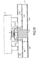
- the Figure 10 illustrates a variant close to the variant illustrated above, wherein the support 51 is made of dielectric material with incorporation of metal elements.
- the support 51 is a dielectric bilayer structure with metal tracks 516 and 517 inserted between the two layers. Typically, it may be alumina. The whole is drilled in its center, we introduce in the inclusion 52 a metal, so as to recover the mass at the support.
- the inputs and outputs of the electronic device are connected to the outside in the same way as described in Figure 9 .
- the mass is recovered by the metal inclusion 52 and conductive elements 518 and 519.
- the performances obtained of the component according to the invention were compared with those of components of the prior art, in the case of a power transistor comprising 40 fingers 100 ⁇ m long, the power dissipated in each finger being 576 mW. the substrate being GaAs 70 ⁇ m thick.
- the case a) relates to a transistor without massive thermal drain, the cases b), c) and d) concern components with thermal drain supported by the substrate and cases e), f), g), h) concern components according to the invention in which the heat sink rests at the level of the support.
Landscapes
- Cooling Or The Like Of Semiconductors Or Solid State Devices (AREA)
- Bipolar Transistors (AREA)
Claims (19)
- Verkapseltes elektronisches Bauteil, das einen ein Substrat (21) tragenden Träger (51) aufweist, wobei das Substrat eine elektronische Leistungsvorrichtung (11) enthält, dadurch gekennzeichnet, dass es eine Mikroabdeckung aufweist, die auf dem Träger (51) positionierte wärmeleitende Säulen (41) und einen Wärmeableiter (31) enthält, der die Fläche der Säulen und die Fläche der elektronischen Vorrichtung bedeckt.
- Elektronisches Bauteil nach Anspruch 1, dadurch gekennzeichnet, dass die elektronische Leistungsvorrichtung ein Transistor oder eine Gruppe von Transistoren vom Typ Stab oder Verstärker ist.
- Elektronisches Bauteil nach Anspruch 2, dadurch gekennzeichnet, dass der Transistor ein Bipolartransistor mit Heteroübergang ist.
- Elektronisches Bauteil nach einem der Ansprüche 2 oder 3, dadurch gekennzeichnet, dass die elektronische Leistungsvorrichtung (11) aus einer Stapelung von Schichten aus III-V-Materialien besteht.
- Elektronisches Bauteil nach einem der Ansprüche 1 bis 4, dadurch gekennzeichnet, dass der Träger (51) ein dielektrisches Material vom Typ Al2O3 oder AlN ist.
- Elektronisches Bauteil nach Anspruch 5, dadurch gekennzeichnet, dass der Träger (51) einen Zweischichtenaufbau aus dielektrischem Material mit Einfügung von Metallelementen in einer Ebene enthält, die sich in einer Tiefe h befindet, die bezüglich der unteren äußeren Ebene des Trägers definiert ist.
- Elektronisches Bauteil nach Anspruch 6, dadurch gekennzeichnet, dass es außerdem einen Einschluss (52) aus Metall über die ganze Höhe des Trägers (51) aufweist.
- Elektronisches Bauteil nach einem der Ansprüche 1 bis 4, dadurch gekennzeichnet, dass der Träger (51) ein gut wärmeleitendes Material ist, das einen mit dem Substrat kompatiblen Wärmeausdehnungskoeffizient hat.
- Elektronisches Bauteil nach einem der Ansprüche 1 bis 8, dadurch gekennzeichnet, dass es außerdem Einrichtungen für die Zirkulation eines Wärmeträgerfluids enthält, die in Höhe des Trägers integriert sind.
- Elektronisches Bauteil nach Anspruch 9, dadurch gekennzeichnet, dass der Träger aus einer Stapelung von stellenweise gelochten Folien besteht.
- Elektronisches Bauteil nach Anspruch 10, dadurch gekennzeichnet, dass die Zirkulationseinrichtungen Mikrokanäle sind.
- Elektronisches Bauteil nach einem der Ansprüche 1 bis 11, dadurch gekennzeichnet, dass der Wärmeableiter und/oder der Träger Lücken aufweisen, um die elektronische Leistungsvorrichtung elektrisch mit den Eingangs/Ausgangssignalen zu verbinden.
- Elektronisches Bauteil nach einem der Ansprüche 1 bis 12, dadurch gekennzeichnet, dass es Lötstellen enthält, die den Kontakt zwischen der elektronischen Vorrichtung und dem Wärmeableiter und/oder zwischen dem Substrat und dem Träger gewährleisten.
- Verfahren zur Herstellung eines verkapselten elektronischen Bauteils nach einem der Ansprüche 1 bis 13, dadurch gekennzeichnet, dass es die folgenden Schritte aufweist:- Herstellung der elektronischen Leistungsvorrichtung auf einem Substrat;- Montage des Wärmeableiters auf die Oberfläche der elektronischen Leistungsvorrichtung;- Übertragung der Anordnung auf die Oberfläche eines Trägers mittels leitender Säulen.
- Verfahren zur Herstellung eines elektronischen Bauteils nach Anspruch 14, dadurch gekennzeichnet, dass die elektronische Leistungsvorrichtung mit einem dicken Schutz vom Typ Metall bedeckt ist, und dass die Montage des Wärmeableiters auf die Oberfläche der elektronischen Leistungsvorrichtung durch Thermokompression erfolgt.
- Verfahren zur Herstellung eines elektronischen Bauteils nach Anspruch 14, dadurch gekennzeichnet, dass die Montage des Wärmeableiters auf die Oberfläche der elektronischen Leistungsvorrichtung mittels einer ersten Schweißlötstelle erfolgt.
- Verfahren zur Herstellung eines elektronischen Bauteils nach einem der Ansprüche 14 bis 16, dadurch gekennzeichnet, dass die Übertragung der Anordnung auf die Oberfläche einer Träger mittels zweiter Schweißlötstellen erfolgt.
- Verfahren zur Herstellung eines elektronischen Bauteils nach einem der Ansprüche 16 und 17, dadurch gekennzeichnet, dass die Schmelztemperatur der ersten Lötstelle höher als die Schmelztemperatur der zweiten Lötstellen ist.
- Verfahren zur Herstellung eines elektronischen Bauteils nach den Ansprüchen 16 bis 17, dadurch gekennzeichnet, dass die Lötvorgänge unter wasserstofffreier Atmosphäre durchgeführt werden.
Applications Claiming Priority (2)
| Application Number | Priority Date | Filing Date | Title |
|---|---|---|---|
| FR0109407 | 2001-07-13 | ||
| FR0109407A FR2827424B1 (fr) | 2001-07-13 | 2001-07-13 | Composant electronique encapsule comportant un dispositif electronique de puissance et procede de fabrication |
Publications (3)
| Publication Number | Publication Date |
|---|---|
| EP1276149A2 EP1276149A2 (de) | 2003-01-15 |
| EP1276149A3 EP1276149A3 (de) | 2007-05-30 |
| EP1276149B1 true EP1276149B1 (de) | 2010-01-27 |
Family
ID=8865514
Family Applications (1)
| Application Number | Title | Priority Date | Filing Date |
|---|---|---|---|
| EP02291698A Expired - Lifetime EP1276149B1 (de) | 2001-07-13 | 2002-07-05 | Eingekapseltes elektronisches Bauelement mit elektronischer Leitungsvorrichtung und Herstellungsverfahren |
Country Status (3)
| Country | Link |
|---|---|
| EP (1) | EP1276149B1 (de) |
| DE (1) | DE60235218D1 (de) |
| FR (1) | FR2827424B1 (de) |
Families Citing this family (2)
| Publication number | Priority date | Publication date | Assignee | Title |
|---|---|---|---|---|
| US7581585B2 (en) | 2004-10-29 | 2009-09-01 | 3M Innovative Properties Company | Variable position cooling apparatus |
| FR3069704B1 (fr) | 2017-07-27 | 2019-09-20 | Thales | Transistor a base metallique et comprenant des materiaux iii-v |
Family Cites Families (7)
| Publication number | Priority date | Publication date | Assignee | Title |
|---|---|---|---|---|
| FR2659494B1 (fr) * | 1990-03-09 | 1996-12-06 | Thomson Composants Microondes | Composant semiconducteur de puissance, dont la puce est montee a l'envers. |
| JPH05102262A (ja) * | 1991-10-03 | 1993-04-23 | Hitachi Ltd | 半導体装置及びそれを実装した実装装置 |
| US6028348A (en) * | 1993-11-30 | 2000-02-22 | Texas Instruments Incorporated | Low thermal impedance integrated circuit |
| US5734193A (en) * | 1994-01-24 | 1998-03-31 | The United States Of America As Represented By The Secretary Of The Air Force | Termal shunt stabilization of multiple part heterojunction bipolar transistors |
| DE19734509C2 (de) * | 1997-08-08 | 2002-11-07 | Infineon Technologies Ag | Leistungstransistorzelle |
| DE19735531A1 (de) * | 1997-08-16 | 1999-02-18 | Abb Research Ltd | Leistungshalbleitermodul mit in Submodulen integrierten Kühlern |
| FR2793953B1 (fr) * | 1999-05-21 | 2002-08-09 | Thomson Csf | Capacite thermique pour composant electronique fonctionnant en impulsions longues |
-
2001
- 2001-07-13 FR FR0109407A patent/FR2827424B1/fr not_active Expired - Fee Related
-
2002
- 2002-07-05 EP EP02291698A patent/EP1276149B1/de not_active Expired - Lifetime
- 2002-07-05 DE DE60235218T patent/DE60235218D1/de not_active Expired - Lifetime
Also Published As
| Publication number | Publication date |
|---|---|
| EP1276149A2 (de) | 2003-01-15 |
| DE60235218D1 (de) | 2010-03-18 |
| FR2827424B1 (fr) | 2005-02-18 |
| FR2827424A1 (fr) | 2003-01-17 |
| EP1276149A3 (de) | 2007-05-30 |
Similar Documents
| Publication | Publication Date | Title |
|---|---|---|
| EP0756322B1 (de) | Halbleiter mit integriertem Kühler | |
| FR2813440A1 (fr) | Dispositif a semiconducteur pour la commande d'energie electrique | |
| FR2710190A1 (fr) | Module pour dispositif à semi-conducteur à haute puissance avec une résistance thermique faible et une fabrication simplifiée. | |
| EP3154082B1 (de) | Verbesserte dbc-struktur, die mit einem trägerelement ausgestattet ist, in das ein material mit phasenumwandlung eingebaut ist | |
| FR2759493A1 (fr) | Dispositif de puissance a semiconducteur | |
| EP1276149B1 (de) | Eingekapseltes elektronisches Bauelement mit elektronischer Leitungsvorrichtung und Herstellungsverfahren | |
| WO2020021197A1 (fr) | Procede de fabrication d'un module electronique de puissance | |
| US5436497A (en) | Semiconductor device having a plurality of vertical type transistors having non-intersecting interconnections | |
| EP0446125B1 (de) | Leistungshalbleiteranordnung | |
| EP1110242B1 (de) | Thermische masse für langpuls-elektronikbauteile | |
| EP0085622B1 (de) | Montierungsträger für integriertes Schaltungsgehäuse mit Ausgangsleiter verteilt um die äussere Begrenzung des Gehäuses | |
| FR2565030A1 (fr) | Structure de metallisations de reprise de contacts d'un dispositif semi-conducteur et dispositif dote d'une telle structure | |
| FR2878077A1 (fr) | Composant electronique vertical autorefroidi | |
| FR2522875A1 (fr) | Dispositif servant a l'enregistrement ou a la reproduction d'images et dispositif semi-conducteur convenant a un tel dispositif | |
| FR2500215A1 (fr) | Dispositif de refroidissement d'un composant electronique de puissance, et composant encapsule dans un boitier muni d'un tel dispositif | |
| FR2761537A1 (fr) | Laser comprenant un empilement de diodes laser epitaxiees compris entre deux miroirs de bragg | |
| EP0067752B1 (de) | Thermische Kupplungszelle und mit solch einer Zelle ausgerüsteter temperaturgeregelter Raum | |
| FR2636777A1 (fr) | Dispositif semiconducteur a circuit de decharge de chaleur | |
| EP3242322B1 (de) | Elektronische leistungsvorrichtung mit flacher elektrischer verbindungsstruktur | |
| FR3112241A1 (fr) | Dispositif de refroidissement mis en œuvre dans une application d’électronique de puissance | |
| FR2726125A1 (fr) | Composant semiconducteur a transistors bipolaires, stabilises thermiquement | |
| EP2426712B1 (de) | Planares elektronisches Bauelement zur Leistungsumschaltung | |
| FR3051977A1 (fr) | Dispositif a haute mobilite electronique avec elements passifs integres | |
| EP0549405A1 (de) | Verfahren zum Verdrahten eines Laserarrays | |
| FR2868877A1 (fr) | Composants lasers a comportement thermique ameliore et procede de fabrication |
Legal Events
| Date | Code | Title | Description |
|---|---|---|---|
| PUAI | Public reference made under article 153(3) epc to a published international application that has entered the european phase |
Free format text: ORIGINAL CODE: 0009012 |
|
| AK | Designated contracting states |
Kind code of ref document: A2 Designated state(s): AT BE BG CH CY CZ DE DK EE ES FI FR GB GR IE IT LI LU MC NL PT SE SK TR |
|
| AX | Request for extension of the european patent |
Free format text: AL;LT;LV;MK;RO;SI |
|
| PUAL | Search report despatched |
Free format text: ORIGINAL CODE: 0009013 |
|
| AK | Designated contracting states |
Kind code of ref document: A3 Designated state(s): AT BE BG CH CY CZ DE DK EE ES FI FR GB GR IE IT LI LU MC NL PT SE SK TR |
|
| AX | Request for extension of the european patent |
Extension state: AL LT LV MK RO SI |
|
| 17P | Request for examination filed |
Effective date: 20071129 |
|
| AKX | Designation fees paid |
Designated state(s): DE FR GB IT NL |
|
| GRAP | Despatch of communication of intention to grant a patent |
Free format text: ORIGINAL CODE: EPIDOSNIGR1 |
|
| GRAS | Grant fee paid |
Free format text: ORIGINAL CODE: EPIDOSNIGR3 |
|
| GRAA | (expected) grant |
Free format text: ORIGINAL CODE: 0009210 |
|
| AK | Designated contracting states |
Kind code of ref document: B1 Designated state(s): DE FR GB IT NL |
|
| REG | Reference to a national code |
Ref country code: GB Ref legal event code: FG4D Free format text: NOT ENGLISH |
|
| REF | Corresponds to: |
Ref document number: 60235218 Country of ref document: DE Date of ref document: 20100318 Kind code of ref document: P |
|
| REG | Reference to a national code |
Ref country code: DE Ref legal event code: R096 Ref document number: 60235218 Country of ref document: DE Effective date: 20100318 |
|
| REG | Reference to a national code |
Ref country code: NL Ref legal event code: T3 |
|
| PLBE | No opposition filed within time limit |
Free format text: ORIGINAL CODE: 0009261 |
|
| STAA | Information on the status of an ep patent application or granted ep patent |
Free format text: STATUS: NO OPPOSITION FILED WITHIN TIME LIMIT |
|
| 26N | No opposition filed |
Effective date: 20101028 |
|
| REG | Reference to a national code |
Ref country code: DE Ref legal event code: R097 Ref document number: 60235218 Country of ref document: DE Effective date: 20101028 |
|
| REG | Reference to a national code |
Ref country code: FR Ref legal event code: PLFP Year of fee payment: 15 |
|
| REG | Reference to a national code |
Ref country code: FR Ref legal event code: PLFP Year of fee payment: 16 |
|
| REG | Reference to a national code |
Ref country code: FR Ref legal event code: PLFP Year of fee payment: 17 |
|
| PGFP | Annual fee paid to national office [announced via postgrant information from national office to epo] |
Ref country code: FR Payment date: 20210624 Year of fee payment: 20 Ref country code: IT Payment date: 20210628 Year of fee payment: 20 |
|
| PGFP | Annual fee paid to national office [announced via postgrant information from national office to epo] |
Ref country code: NL Payment date: 20210716 Year of fee payment: 20 Ref country code: GB Payment date: 20210623 Year of fee payment: 20 |
|
| PGFP | Annual fee paid to national office [announced via postgrant information from national office to epo] |
Ref country code: DE Payment date: 20210622 Year of fee payment: 20 |
|
| REG | Reference to a national code |
Ref country code: DE Ref legal event code: R071 Ref document number: 60235218 Country of ref document: DE |
|
| REG | Reference to a national code |
Ref country code: NL Ref legal event code: MK Effective date: 20220704 |
|
| REG | Reference to a national code |
Ref country code: GB Ref legal event code: PE20 Expiry date: 20220704 |
|
| PG25 | Lapsed in a contracting state [announced via postgrant information from national office to epo] |
Ref country code: GB Free format text: LAPSE BECAUSE OF EXPIRATION OF PROTECTION Effective date: 20220704 |
|
| P01 | Opt-out of the competence of the unified patent court (upc) registered |
Effective date: 20230517 |