EP1276168A1 - Irreversibles schaltungsmodul - Google Patents
Irreversibles schaltungsmodul Download PDFInfo
- Publication number
- EP1276168A1 EP1276168A1 EP01919814A EP01919814A EP1276168A1 EP 1276168 A1 EP1276168 A1 EP 1276168A1 EP 01919814 A EP01919814 A EP 01919814A EP 01919814 A EP01919814 A EP 01919814A EP 1276168 A1 EP1276168 A1 EP 1276168A1
- Authority
- EP
- European Patent Office
- Prior art keywords
- laminate
- transmission line
- circuit module
- reciprocal circuit
- module according
- Prior art date
- Legal status (The legal status is an assumption and is not a legal conclusion. Google has not performed a legal analysis and makes no representation as to the accuracy of the status listed.)
- Withdrawn
Links
- 230000002427 irreversible effect Effects 0.000 title abstract 2
- 230000005540 biological transmission Effects 0.000 claims abstract description 100
- 239000004020 conductor Substances 0.000 claims abstract description 93
- 239000003990 capacitor Substances 0.000 claims abstract description 77
- 230000008878 coupling Effects 0.000 claims description 33
- 238000010168 coupling process Methods 0.000 claims description 33
- 238000005859 coupling reaction Methods 0.000 claims description 33
- 238000003475 lamination Methods 0.000 claims description 12
- 239000011148 porous material Substances 0.000 claims description 12
- 229910052802 copper Inorganic materials 0.000 claims description 5
- 239000010949 copper Substances 0.000 claims description 5
- RYGMFSIKBFXOCR-UHFFFAOYSA-N Copper Chemical compound [Cu] RYGMFSIKBFXOCR-UHFFFAOYSA-N 0.000 claims description 4
- 239000010410 layer Substances 0.000 description 45
- 238000003780 insertion Methods 0.000 description 12
- 230000037431 insertion Effects 0.000 description 12
- 239000011347 resin Substances 0.000 description 10
- 229920005989 resin Polymers 0.000 description 10
- 238000002955 isolation Methods 0.000 description 9
- 239000002223 garnet Substances 0.000 description 7
- 238000004891 communication Methods 0.000 description 4
- 239000003989 dielectric material Substances 0.000 description 4
- 230000000694 effects Effects 0.000 description 4
- 229910052751 metal Inorganic materials 0.000 description 4
- 239000002184 metal Substances 0.000 description 4
- 239000000470 constituent Substances 0.000 description 3
- 230000006866 deterioration Effects 0.000 description 3
- 238000004519 manufacturing process Methods 0.000 description 3
- 238000000034 method Methods 0.000 description 3
- 230000003071 parasitic effect Effects 0.000 description 3
- 238000007639 printing Methods 0.000 description 3
- 238000005245 sintering Methods 0.000 description 3
- JBRZTFJDHDCESZ-UHFFFAOYSA-N AsGa Chemical compound [As]#[Ga] JBRZTFJDHDCESZ-UHFFFAOYSA-N 0.000 description 2
- 229910001218 Gallium arsenide Inorganic materials 0.000 description 2
- 230000001413 cellular effect Effects 0.000 description 2
- 230000007423 decrease Effects 0.000 description 2
- 230000003247 decreasing effect Effects 0.000 description 2
- 238000007606 doctor blade method Methods 0.000 description 2
- 238000005516 engineering process Methods 0.000 description 2
- 230000009467 reduction Effects 0.000 description 2
- 229910010293 ceramic material Inorganic materials 0.000 description 1
- 230000001276 controlling effect Effects 0.000 description 1
- 238000010586 diagram Methods 0.000 description 1
- 230000005669 field effect Effects 0.000 description 1
- 239000010408 film Substances 0.000 description 1
- 230000006872 improvement Effects 0.000 description 1
- 238000009413 insulation Methods 0.000 description 1
- 239000011229 interlayer Substances 0.000 description 1
- 238000010030 laminating Methods 0.000 description 1
- 230000007257 malfunction Effects 0.000 description 1
- 239000000463 material Substances 0.000 description 1
- 238000010295 mobile communication Methods 0.000 description 1
- 230000001105 regulatory effect Effects 0.000 description 1
- 229910052709 silver Inorganic materials 0.000 description 1
- 238000005476 soldering Methods 0.000 description 1
- 230000000087 stabilizing effect Effects 0.000 description 1
- 239000010409 thin film Substances 0.000 description 1
- 238000009966 trimming Methods 0.000 description 1
- 238000004804 winding Methods 0.000 description 1
Images




Classifications
-
- H—ELECTRICITY
- H01—ELECTRIC ELEMENTS
- H01P—WAVEGUIDES; RESONATORS, LINES, OR OTHER DEVICES OF THE WAVEGUIDE TYPE
- H01P1/00—Auxiliary devices
- H01P1/32—Non-reciprocal transmission devices
- H01P1/38—Circulators
- H01P1/383—Junction circulators, e.g. Y-circulators
-
- H—ELECTRICITY
- H01—ELECTRIC ELEMENTS
- H01P—WAVEGUIDES; RESONATORS, LINES, OR OTHER DEVICES OF THE WAVEGUIDE TYPE
- H01P1/00—Auxiliary devices
- H01P1/32—Non-reciprocal transmission devices
- H01P1/38—Circulators
- H01P1/383—Junction circulators, e.g. Y-circulators
- H01P1/387—Strip line circulators
Definitions
- the present invention relates to a non-reciprocal circuit module such as a circulator, an isolator, etc. used in a microwave communications equipment, etc. such as a mobile phone, etc.
- a non-reciprocal circuit module such as a circulator, an isolator, etc. used in a microwave communications equipment, etc. such as a mobile phone, etc.
- Wireless communications devices for instance, mobile phones have become popular remarkably in recent years with their functions and services improved increasingly.
- a mobile phone there are various systems for mobile phones, for instance, EGSM (extended global system for mobile communications) and DCS1800 (digital cellular system 1800) systems widely used mostly in Europe, a PCS (personal communications services) system used in the U. S., and a PDC (personal digital cellular) system used in Japan.
- EGSM extended global system for mobile communications
- DCS1800 digital cellular system 1800
- PCS personal communications services
- PDC personal digital cellular
- a high-frequency signal from a modulation circuit (not shown) is amplified by an amplifier 1, and an output proportional to the high-frequency signal is taken out by a directional coupler 2 and supplied to an automatic gain control circuit 7 to control the output power of the amplifier 1.
- a non-reciprocal circuit device (isolator) 3 placed on the downstream side of the directional coupler 2 prevents a reflected wave generated by the mismatching, etc. of characteristic impedance and line impedance in each part (an antenna 6, a low-pass filter 4 and a duplexer 5) from entering into the amplifier 1.
- Fig. 19 is an exploded perspective view showing a conventional non-reciprocal circuit device.
- This non-reciprocal circuit device comprises a central conductor assembly 10, a resin case 12, dielectric bodies 50a, 50b, 50c constituting load capacitors, a permanent magnet 9, and metal cases 7, 8.
- the central conductor assembly 10 comprises an integral central conductor member constituted by a ground electrode formed by a thin copper plate and central conductors 14a, 14b, 14c radially extending therefrom in three directions, and a disc-shaped garnet (magnetic body) 13, the central conductor member encircling the disc-shaped garnet (magnetic body) 13, and the central conductors 14a, 14b, 14c being folded and crossing at 120° with mutual insulation at a center on the upper surface of the garnet (magnetic body) 13.
- the central conductor assembly 10 is placed in a recess 15 substantially at a center of the resin case 12, and the dielectric bodies 50a, 50b, 50c are placed in three rectangular recesses around the recess 15.
- the ground electrode of the central conductor member is soldered to a ground plate of the resin case 12, and the central conductors 14a, 14b, 14c (input/output electrodes) of the central conductor member are soldered to external electrodes of the dielectric bodies 50a, 50b, 50c on their upper surfaces.
- the permanent magnet 9 for applying a DC magnetic field to the central conductors 14a, 14b, 14c on the garnet 13 is placed above the central conductor assembly 10.
- mobile phone having such a structure comprises a transmitting circuit means, into which the directional coupler 2, coupling capacitors, the non-reciprocal circuit device 3 and the low-pass filter 4 are incorporated as separate parts, there arise disadvantages described below.
- the non-reciprocal circuit device 3 is tried to be miniaturized simply by the miniaturization of the central conductor assembly 10 and the dielectric bodies 50a, 50b, 50c, there would arise the following problems: If the central conductor assembly 10 is miniaturized, the non-reciprocal circuit device deviates from the optimally operable size as a magnetic body. In addition, if a dielectric material having a high dielectric constant is used to miniaturize the dielectric body, loss by the dielectric material increases relatively, resulting in deterioration in electric characteristics as the non-reciprocal circuit device.
- the directional coupler 2 suffers from an insertion loss, which mainly comprises coupling loss and conductor loss, and the non-reciprocal circuit device 3 and the low-pass filter 4 have insertion loss. Accordingly, when they are used as separate parts, the loss of each part is accumulated, resulting in large loss in the overall transmitting circuit means. Loss in the transmitting circuit means leads to increase in power consumption, and this loss is not ignorable for mobile phones having limited battery capacities.
- Japanese Patent Laid-Open No. 9-270608 proposes that output in proportion to a high-frequency signal is taken out from a capacitor (output-detecting capacitance) branched from the input terminal of an isolator, that the output is supplied to an automatic gain control circuit to control the output power of an amplifier, and that the output-detecting capacitor is formed in an integral laminate constituted by laminating dielectric sheets together with load capacitors of the isolator.
- the output-detecting capacitance when used, sufficient directivity cannot be obtained due to the influence of parasitic capacitance. Therefore, unless an output-detecting capacitor designed by taking interference between electrode patterns into sufficient consideration is formed in the laminate, the desired coupling would not be obtained.
- the output-detecting capacitance should be as small as 0.15 pF, resulting in difficulty in control, and large variation in the coupling due to unevenness in production and parasitic capacitance.
- the interference between electrode patterns makes further miniaturization substantially difficult.
- an object of the present invention is to provide a non-reciprocal circuit module having the functions of a non-reciprocal circuit device and a directional coupler to suppress the number and area of parts mounted and production cost.
- Another object of the present invention is to provide a non-reciprocal circuit module with small loss and further provided with the function of a low-pass filter.
- a further object of the present invention is to provide a non-reciprocal circuit module provided with a high-frequency power amplifier.
- the first non-reciprocal circuit module of the present invention comprises (a) a permanent magnet for applying a DC magnetic field to a magnetic body, (b) an assembly comprising a plurality of central conductors and the magnetic body placed therein, each of the central conductors having a common terminal at one end and an input/output terminal for a high-frequency signal at the other end, (c) a plurality of load capacitors formed in a laminate constituted by a plurality of dielectric layers having conductor layers and connected to the central conductor, (d) a first transmission line connected to any one of the central conductors, and (e) a second transmission line magnetically coupled to the first transmission line, the first transmission line and the second transmission line being formed in the laminate.
- a high-frequency signal from an amplifier is supplied to the terminal P1 of the first transmission line formed in the laminate.
- the second transmission line is formed in the laminate such that it is magnetically coupled to the first transmission line.
- part of the high-frequency signal appears on the second transmission line, whereby high-frequency electric power in proportion to the high-frequency signal is supplied from a terminal P5 formed in the non-reciprocal circuit module to the automatic gain control circuit.
- the high-frequency signal is transmitted to the terminal P2 and then supplied to the non-reciprocal circuit device.
- the high-frequency signal supplied through the terminal P2 is transmitted to the garnet via the central conductor in the assembly, in which the traveling direction of the high-frequency signal is turned by 120° under the function of a DC magnetic field applied from the permanent magnet to the garnet.
- the high-frequency signal is transmitted to the central conductor connected to the terminal P3, from which it is output.
- the first and second transmission lines cooperating to constitute the directional coupler are formed as laminate constituents in the laminate constituted by a plurality of dielectric layers having conductor layers, together with a plurality of load capacitors constituting the non-reciprocal circuit device. With this structure, impedance matching between the non-reciprocal circuit device and the directional coupler can easily be achieved.
- the impedance of the directional coupler is determined by the width of a transmission line constituting the directional coupler, and its distance from the ground surface, etc.
- the impedance of the non-reciprocal circuit device is determined by the materials and shapes of the magnetic body and the central conductors constituting the central conductor assembly, and the magnetic force of the permanent magnet.
- the characteristic impedance of the directional coupler and the non-reciprocal circuit device is generally set at 50 ⁇ , it inevitably varies to some extent when the directional coupler and the non-reciprocal circuit device are constituted as separate devices, due to inevitable unevenness in production, for instance, unevenness in the thickness of the dielectric layer, the line width of the transmission line, the magnetic force of the magnetic body, etc.
- the non-reciprocal circuit module can be miniaturized.
- the second non-reciprocal circuit module of the present invention comprises (a) a permanent magnet for applying a DC magnetic field to a magnetic body, (b) an assembly comprising a plurality of central conductors and the magnetic body placed therein, each of the central conductors having a common terminal at one end and an input/output terminal for a high-frequency signal at the other end, and (c) a laminate comprising a plurality of load capacitors formed by conductor layers electrically connected to the assembly and each opposing via a dielectric layer, a first transmission line connected to any one of the central conductors, and a second transmission line magnetically coupled to the first transmission line, the conductor layers on the hot side and the ground side for the plural load capacitors being divided for every load capacitor.
- This non-reciprocal circuit module exhibits the same effects as the first non-reciprocal circuit module, and has low loss with the conductor layers on the hot side and the ground side for the plural load capacitors divided for every load capacitor, thereby preventing the inductance parasitic to the load capacitors and equivalent series resistance from increasing to keep the load capacitor at a high Q value (low loss).
- the laminate has a pore for receiving the assembly substantially at center.
- This pore may be a through-hole or a recess.
- the third non-reciprocal circuit module of the present invention comprises (a) a permanent magnet for applying a DC magnetic field to a plate-shaped magnetic body, (b) an assembly comprising a central conductor member having central conductors extending from a ground electrode formed by a thin copper plate radially in a plurality of directions, and the magnetic body, the central conductors encircling the magnetic body in a mutually insulated manner and crossing substantially at the center of the magnetic body, and (c) a laminate constituted by a plurality of dielectric layers having conductor layers and having a pore for receiving the assembly substantially at center, the laminate comprising a plurality of load capacitors each formed by conductor layers opposing via the dielectric layer around the pore, a first transmission line connected to any one of the central conductors, and a second transmission line magnetically coupled to the first transmission line, the load capacitors being electrically connected to the assembly, such that one of the load capacitors is electrically connected to the first transmission line via the central conductor, while the other load capacitors
- such a structure makes it possible to separately confirm the electric characteristics of the non-reciprocal circuit and the directional coupler. Accordingly, when electric troubles take place in the non-reciprocal circuit module, it is possible to easily identify which functioning parts are culprits.
- an electrostatic capacitor is connected to at least one end of the first transmission line in parallel with the load capacitor to constitute the low-pass filter. It is also preferable that an electrostatic capacitor is connected in parallel to the first transmission line to constitute a parallel resonance circuit, and that an attenuation pole is provided at a resonance frequency of the parallel resonance circuit.
- each load capacitor is preferably constituted by conductor layers opposing via a dielectric layer in a lamination direction, part of the conductor layers being formed on a main surface of the laminate opposing to the permanent magnet.
- the first and second transmission lines constituting the directional coupler are opposing via a dielectric layer in a lamination direction.
- Such a structure needs smaller planar area than when the directional coupler is constituted by placing two transmission lines on the same plane.
- winding the transmission line in a coil shape can preferably prevent the variation of coupling by positional deviation at the time of lamination.
- the first and/or second transmission line may be constituted by electrically connecting a plurality of conductor layers formed on the different dielectric layers via through-holes.
- the coupling of the directional coupler can be controlled by adjusting the overlapping area of the conductor layers for the first and second transmission lines opposing via a dielectric layer in a lamination direction.
- a wide ground electrode formed by a conductor layer, and the ground electrode serves as a common ground for the first and second transmission lines and the load capacitors.
- conductor layers constituting the first and second transmission lines are formed in a first laminate region, while a plurality of load capacitors constituting the non-reciprocal circuit are formed in a second laminate region different from the first laminate region.
- the first and second transmission lines may be placed such that they do not overlap conductor layers constituting the load capacitor in a lamination direction, or the first laminate region may be separated from the second laminate region by the ground electrode.
- the high-frequency amplifier can be mounted onto the laminate.
- the output terminal of the high-frequency amplifier is connected to one end of the first transmission line by conductor layers in the laminate.
- the high-frequency amplifier comprises an amplifier circuit having a transistor, an input-matching circuit connected to the input terminal of the amplifier circuit, and an output-matching circuit connected to the output terminal of the amplifier circuit, the input-matching circuit and the output-matching circuit each having a capacitor and an inductor.
- the transistor of the amplifier circuit is mounted onto the laminate, while the inductor is formed as a transmission line in the laminate.
- the capacitor is preferably formed by capacitor electrodes opposing via a dielectric layer in the laminate.
- the transistor of the amplifier circuit is preferably a field effect transistor, and the high-frequency amplifier is preferably constituted by a transistor made of gallium arsenide GaAs, these parts being mounted onto the laminate.
- the characteristic impedance of the non-reciprocal circuit is set at 50 ⁇ , while the input/output impedance of the transistor is about several ⁇ to several tens of ⁇ , needing input/output-matching circuits for connection therebetween.
- a low-pass filter is used as an output-matching circuit connected to the output terminal of the amplifier circuit as shown in the equivalent circuit of Fig. 17, the number of circuit elements can be reduced as compared with when the output-matching circuit is mounted separately, resulting in improvement in the insertion loss characteristics.
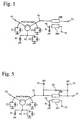
- Fig. 1 shows an equivalent circuit of the non-reciprocal circuit module according to one embodiment of the present invention
- Fig. 2 shows the non-reciprocal circuit module according to one embodiment of the present invention
- Fig. 3 shows the circuit structure of each layer constituting the laminate of the non-reciprocal circuit module of the present invention.
- This non-reciprocal circuit module is provided with the functions of a non-reciprocal circuit and a directional coupler, and operated at the desired impedance Z 0 with an external magnetic field applied from a permanent magnet 9 to a magnetic body 13 in the non-reciprocal circuit portion.
- load capacitors C1 connected between terminals P2, P3, P4 and a ground GND determine the operation frequency of the non-reciprocal circuit.
- the inductance L of the magnetic body 13 encircled by central conductors 14a, 14b and 14c varies by an external magnetic field from the permanent magnet 9.
- a resistor Ri is connected between the terminal P4 and the ground.
- a directional coupler is constituted by a first transmission line 200 placed between the terminal P2 and the terminal P1, and a second transmission line 201 opposing the first transmission line 200 with magnetic coupling and having a terminal P6 connected to a resistor Rc.
- the load capacitors C1 and the first and second transmission lines 200, 201 are formed as laminate constituents by conductor layers placed in the laminate 11 on a resin base 12, and resistors Ri, Rc constituted by printed resistors, chip resistor elements, etc. are placed on the laminate 11.
- the laminate 11 is made of a low-temperature-sinterable, dielectric ceramic material, for instance, a dielectric material having a specific dielectric constant ⁇ r of about 8 and sinterable at 900°C.
- the laminate 11 may be produced, for instance, by forming green sheets each having a thickness of 30-100 ⁇ m by a doctor blade method, printing each green sheet with a conductive paste based on a conductor such as Ag, Cu, etc. to form the first and second transmission lines 200, 201 for the directional coupler and electrodes (conductor layers) for constituting load capacitors for the non-reciprocal circuit, integrally transmission a plurality of conductor-printed green sheets, and sintering the resultant laminate.
- An assembly 10 comprises a central conductor member comprising three central conductors 14a, 14b, 14c integrally radially extending from a ground electrode formed by, for instance, a thin copper plate, and a magnetic body 13 such as a disc-shaped garnet, etc. placed on the ground electrode of the central conductor member.
- the central conductors 14a, 14b, 14c are bent along a side surface of the disc-shaped magnetic body 13, and overlapped each other at a distance of 120° in a mutually insulated manner via an insulating film, etc.
- the assembly 10 is placed in a center pore 15 of the laminate 11.
- One end of the central conductor 14a is connected to an electrode 50a for constituting a load capacitor on an upper surface of the laminate 11, and a central conductor 14b is connected to an electrode 50b.
- One end of the central conductor is connected to an electrode 50c on an upper surface of the laminate 11, and the other end of each central conductor is connected to a ground electrode (conductor plate) 18 on the resin base 12 via a ground electrode positioning on a lower surface of the disc-shaped magnetic body 13.
- the side surface of the resin base 12 is provided with a plurality of external terminals 17a-17f for connecting to a mounting board.
- a sheet-shaped magnetic body may be formed by a sheet-forming technology such as a doctor blade method, etc., and formed with an electrode pattern for a central conductor and integrally laminated and then sintered.
- a central conductor may be formed on a sintered magnetic body by a thin-film technology.
- the non-reciprocal circuit module of the present invention can be obtained.
- the laminate 11 is used for a non-reciprocal circuit module for W-CDMA (wideband CDMA, transmitted frequency TX: 1.92 GHz-1.98 GHz).
- W-CDMA wideband CDMA, transmitted frequency TX: 1.92 GHz-1.98 GHz.
- W-CDMA is taken as an example of a system for a wireless communications device, the same effects of the present invention can be obtained in the other systems.
- the lowermost green sheet 112 is formed with a ground electrode 63 substantially on an entire rear surface, and then with electrodes 80a-80c, which are connected to connection electrodes 30a-30c formed on a resin base 12.
- a green sheet 109 provided with a line electrode 73 for constituting a first transmission line is laminated thereon.
- a green sheet 108 formed with a through-hole electrode shown by a black circle in the figure
- a green sheet 107 formed with a line electrode 72 for constituting the second transmission line and a through-hole electrode One end of the line electrode 72 is connected to an external electrode 19c formed on the side surface of the laminate 11, and one end of the line electrode 73 is connected to an external electrode 19a formed on the side surface of the laminate 11.
- a connection electrode 70 formed on the green sheet 106 has one end connected to a line electrode 73 via a through-hole electrode, and the other end connected to a pattern electrode 50d on an upper surface of the laminate 11 via through-hole electrodes of green sheets 100-105.
- a line electrode 72 is connected to a pattern electrode 50e on an upper surface of the laminate 11 via through-hole electrodes formed in the green sheets 100-106.
- Laminated on the green sheet 106 are a green sheet 105 provided with a ground electrode 62 and through-hole electrodes, a green sheet 104 provided with electrode patterns 52a-52c for load capacitors and through-hole electrodes, a green sheet 103 provided with a ground electrode 61 and through-hole electrodes, a green sheet 102 provided with electrode patterns 51a-51c for load capacitors and through-hole electrodes, a green sheet 101 provided with a ground electrode 60 and through-hole electrodes, and a green sheet 100 provided with electrode patterns 50a-50c for load capacitors, connecting electrodes 50d-50f and through-hole electrodes in this order.
- Load capacitors C1 connected to terminals P3, P2 and P4, respectively are constituted by electrode patterns 50b, 51b, 52b, electrode patterns 50c, 51c, 52c and electrode patterns 50a, 51a, 52a, and ground electrodes 60, 61, 62.
- Resistors Ri, Rc are formed on an upper surface of the laminate 11 by a printing/baking method.
- the resistor Ri is a terminal resistor for an isolator
- the resistor Rc is a terminal resistor for a directional coupler.
- chip resistors may be used, and each resistor may be formed simultaneously with sintering the laminate.
- input/output electrodes 80a, 80b, 80c connected to connection electrodes 30a, 30b, 30c of the resin base 12, and a ground electrode 63 connected to a ground electrode 18 of the resin base 12.
- a dielectric material having a specific dielectric constant ⁇ r of about 8 is used to form the laminate 11, with a distance of 300 ⁇ m between the upper and lower ground electrodes sandwiching the line electrodes, each line electrode having a width of 100 ⁇ m and a line length of about 1/16 wavelength.
- the line electrodes 72, 73 constituting the first and second transmission lines respectively have a one-turn-coil shape, opposing at a distance of 100 ⁇ m via a dielectric layer in a lamination direction to have the coupling of 20 dB. It is preferable that with a directional coupler having such a coil coupling structure, the coupling can easily be controlled by the layer distance between the main line and the sub-line and the line length of their overlapping portion.
- the line electrodes may be turned by one or more times depending on the shape of the laminate 11.
- line electrodes for the directional coupler and electrodes for the load capacitors are formed on separate layers of the laminate with a ground electrode sandwiched therebetween to have decreased interference of these parts.
- the first transmission line (line electrode 73) for the directional coupler and an electrode pattern 50b for the load capacitor are connected on an outer surface of the laminate 11, so that the electric characteristics of the non-reciprocal circuit and the directional coupler can separately be confirmed.
- This makes it possible to easily identify which functional parts are culprits when there are electric malfunctions in the non-reciprocal circuit. For instance, even if a center frequency deviates in the non-reciprocal circuit, such deviation can easily be found.
- electrodes 50a, 50b, 50c for load capacitors formed on an outer surface of the laminate 11 are trimmed to adjust their capacitance, the center frequency can be varied.
- the laminate 11 having an outer size of 4 mm x 3.5 mm x 0.5 mm was obtained.
- an extremely small non-reciprocal circuit module having an equivalent circuit shown in Fig. 1, a structure shown in Fig. 2 and an outer size of 4 mm x 4 mm x 1.7 mm was produced.
- Figs. 4(a)-(c) show the insertion loss characteristics and coupling characteristics (degree of coupling) of this non-reciprocal circuit module, as well as its isolation characteristics between the output terminal P3 and the input terminal P1.
- the non-reciprocal circuit module of this example has excellent insertion loss characteristics, coupling characteristics and isolation characteristics in a desired frequency band with directivity of 18 dB or more. This indicates that the non-reciprocal circuit module of this example is fully small and high in performance.
- Fig. 5 shows an equivalent circuit of the non-reciprocal circuit module according to another embodiment of the present invention.
- This non-reciprocal circuit module is provided with the function of a directional coupler as well as the function of a low-pass filter.
- Example 1 Because the non-reciprocal circuit module of this example has the same portions as those of Example 1, only different portions are explained here. The differences from Example 1 are; (1) the first and second electrostatic capacitors C3, C4 are connected between both ends of the first transmission line and the ground to constitute a low-pass filter by the first transmission line and the first and second electrostatic capacitors C3, C4, and (2) the third electrostatic capacitor C2 is connected in parallel to the first transmission line to have sharp attenuation.
- Fig. 6 is an exploded perspective view showing the laminate 11 of this example.
- the differences from Example 1 are that an electrode 300 for an electrostatic capacitor C3 is formed on the green sheet 106, that an electrode 400 for an electrostatic capacitor C2 is formed on the green sheet 110, that an electrode 401 for an electrostatic capacitor C2 is formed on the green sheet 111, and that an electrode 301 for an electrostatic capacitor C4 is formed on the green sheet 112.
- the first transmission line 200 can be utilized as an inductor for the low-pass filter, but also the non-reciprocal circuit module can be made multi-functional while maintaining the insertion loss and the size at the same level as Example 1 as compared with when the low-pass filter is simply added to the non-reciprocal circuit module of Example 1. Accordingly, further reduction of the number of parts and decrease in the mounting area can be achieved.
- the line electrode 73 constituting the first transmission line 200 needs only be elongated properly while keeping the opposing relation with the second transmission line 201 to provide the first distributed constant line 200 with inductance as shown in Fig. 8.
- Figs. 7(a)-(c) show the insertion loss characteristics and coupling characteristics of this non-reciprocal circuit module as well as its isolation characteristics between the output terminal P3 and the input terminal P1.
- excellent insertion loss characteristics, coupling characteristics and isolation characteristics are obtained in the desired frequency band, and the second harmonic attenuation is 30 dB or more with directivity of 19 dB or more. This indicates that the non-reciprocal circuit module of this example is sufficiently small and high in performance.
- Examples 1, 2 are directed to the non-reciprocal circuit module for W-CDMA, this example is directed to a non-reciprocal circuit module for D-AMPS (digital-advanced mobile phone service, transmitted frequency TX: 824 MHz-849 MHz).
- D-AMPS digital-advanced mobile phone service, transmitted frequency TX: 824 MHz-849 MHz.
- any of the inductance, load capacitance and line length of a directional coupler should be increased, resulting in difficulty in the miniaturization.
- part of a circular pore 16 of the laminate 11 in this example is buried as shown in Fig. 9.
- This provides advantages of increasing the area of an electrode pattern on the green sheet and the capacitance of the load capacitor C1, thereby stabilizing the ground. Therefore, the magnetic body 13 has a deformed circular shape of 2.5 mm in diameter partially cut by 0.75 mm from a periphery in this Example.
- the internal structure of the laminate 11 is explained in a lamination order referring to Fig. 10.
- the lowermost green sheet 112 is provided with a ground electrode 63 and a pattern electrode connected to a connection electrode formed on the resin base 12 substantially on an entire rear surface.
- One line electrode 73b constituting the second transmission line is formed on the green sheet 112.
- a green sheet 111 formed with another line electrode 73a constituting the second transmission line is laminated on the green sheet 112.
- the green sheet 111 is provided with a through-hole electrode, through which the line electrode 73a is connected to the line electrode 73b, thereby constituting a second transmission line in a one-turn shape.
- Laminated on the green sheet 111 are a green sheet 110 on which an electrode pattern is not printed, and a green sheet 109 formed with a line electrode 72b constituting the first transmission line.
- a green sheet 108 formed with another line electrode 72a constituting the first transmission line is laminated on the green sheet 109.
- the green sheet 108 is provided with a through-hole electrode, through which the line electrode 72a is connected to the line electrode 72b, thereby constituting a first transmission line in a one-turn shape.
- One end of this first transmission line extends to a pattern electrode 50d on an upper surface of the laminate 11 through the through-hole electrodes formed in the green sheets 100-107.
- green sheets 107and 106 both provided with through-hole electrodes, a green sheet 105 provided with a ground electrode 62 and through-hole electrodes, a green sheet 104 provided with electrode patterns 52a-52c for load capacitors and through-hole electrodes, a green sheet 103 provided with a ground electrode 61 and through-hole electrodes, a green sheet 102 provided with electrode patterns 51a-51c for load capacitors and through-hole electrodes, a green sheet 101 provided with a ground electrode 60 and through-hole electrodes, and a green sheet 100 provided with electrode patterns 50a-50c for load capacitors, connecting pattern electrodes 50d, 50f and through-hole electrodes in this order.
- Load capacitors C1 connected to terminals P2, P3 and P4 are constituted by electrode patterns 50b, 51b, 52b, electrode patterns 50c, 51c, 52c and electrode patterns 50a, 51a, 52a, and ground electrode patterns 60, 61, 62.
- a resistor Ri is formed as a terminal resistor for an isolator on an upper surface of the laminate 8 by a printing/baking method.
- a chip resistor may be used in place of the printed resistor, and the resistor Ri may be formed by simultaneously with sintering the laminate.
- a laminate 11 having an outer size of 4 mm x 3.5 mm x 0.5 mm.
- the first transmission line and the second transmission line are placed such that they enclose a pore 16.
- relatively long lines can be formed in a restricted region in the laminate 11. It has thus been found that a distributed constant line can be formed with a line length with only small unevenness in the degree of coupling in a frequency band of a transmitting signal, and that directivity, one of the important characteristics of the directional coupler, is 10 dB or more.
- a dielectric body having a specific dielectric constant ⁇ r of about 8 is used to constitute the laminate 11, with a distance of 400 ⁇ m between the ground electrodes 62, 63 sandwiching the first and second transmission lines, each line electrode having a width of 100 ⁇ m, and the first and second transmission lines having a line length of about 1/12 wavelength.
- the first and second transmission 200, 201 are each in a one-turn coil type, and the closest electrode patterns 72b, 73a among those for the first and second distributed constant lines opposing via a dielectric layer oppose each other by a distance of 100 ⁇ m.
- the coupling of 14.3 dB has been achieved.
- Such a coil coupling structure is preferable, because the degree of coupling can easily be controlled by a layer distance between the main line and the sub-line and a line length of their overlapping portion.
- the line electrodes may be turned one or more times depending on the shape of the laminate 11.
- Fig. 12 is a plan view showing green sheets 108, 109 provided with line electrodes 72a, 72b for constituting the first transmission line 200.
- the first transmission line 200 of this example has line electrodes 72a, 72b formed on two layers and connected via through-hole electrodes as in Example 3. With the positions of through-hole electrodes and the length of line electrodes 72a, 72b properly varied, an area was changed in the closest electrode patterns among those of the first and second transmission lines opposing via a dielectric layer.
- the through-hole electrode is at a point A, B, C or D on the green sheet 108 shown in Fig. 12, it is in contact with a portion at the point A, B, C or D on the green sheet 109.
- a through-hole electrode is formed in a portion B in Example 3.
- the degree of coupling varies from 12.5 dB to 14.3 dB, 14.8 dB and 15.0 dB at each point A-D.
- the degree of coupling can easily be controlled only by adjusting the position of a through-hole in a plane.
- the position of the through-hole electrode in the first transmission line 200 is changed to vary the degree of coupling in this example, the same effects are also obtained by changing the position of a through-hole electrode in the second transmission line 201 or the positions of through-hole electrodes in both first and second distributed constant lines.
- the directivity was 10 dB or more, on the same level as in Example 3.
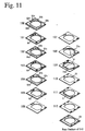
- FIG. 11 A further example of the non-reciprocal circuit module according to the present invention is explained referring to Fig. 11.
- the non-reciprocal circuit module of this example has the same portions as those of the non-reciprocal circuit module of Example 3, only different portions will be explained for the simplicity of explanation.
- the second transmission line 201 was short and formed only on the green sheet 111. With such a structure, the coupling could be decreased to as small as 20.7 dB, lower than in Example 3.
- the directivity was 10 dB or more, though it was poorer than in Example 1.
- FIG. 13 A further example of the non-reciprocal circuit module according to the present invention is explained referring to Fig. 13. Because this example has the same portions as in the above Example, only different portions will be explained for the simplicity of explanation.
- a ground electrode for constituting the load capacitors is divided for every load capacitors, the green sheet 101 is formed with ground electrodes 60a, 60b, 60c, and the green sheet 103 is formed with ground electrodes 61a, 61b, 61c.
- the load capacitor is constituted as a low-loss capacitor.
- Fig. 14 shows an upper surface of the assembly 11.
- One end of the first transmission line 200 extends to the through-hole electrodes on an outer surface of the assembly 11 so that it is connected to an electrode 50d to form a terminal P2 in Fig. 1.
- the directional coupler and the non-reciprocal circuit are in a shut-off state in DC current. Accordingly, after normal operation is confirmed by measuring electric characteristics of the directional coupler, a central conductor 14b of the assembly 10 can be soldered to both electrode pattern 50b and electrode 50d constituting the load capacitors.
Landscapes
- Non-Reversible Transmitting Devices (AREA)
Applications Claiming Priority (5)
| Application Number | Priority Date | Filing Date | Title |
|---|---|---|---|
| JP2000105073 | 2000-04-06 | ||
| JP2000105073 | 2000-04-06 | ||
| JP2000157076 | 2000-05-26 | ||
| JP2000157076 | 2000-05-26 | ||
| PCT/JP2001/003001 WO2001078187A1 (fr) | 2000-04-06 | 2001-04-06 | Module de circuit irreversible |
Publications (1)
| Publication Number | Publication Date |
|---|---|
| EP1276168A1 true EP1276168A1 (de) | 2003-01-15 |
Family
ID=26589593
Family Applications (1)
| Application Number | Title | Priority Date | Filing Date |
|---|---|---|---|
| EP01919814A Withdrawn EP1276168A1 (de) | 2000-04-06 | 2001-04-06 | Irreversibles schaltungsmodul |
Country Status (6)
| Country | Link |
|---|---|
| US (1) | US6894578B1 (de) |
| EP (1) | EP1276168A1 (de) |
| JP (1) | JP4711038B2 (de) |
| KR (1) | KR20020021645A (de) |
| CN (1) | CN1257574C (de) |
| WO (1) | WO2001078187A1 (de) |
Cited By (1)
| Publication number | Priority date | Publication date | Assignee | Title |
|---|---|---|---|---|
| EP1615289A1 (de) | 2004-07-07 | 2006-01-11 | Hitachi Metals, Ltd. | Nichtreziproke Schaltungsanordnung |
Families Citing this family (7)
| Publication number | Priority date | Publication date | Assignee | Title |
|---|---|---|---|---|
| CN100470923C (zh) * | 2005-10-25 | 2009-03-18 | 中国科学院上海微系统与信息技术研究所 | 一种高收发隔离的混合环行器 |
| US7662698B2 (en) * | 2006-11-07 | 2010-02-16 | Raytheon Company | Transistor having field plate |
| KR101093514B1 (ko) * | 2010-01-19 | 2011-12-13 | (주) 텔트론 | 마이크로파 센서 |
| KR101119910B1 (ko) * | 2010-05-03 | 2012-02-29 | 한국과학기술원 | 모바일 rfid 리더 송수신 시스템 |
| JP5609574B2 (ja) * | 2010-11-12 | 2014-10-22 | 三菱電機株式会社 | 方向性結合器 |
| KR101637923B1 (ko) | 2015-09-24 | 2016-07-11 | 쓰리알웨이브 (주) | 방향성 결합기의 기능을 내재한 서큘레이터 모듈 |
| KR102810591B1 (ko) | 2019-04-15 | 2025-05-22 | 삼성전자주식회사 | 방향성 결합기 및 이를 포함하는 전자 장치 |
Family Cites Families (12)
| Publication number | Priority date | Publication date | Assignee | Title |
|---|---|---|---|---|
| JPH0210166A (ja) * | 1988-06-28 | 1990-01-12 | Nippon Ferrite Ltd | 通過電力検出用端子付アイソレータ・サーキュレータ |
| JP3578366B2 (ja) * | 1995-10-17 | 2004-10-20 | 株式会社ルネサステクノロジ | 混成集積回路装置 |
| JPH09270608A (ja) | 1996-04-03 | 1997-10-14 | Murata Mfg Co Ltd | 送信受信装置 |
| JP3426842B2 (ja) * | 1996-04-16 | 2003-07-14 | 京セラ株式会社 | 高周波用電力増幅器 |
| JP3394401B2 (ja) * | 1996-11-22 | 2003-04-07 | ティーディーケイ株式会社 | ローパスフィルタ |
| JPH10200310A (ja) | 1997-01-16 | 1998-07-31 | Murata Mfg Co Ltd | 非可逆回路素子及び送受信装置 |
| JPH10200308A (ja) | 1997-01-16 | 1998-07-31 | Murata Mfg Co Ltd | 非可逆回路素子及び送受信装置 |
| JP3022797B2 (ja) * | 1997-02-24 | 2000-03-21 | 日立金属株式会社 | ストリップライン型高周波部品 |
| JPH10327003A (ja) | 1997-03-21 | 1998-12-08 | Murata Mfg Co Ltd | 非可逆回路素子及び複合電子部品 |
| JP3951444B2 (ja) | 1998-03-18 | 2007-08-01 | 株式会社村田製作所 | 非可逆回路素子 |
| JP3348669B2 (ja) * | 1998-03-30 | 2002-11-20 | 株式会社村田製作所 | 非可逆回路素子 |
| CN1319277A (zh) * | 1999-07-29 | 2001-10-24 | Tdk株式会社 | 具有内置功率放大器的隔离装置 |
-
2001
- 2001-04-06 EP EP01919814A patent/EP1276168A1/de not_active Withdrawn
- 2001-04-06 JP JP2001574937A patent/JP4711038B2/ja not_active Expired - Lifetime
- 2001-04-06 CN CNB018012728A patent/CN1257574C/zh not_active Expired - Lifetime
- 2001-04-06 KR KR1020017015659A patent/KR20020021645A/ko not_active Withdrawn
- 2001-04-06 WO PCT/JP2001/003001 patent/WO2001078187A1/ja not_active Ceased
- 2001-04-06 US US09/980,938 patent/US6894578B1/en not_active Expired - Lifetime
Non-Patent Citations (1)
| Title |
|---|
| See references of WO0178187A1 * |
Cited By (2)
| Publication number | Priority date | Publication date | Assignee | Title |
|---|---|---|---|---|
| EP1615289A1 (de) | 2004-07-07 | 2006-01-11 | Hitachi Metals, Ltd. | Nichtreziproke Schaltungsanordnung |
| US7382211B2 (en) | 2004-07-07 | 2008-06-03 | Hitachi Metals, Ltd. | Non-reciprocal circuit device |
Also Published As
| Publication number | Publication date |
|---|---|
| CN1381077A (zh) | 2002-11-20 |
| CN1257574C (zh) | 2006-05-24 |
| WO2001078187A1 (fr) | 2001-10-18 |
| KR20020021645A (ko) | 2002-03-21 |
| US6894578B1 (en) | 2005-05-17 |
| JP4711038B2 (ja) | 2011-06-29 |
Similar Documents
| Publication | Publication Date | Title |
|---|---|---|
| CN102522619B (zh) | 定向耦合器和高频电路模块 | |
| US6696901B1 (en) | Concentrated constant irreciprocal device | |
| US6788164B2 (en) | Complex high frequency components | |
| JP2003087150A (ja) | 高周波複合スイッチモジュール | |
| US7420435B2 (en) | Non-reciprocal circuit element, method for manufacturing the same, and communication device | |
| US7626471B2 (en) | Non-reciprocal circuit device | |
| US6894578B1 (en) | Irreversible circuit module including a directional coupler | |
| US7227427B2 (en) | Three-port nonreciprocal circuit device, composite electronic component, and communication apparatus | |
| US6992540B2 (en) | Two-port isolator and communication device | |
| KR20010090579A (ko) | 비가역 회로소자 및 이를 사용한 무선 통신기기 | |
| US6911890B2 (en) | High frequency laminated device | |
| JP2001094315A (ja) | 方向性結合器 | |
| JPWO2001078187A1 (ja) | 非可逆回路モジュール | |
| JPH11261313A (ja) | 方向性結合器 | |
| US20090167454A1 (en) | Non-Reciprocal Circuit Device | |
| JP3548822B2 (ja) | 非可逆回路素子および通信装置 | |
| US6816027B2 (en) | Three-port nonreciprocal circuit device and communication apparatus | |
| US20150091666A1 (en) | Transmission module | |
| KR20060049933A (ko) | 비가역 회로 소자 | |
| JP3883046B2 (ja) | 非可逆回路モジュール | |
| JP3388257B2 (ja) | 非可逆回路素子 | |
| US20080111648A1 (en) | Non-reciprocal circuit element, composite electronic component, and communication apparatus | |
| JP4534372B2 (ja) | 非可逆回路素子部材及びこれを用いた送信受信装置 | |
| US6888432B2 (en) | Laminated substrate, method of producing the same, nonreciprocal circuit element, and communication device | |
| JP2002330009A (ja) | 積層型方向性結合器 |
Legal Events
| Date | Code | Title | Description |
|---|---|---|---|
| PUAI | Public reference made under article 153(3) epc to a published international application that has entered the european phase |
Free format text: ORIGINAL CODE: 0009012 |
|
| 17P | Request for examination filed |
Effective date: 20020104 |
|
| AK | Designated contracting states |
Kind code of ref document: A1 Designated state(s): AT BE CH CY DE DK ES FI FR GB GR IE IT LI LU MC NL PT SE TR |
|
| AX | Request for extension of the european patent |
Free format text: AL;LT;LV;MK;RO;SI |
|
| STAA | Information on the status of an ep patent application or granted ep patent |
Free format text: STATUS: THE APPLICATION HAS BEEN WITHDRAWN |
|
| 18W | Application withdrawn |
Effective date: 20060307 |