EP1276230A2 - Kaskodenkettenverstärker - Google Patents
Kaskodenkettenverstärker Download PDFInfo
- Publication number
- EP1276230A2 EP1276230A2 EP02251848A EP02251848A EP1276230A2 EP 1276230 A2 EP1276230 A2 EP 1276230A2 EP 02251848 A EP02251848 A EP 02251848A EP 02251848 A EP02251848 A EP 02251848A EP 1276230 A2 EP1276230 A2 EP 1276230A2
- Authority
- EP
- European Patent Office
- Prior art keywords
- transistor
- distributed amplifier
- gate
- transmission wire
- cascode distributed
- Prior art date
- Legal status (The legal status is an assumption and is not a legal conclusion. Google has not performed a legal analysis and makes no representation as to the accuracy of the status listed.)
- Granted
Links
Images




Classifications
-
- H—ELECTRICITY
- H03—ELECTRONIC CIRCUITRY
- H03F—AMPLIFIERS
- H03F1/00—Details of amplifiers with only discharge tubes, only semiconductor devices or only unspecified devices as amplifying elements
- H03F1/08—Modifications of amplifiers to reduce detrimental influences of internal impedances of amplifying elements
- H03F1/22—Modifications of amplifiers to reduce detrimental influences of internal impedances of amplifying elements by use of cascode coupling, i.e. earthed cathode or emitter stage followed by earthed grid or base stage respectively
- H03F1/223—Modifications of amplifiers to reduce detrimental influences of internal impedances of amplifying elements by use of cascode coupling, i.e. earthed cathode or emitter stage followed by earthed grid or base stage respectively with MOSFET's
-
- H—ELECTRICITY
- H03—ELECTRONIC CIRCUITRY
- H03F—AMPLIFIERS
- H03F3/00—Amplifiers with only discharge tubes or only semiconductor devices as amplifying elements
- H03F3/60—Amplifiers in which coupling networks have distributed constants, e.g. with waveguide resonators
- H03F3/605—Distributed amplifiers
- H03F3/607—Distributed amplifiers using FET's
Definitions
- the present invention relates to semiconductor circuits including transistors such as bipolar transistors or field-effect transistors. More specifically, the present invention relates to a cascode distributed amplifier in which a plurality of unit circuits, each including a grounded-gate transistor, are connected in parallel.
- a driver circuit is disposed at the front end the transmitter to drive a LN (lithium niobate) modulator.
- LN lithium niobate
- the driver circuit requires that it has a gain-raising characteristic to compensate for a loss of the LN modulator.
- a distributed amplifier provides a bandwidth depending on the arrangement of a ladder filter having the transistors with input capacitance and the transmission wires with inductance, and that the distributed amplifier is suitable for a broadband amplifier.
- the major trend for such broadband amplifier is a cascode distributed amplifier in which a plurality of unit circuits each including a grounded-gate transistor are connected in parallel.
- the use of the cascode distributed amplifier allows generation of a negative-polarity resistance in a high frequency band by a circuit element connected to the grounded-gate transistor of each unit circuit, and provides broadband amplification.
- FIG. 1 is a circuit diagram of a conventional cascode distributed amplifier.
- the conventional cascode distributed amplifier in FIG. 1 is constructed by a plurality of unit circuits, each including a first transistor Q1 and a second transistor Q2, which are connected in parallel. Specifically, in the example shown in FIG. 1, seven unit circuits (or seven stages) are connected in parallel.
- An input signal IN is fed to an input terminal 10 at one end of an input-side transmission wire, and an amplified signal OUT generated by the distributed amplifier is supplied from an output terminal 12 at one end of an output-side transmission wire.
- a resistor R1 is a termination resistor that is provided at the other end of the output-side transmission wire
- a resistor R2 is a termination resistor that is provided at the other end of the input-side transmission wire.
- Each of the rectangular blocks in FIG. 1 indicates an inductance component of one of the transmission wires or the unit circuits.
- the sign " ⁇ " in FIG. 1 indicates that one end of the corresponding component such as a resistor, an inductor or a capacitor, is grounded.
- the second transistor Q2 has a gate (called a grounded gate) which is grounded via an input capacitor C gate . Further, an inductance component “1 cg " is connected in series between the input capacitor C gate and the gate of the second transistor Q2.
- the second transistor Q2 has a drain connected to the output-side transmission wire, and a source connected to a drain of the first transistor Q1.
- the first transistor Q1 has a gate which is connected to the input-side transmission wire.
- the first transistor Q1 has a source grounded, and a drain connected to the source of the second transistor Q2. Further, an inductance component "1 sd " is connected between the source of the second transistor Q2 and the drain of the first transistor Q1.
- the first transistor Q1 of each unit circuit provides amplification of the input signal IN which is sent to the input terminal 10.
- the band of the amplification (or the frequency characteristics) of the conventional cascode distributed amplifier depends on the total inductance value of the inductors "1 sd " and “1 cg " at the first and second transistors Q1 and Q2 and the capacitance value of the input capacitor C gate at the gate of the second transistor Q2.
- the amplification gain of the conventional cascode distributed amplifier depends on the gain of the first transistor Q1 of each unit circuit.
- the second transistor Q2 of each unit circuit provides generation of a negative-polarity resistance in a high frequency band.
- the negative-polarity resistance allows the voltage gain to be increased (or providing a gain-raising characteristic)
- the conventional cascode distributed amplifier is effective in preventing the decreasing of the voltage gain in a high frequency band.
- the conventional cascode distributed amplifier has the following problems.
- FIG. 2 shows the frequency characteristics of the conventional cascode distributed amplifier in FIG. 1.
- the abscissas axis is the frequency axis (in GHz), and the ordinates axis is the gain axis (in dB).
- is the characteristic curve that indicates changes of a reflectance coefficient of the signal on the input-side transmission wire.
- is the characteristic curve that indicates changes of a reflectance coefficient of the signal on the output-side transmission wire.
- is the characteristic curve that indicates changes of an isolation of the output-side transmission signal with respect to the input-side transmission signal.
- is the characteristic curve that indicates changes of a gain coefficient (voltage gain) of the output signal to the input signal.
- the stability of the amplifying operation of the conventional cascode distributed amplifier deteriorates in the vicinity of the cut-off frequency of the ladder filter, which is near 50 GHz.
- the voltage gain of the output signal to the input signal has a rapid increase (abnormal peaking) in the vicinity of the cut-off frequency of about 50 GHz.
- the peaking of the voltage gain occurs due to the negative-polarity resistance used in such a high frequency band.
- the negative-polarity resistance of the conventional cascode distributed amplifier is rapidly increased in the vicinity of the cut-off frequency, and the oscillation of the cascode distributed amplifier occurs at such frequency, which results in a rapid increase of the voltage gain of the output signal to the input signal.
- the eye pattern of the conventional cascode distributed amplifier deteriorates, and the possibility of a receiving error for the input signal is increased.
- An object of the present invention is to provide an improved cascode distributed amplifier in which the above-described problems are eliminated.
- Another object of the present invention is to provide a cascode distributed amplifier that provides stable amplifying operation even when the frequency of the input signal is in a high frequency range.
- Another object of the present invention is to provide a cascode distributed amplifier that is capable of compensating for variations of the frequency characteristics of a subsequently connected circuit.
- Another object of the present invention is to provide a transmission system including a cascode distributed amplifier that provides stable amplifying operation even when the frequency of the input signal is in a high frequency range.
- a cascode distributed amplifier comprising:
- a cascode distributed amplifier including a plurality of unit circuits connected in parallel, each unit circuit comprising: a pair of first and second transistors which are connected in series between an input transmission wire and an output transmission wire, the first transistor having a gate connected to the input transmission wire, a source grounded and a drain connected to the second transistor, and the second transistor having a gate grounded, a source connected to the drain of the first transistor and a drain connected to the output transmission wire; and a variable capacitor which has a first end connected to the gate of the second transistor and a second end grounded, the capacitor having a variable capacitance provided to compensate for variations of frequency characteristics of a subsequently connected circuit.
- a transmission system including a transmitter and a receiver that are connected via a transmission path, at least one of the transmitter and the receiver including a cascode distributed amplifier, the cascode distributed amplifier including a plurality of unit circuits connected in parallel, each unit circuit comprising: a pair of first and second transistors which are connected in series between an input transmission wire and an output transmission wire, the first transistor having a gate connected to the input transmission wire, a source grounded and a drain connected to the second transistor, and the second transistor having a gate grounded, a source connected to the drain of the first transistor and a drain connected to the output transmission wire; a damping resistor which has a first end connected to the gate of the second transistor and a second end; and a capacitor which has a first end connected to the second end of the damping resistor and a second end grounded.
- the damping resistor is provided in each of the unit circuits and it prevents the rapid increase of the negative-polarity resistance in the high frequency range.
- the cascode distributed amplifier provides stable amplifying operation even when the frequency of the input signal is in the high frequency range.
- the variable capacitor having a variable capacitance is provided in each of the unit circuits. By changing a control voltage applied to the variable capacitor, the cascode distributed amplifier of the present invention compensates for variations of the frequency characteristics of a subsequently connected circuit.
- FIG. 1 is a circuit diagram of a conventional cascode distributed amplifier.
- FIG. 2 is a diagram for explaining the frequency characteristics of the conventional distributed amplifier in FIG. 1.
- FIG. 3 is a circuit diagram of a single-phase cascode distributed amplifier according to a first preferred embodiment of the invention.
- FIG. 4 is a diagram for explaining the distributed amplifier of the present embodiment in FIG. 3.
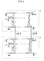
- FIG. 5 is a circuit diagram of a dual-phase cascode distributed amplifier according to a second preferred embodiment of the invention.
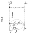
- FIG. 6 is a circuit diagram of a single-phase cascode distributed amplifier according to a third preferred embodiment of the invention.
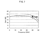
- FIG. 7 is a diagram for explaining the frequency characteristics of the distributed amplifier of the present embodiment in FIG. 6.
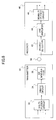
- FIG. 8 is a block diagram of an optical transmission system including the cascode distributed amplifier of the invention.
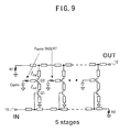
- FIG. 9 is a circuit diagram of a single-phase cascode distributed amplifier according to a fourth preferred embodiment of the invention.
- FIG. 10 is a diagram for explaining the frequency characteristics of the distributed amplifier of the present embodiment in FIG. 9.
- FIG. 11 is a circuit diagram of a single-phase cascode distributed amplifier according to a fifth preferred embodiment of the invention.
- FIG. 3 shows a single-phase cascode distributed amplifier according to a first preferred embodiment of the invention.
- the elements that are essentially the same as corresponding elements in FIG. 1 are designated by the same reference numerals.
- the cascode distributed amplifier of the present embodiment is constructed by the plurality of unit circuits (in the example of FIG. 3, seven unit circuits), each including the first transistor Q1 and the second transistor Q2, and the plurality of unit circuits are connected in parallel.
- An input signal IN is supplied to the input terminal 10 at one end of the input-side transmission wire, and an amplified signal OUT generated by the distributed amplifier is supplied from the output terminal 12 at one end of the output-side transmission wire.
- the resistor R1 is a termination resistor that is provided at the other end of the output-side transmission wire
- the resistor R2 is a termination resistor that is provided at the other end of the input-side transmission wire.
- Each of the rectangular blocks in FIG. 3 indicates an inductance component of a corresponding element of the transmission wires or the unit circuits.
- the sign " ⁇ " in FIG. 3 indicates that one end of the corresponding component such as a resistor, an inductor or a capacitor, is grounded.
- a damping resistor R gate is inserted between the grounding capacitor C gate and the inductance component l cg connected to the gate of the second transistor Q2 (called a grounded-gate transistor).
- FIG. 3 indicates that the damping resistor R gate is provided in the first-stage unit circuit only, the damping resistor R gate is provided in each of the seven unit circuits in the cascode distributed amplifier of the present embodiment of FIG. 3 in the same manner.
- the second transistor Q2 has a grounded gate which is grounded via the grounding capacitor C gate.
- the inductance component “l cg” which is connected at one end to the gate of the second transistor Q2, is connected at the other end to the damping resistor R gate .
- the damping resistor R gate which is connected at one end to the inductance component "l cg ", is connected at the other to the grounding capacitor C gate .
- the grounding capacitor C gate which is connected at one end to the damping resistor R gate , is grounded at the other end.
- the second transistor Q2 has a drain which is connected to the output-side transmission wire via an inductance component, and has a source which is connected to a drain of the first transistor Q1 via an inductance component "l sd ".
- the first transistor Q1 has a gate which is connected to the input-side transmission wire.
- the first transistor Q1 has a source which is grounded via an inductance component, and has a drain which is connected to the source of the second transistor Q2 via the inductance component "l sd ".
- the damping resistor R gate of each unit circuit acts to prevent the oscillation of the unit circuit.
- the damping resistor R gate of each unit circuit acts to change the Q value of the unit circuit in the decreasing direction.
- the damping resistor R gate functions to reduce the sensitivity of the unit circuit to frequencies in the high frequency range.
- the cascode distributed amplifier of the present embodiment is effective in preventing the rapid increase of the voltage gain (or the negative-polarity resistance) in the high frequency range as in the conventional cascode distributed amplifier, and it is possible to provide stable amplifying operation even when the frequency of the input signal is in the high frequency range.
- FIG. 4 shows the frequency characteristics of the distributed amplifier of the present embodiment in FIG. 3.
- the abscissas axis is the frequency axis (in GHz)
- the ordinates axis indicates changes of the gain coefficient
- the ordinates axis is the voltage gain axis (in dB).
- the characteristics curve of the cascode distributed amplifier of the present embodiment with the damping resistors R gate provided in the respective unit circuits is indicated by "B" in FIG. 4.
- the characteristics curve of the conventional cascode distributed amplifier in FIG. 1 without the damping resistor R gate is indicated by "A" in FIG. 4.
- the stability of the amplifying operation of the conventional cascode distributed amplifier deteriorates in the frequency range of 60 GHz or above.
- of the conventional amplifier has a rapid increase (abnormal peaking) in the frequency range of 60 GHz or above.
- the characteristic curve of the present embodiment shows that the voltage gain
- the cascode distributed amplifier of the present embodiment is effective in preventing the rapid increase of the negative-polarity resistance in the high frequency range as in the conventional cascode distributed amplifier, and it is possible to provide stable amplifying operation even when the frequency of the input signal is in the high frequency range.
- the cascode distributed amplifier of the present embodiment is effective in preventing the deterioration of the eye pattern at the receiving side, and it is possible to reduce the error ratio.
- the voltage gain of the cascode distributed amplifier of the present embodiment in the frequency range of 0 GHz to 60 GHz is gradually increased by about 2 dB.
- the cascode distributed amplifier of the present embodiment has a gain-raising characteristic, which compensates for variations of the frequency characteristics of the subsequently connected circuit or the LN modulator.
- the damping resistor R gate provided in each of the unit circuits of the cascode distributed amplifier of the present embodiment has a predetermined resistance value that is adequate for preventing the oscillation of each unit circuit in the high frequency range.
- the damping resistor R gate has such a resistance value that makes the reflection coefficient
- the amplifier circuit of the present embodiment in FIG. 3 is constructed on a single semiconductor chip.
- the damping resistor R gate is formed by an epitaxial resistor or a thin-film diffused resistor. It is difficult that the damping resistor R gate , formed on a normal transmission wire, has the necessary resistance value, and it is necessary to provide the damping resistor R gate connected to an end of the transmission wire.
- the grounding capacitor C gate is formed by an thin-film capacitor, a diffused capacitor or a metal-oxide semiconductor (MOS) transistor.
- MOS metal-oxide semiconductor
- the cascode distributed amplifier having the damping resistor R gate in each of the unit circuits prevents the rapid increase of the negative-polarity resistance in the high frequency range, and, by using the negative-polarity resistance, it provides stable amplifying operation even when the frequency of the input signal is in the high frequency range.
- FIG. 5 shows a dual-phase cascode distributed amplifier according to a second preferred embodiment of the invention.
- the elements that are essentially the same as corresponding elements in FIG. 3 are designated by the same reference numerals.
- the dual-phase cascode distributed amplifier of the present embodiment is constructed by two single-phase cascode distributed amplifiers 20 and 22 that are connected together via constant-current sources 18.
- the dual-phase cascode distributed amplifier of the present embodiment amplifies differential input signals IN+ and IN- received from input terminals 10 and 14, and supplies the amplified differential signals OUT+ and OUT- to output terminals 12 and 16.
- Each of the single-phase cascode distributed amplifiers 20 and 22 has the configuration that is the same as the configuration of the cascode distributed amplifier shown in FIG. 3. Namely, in each of the cascode distributed amplifiers 20 and 22, a plurality of unit circuits, each including the first transistor Q1 and the second transistor Q2, are connected in parallel. Similar to the previous embodiment of FIG. 3, the damping resistor R gate is provided in each of the unit circuits in each of the cascode distributed amplifiers 20 and 22 of the present embodiment in the same manner. In each unit circuit, the damping resistor R gate is inserted between the grounding capacitor C gate and the inductance component l cg connected to the gate of the second transistor Q2. Other elements in the present embodiment of FIG. 5 are essentially the same as the corresponding elements in the previous embodiment of FIG. 3, and a description thereof will be omitted.
- the single-phase cascode distributed amplifiers 20 and 22, and the constant-current sources 18 are constructed on a single semiconductor chip.
- the source of the first transistor Q1 of each of the unit circuits of the cascode distributed amplifier 20 and the source of the first transistor Q1 of each of the unit circuits of the cascode distributed amplifier 22 are connected together via the corresponding one of the constant-current sources 18.
- the electric current flowing into the source of the first transistor Q1 of each unit circuit is pulled into the corresponding one of the constant-current sources 18.
- the differential input signals IN+ and IN- are respectively supplied to the input terminals 10 and 14 of the amplifiers 20 and 22, and the amplified differential signals OUT+ and OUT-, generated by the amplifiers 20 and 22, are respectively supplied from the output terminals 12 and 16 to inputs of a subsequently connected circuit.
- each of the single-phase cascode distributed amplifiers 20 and 22 having the damping resistor R gate in each of the unit circuits prevents the rapid increase of the negative-polarity resistance in the high frequency range, and, by using the negative-polarity resistance, it provides stable amplifying operation even when the frequency of the input signal is in the high frequency range.
- FIG. 6 shows a single-phase cascode distributed amplifier according to a third preferred embodiment of the invention.
- the elements that are essentially the same as corresponding elements in FIG. 3 are designated by the same reference numerals.
- the grounding capacitor C gate has a fixed capacitance value.
- the grounding capacitor C gate of the present embodiment has a variable capacitance value.
- the grounding capacitor C gate of this type is constructed by using a varactor diode.
- Other elements in the present embodiment of FIG. 6 are essentially the same as the corresponding elements in the previous embodiment of FIG. 3, and a description thereof will be omitted.
- a variable capacitance value provided by the grounding capacitor C gate is used, and it is possible to change the value of the negative-polarity resistance.
- FIG. 7 shows the frequency characteristics of the distributed amplifier of the present embodiment in FIG. 6 when a control voltage applied to the grounding capacitor C gate is changed.
- the grounding capacitor C gate having a variable capacitance value is provided, and the grounding capacitor C gate is constructed by using a varactor diode.
- the control voltage applied to the grounding capacitor C gate the varactor diode
- the cascode distributed amplifier of the present embodiment shows, when the capacitance value provided by the grounding capacitor C gate remain unchanged, the initial frequency characteristics indicated by the lower characteristic curve in FIG. 7.
- the cascode distributed amplifier of the present embodiment shows the frequency characteristics indicated by the upper characteristic curve in FIG. 7.
- the cascode distributed amplifier of the present embodiment provides a gain-raising characteristic that amounts to 2 dB.
- the cascode distributed amplifier of the present embodiment is able to compensate for variations of the frequency characteristics of the subsequently connected circuit due to changes of the manufacturing conditions.
- the output of the LN modulator provides flat frequency characteristics, and it is possible to obtain a good eye pattern.
- the amplifier circuit of FIG. 6 When the amplifier circuit of FIG. 6 is formed on a semiconductor chip such that a control voltage is applied to the varactor diode, it is necessary that an external terminal to which the control voltage is supplied be provided on the chip. In such a case, the external terminal may be shared by the respective unit circuits of the amplifier.
- both the damping resistor R gate and the variable grounding capacitor C gate be provided in the cascode distributed amplifier.
- the damping resistor R gate is omitted from the amplifier circuit shown in FIG. 6, the cascode distributed amplifier in such alternative embodiment provides the gain-raising characteristic shown in FIG. 7.
- the cascode distributed amplifier having no damping resistor R gate does not prevent the rapid increase of the voltage gain in the high frequency band of about 50 GHz as shown in FIG. 2, and the frequency band that can be suitably used by the cascode distributed amplifier in such alternative embodiment is restricted.
- the grounding capacitor C gate having a variable capacitance value may be provided in the dual-phase cascode distributed amplifier of FIG. 5.
- both the single-phase cascode distributed amplifiers 20 and 22 provide the gain-raising characteristic shown in FIG. 7.
- the dual-phase cascode distributed amplifier in such alternative embodiment is able to compensate for variations of the frequency characteristics of a subsequently connected circuit (for example, an LN modulator) connected to the output terminals 12 and 16 of the amplifiers 20 and 22.
- the external terminals, needed for applying the control voltage to the varactor diode may be individually provided for the amplifiers 20 and 22. Alternatively, the external terminal which is shared by the amplifiers 20 and 22 may be provided.
- the damping resistor R gate may be omitted and only the variable grounding capacitor C gate may be provided.
- the dual-phase cascode distributed amplifier having no damping resistor R gate does not prevent the rapid increase of the voltage gain in the high frequency band of about 50 GHz as shown in FIG. 2, and the frequency band that can be suitably used by the cascode distributed amplifier in such alternative embodiment is restricted.
- FIG. 8 shows an optical transmission system in which the cascode distributed amplifier according to the present invention is provided.
- an optical transmitter 30 and an optical receiver 40 are connected together via an optical fiber cable 50.
- the transmitter 30 generally includes a multiplexer circuit 32, a driver circuit 34, and an LN (lithium niobate) modulator 36.
- a signal output by an internal circuit (not shown) is sent to the multiplexer circuit 32, and the multiplexer circuit 32 generates a multiplexed signal from the received signal.
- the driver circuit 34 In response to the multiplexed signal output by the multiplexer circuit 32, the driver circuit 34 generates a drive signal that is sent to the LN modulator 36. In response to the drive signal output by the driver circuit 34, the LN modulator 36 generates an optical modulated signal.
- the optical modulated signal output by the LN modulator is transmitted to the receiver 40 through the optical fiber cable 50.
- the cascode distributed amplifier of the present invention is incorporated in the driver circuit 34 of the transmitter 30.
- the receiver 40 generally includes a photodetector 42, a pre-amplifier 44, and a de-multiplexer circuit 46.
- the photodetector 42 receives the optical modulated signal from the optical fiber cable 50, and generates an electrical signal from the received optical signal.
- the pre-amplifier 44 provides amplification of the electrical signal output by the photodetector 42, and generates an amplified signal that is sent to the de-multiplexer circuit 46.
- the de-multiplexer circuit 46 In response to the amplified signal output by the pre-amplifier 44, the de-multiplexer circuit 46 generates a set of reconstructed signals from the received amplified signal. The reconstructed signals output by the de-multiplexer circuit 46 are sent to an internal circuit (not shown) of the receiver 40.
- the cascode distributed amplifier of the present invention is incorporated in the pre-amplifier 44 of the receiver 40.
- FIG. 9 shows a single-phase cascode distributed amplifier according to a fourth preferred embodiment of the invention.
- the elements that are essentially the same as corresponding elements in FIG. 3 are designated by the same reference numerals.
- the cascode distributed amplifier of the present embodiment is constructed by a plurality of unit circuits (in the example of FIG. 9, five unit circuits), each unit circuit including the first transistor Q1 and the second transistor Q2 connected in series between the input-side transmission wire and the output-side transmission wire, and the plurality of unit circuits are connected in parallel.
- An input signal IN is supplied to the input terminal 10 at one end of the input-side transmission wire, and an amplified signal OUT generated by the distributed amplifier is supplied from the output terminal 12 at one end of the output-side transmission wire.
- two of the five unit circuits which are located adjacent to the input terminal 10, include the damping resistor R gate that is provided between the grounding capacitor C gate and the inductance component l cg connected to the gate of the second transistor Q2.
- Other unit circuits than the above-mentioned two unit circuits do not include the damping resistor R gate .
- the damping resistors R gate of the two unit circuits act to prevent the oscillation of the corresponding unit circuit.
- the damping resistors R gate act to change the Q value of the corresponding unit circuit in the decreasing direction.
- the damping resistors R gate function to reduce the sensitivity of the unit circuit to frequencies in the high frequency range.
- the cascode distributed amplifier of the present embodiment is effective in preventing the rapid increase of the voltage gain (or the negative-polarity resistance) in the high frequency range as in the conventional cascode distributed amplifier, and it is possible to provide stable amplifying operation even when the frequency of the input signal is in the high frequency range.
- FIG. 10 shows the frequency characteristics of the distributed amplifier of the present embodiment in FIG. 9.
- the abscissas axis is the frequency axis (in GHz)
- the ordinates axis indicates changes of the voltage gain of the output signal to the input signal.
- the ordinates axis is the voltage gain axis (in dB).
- the characteristic curve of the cascode distributed amplifier of the present embodiment having the damping resistors R gate provided in the two unit circuits adjacent to the input terminal 10 is indicated by "B" in FIG. 10.
- the characteristics curve of the conventional cascode distributed amplifier in FIG. 1 having no damping resistor R gate is indicated by "A" in FIG. 10.
- the stability of the amplifying operation of the conventional amplifier deteriorates in the frequency range of 60 GHz or less.
- the voltage gain of the conventional amplifier has a rapid increase (abnormal peaking) in the frequency range of 60 GHz or less.
- the characteristic curve of the present embodiment shows a gradual decrease of the voltage gain in the frequency range of 60 GHz or less, and no rapid gain increase takes place.
- the cascode distributed amplifier of the present embodiment is effective in preventing the rapid increase of the negative-polarity resistance in the high frequency range as in the conventional amplifier, and it is possible to provide stable amplifying operation even when the frequency of the input signal is in the high frequency range.
- the damping resistors R gate are provided only in the two unit circuits which are located adjacent to the input terminal 10 in the cascode distributed amplifier.
- the damping resistors R gate may be provided in two or more unit circuits located adjacent to the input terminal 10. In such alternative embodiment, it is possible to strengthen the effects of providing stable amplifying operation.
- damping resistors R gate may be provided in the two unit circuits which are located adjacent to the output terminal 12 in the cascode distributed amplifier, which will be described below.
- FIG. 11 shows a single-phase cascode distributed amplifier according to a fifth preferred embodiment of the invention.
- the elements that are essentially the same as corresponding elements in FIG. 3 are designated by the same reference numerals.
- the cascode distributed amplifier of the present embodiment is constructed by a plurality of unit circuits (in the example of FIG. 11, five unit circuits), each unit circuit including the first transistor Q1 and the second transistor Q2 connected in series between the input-side transmission wire and the output-side transmission wire, and the plurality of unit circuits are connected in parallel.
- An input signal IN is supplied to the input terminal 10 at one end of the input-side transmission wire, and an amplified signal OUT generated by the distributed amplifier is supplied from the output terminal 12 at one end of the output-side transmission wire.
- two of the five unit circuits which are located adjacent to the output terminal 12, include the damping resistor R gate that is provided between the grounding capacitor C gate and the inductance component l cg connected to the gate of the second transistor Q2.
- Other unit circuits than the above-mentioned two unit circuits do not include the damping resistor R gate .
- the damping resistors R gate of the two unit circuits act to prevent the oscillation of the corresponding unit circuit.
- the damping resistors R gate act to change the Q value of the corresponding unit circuit in the decreasing direction.
- the damping resistors R gate function to reduce the sensitivity of the unit circuit to frequencies in the high frequency range.
- the cascode distributed amplifier of the present embodiment is effective in preventing the rapid increase of the voltage gain (or the negative-polarity resistance) in the high frequency range as in the conventional cascode distributed amplifier, and it is possible to provide stable amplifying operation even when the frequency of the input signal is in the high frequency range.
- a dual-phase cascode distributed amplifier can be constructed by connecting a first single-phase cascode distributed amplifier 20 and a second single-phase cascode distributed amplifier 22 which are configured according to the embodiment of FIG. 9 or the embodiment of FIG. 11.
- the two of the five unit circuits in the amplifier 20, located adjacent to the input terminal 10 and the two of the five unit circuits in the amplifier 22, located adjacent to the input terminal 14, include the damping resistors R gate that are provided between the grounding capacitor C gate and the inductance component l cg connected to the gate of the second transistor Q2.
- Other unit circuits than the above-mentioned unit circuits do not include the damping resistor R gate .
- the two of the five unit circuits in the amplifier 20, located adjacent to the output terminal 12, and the two of the five unit circuits in the amplifier 22, located adjacent to the output terminal 16, may include the damping resistors R gate .
- the cascode distributed amplifier employs field-effect transistors (FET) as the first and second transistors Q1 and Q2.
- FET field-effect transistors
- BJT bipolar junction transistors
- the five or seven unit circuits are connected in parallel within the single-phase cascode distributed amplifier.
- the present invention is not limited to these embodiments. It is readily understood that an arbitrary number of unit circuits may be provided within the single-phase cascode distributed amplifier without departing from the scope of the present invention.
- the cascode distributed amplifier of the invention may be configured such that the damping resistor R gate of each unit circuit has a variable resistance value.
- the appropriate value of the resistance provided by the damping resistor R gate may be determined through experimental computer simulations, for example.
- the use of the damping resistor R gate having a variable resistance value is not always needed.
- the demands of the users for the desired frequency characteristics of the amplifier may be satisfied by the use of the damping resistor R gate having a variable resistance value.
- a terminal used to adjust the variable resistance of the damping resistor R gate is provided on a chip, and, by changing a control voltage supplied to the terminal of the chip, the adjustment of the variable resistance of the damping resistor R gate to the desired value can be realized.
- the cascode distributed amplifier of the present invention is provided in an optical transmission system.
- the cascode distributed amplifier of the present invention may be provided in another transmission system.
Landscapes
- Engineering & Computer Science (AREA)
- Power Engineering (AREA)
- Microwave Amplifiers (AREA)
- Amplifiers (AREA)
Applications Claiming Priority (4)
| Application Number | Priority Date | Filing Date | Title |
|---|---|---|---|
| JP2001210672 | 2001-07-11 | ||
| JP2001210672 | 2001-07-11 | ||
| JP2002034069A JP4751002B2 (ja) | 2001-07-11 | 2002-02-12 | カスコード型分布増幅器 |
| JP2002034069 | 2002-02-12 |
Publications (3)
| Publication Number | Publication Date |
|---|---|
| EP1276230A2 true EP1276230A2 (de) | 2003-01-15 |
| EP1276230A3 EP1276230A3 (de) | 2003-05-28 |
| EP1276230B1 EP1276230B1 (de) | 2008-12-10 |
Family
ID=26618516
Family Applications (1)
| Application Number | Title | Priority Date | Filing Date |
|---|---|---|---|
| EP02251848A Expired - Lifetime EP1276230B1 (de) | 2001-07-11 | 2002-03-14 | Kaskodenkettenverstärker |
Country Status (5)
| Country | Link |
|---|---|
| US (1) | US6864750B2 (de) |
| EP (1) | EP1276230B1 (de) |
| JP (1) | JP4751002B2 (de) |
| CA (1) | CA2376410C (de) |
| DE (1) | DE60230216D1 (de) |
Cited By (3)
| Publication number | Priority date | Publication date | Assignee | Title |
|---|---|---|---|---|
| EP1633041A3 (de) * | 2004-09-07 | 2006-07-05 | Integrant Technologies Inc. | Aktive Schaltung mit verbesserter Linearität mittels Transistoren in Gateschaltung |
| CN103812455A (zh) * | 2012-11-09 | 2014-05-21 | 三菱电机株式会社 | 共阴共栅放大器 |
| EP2498399A3 (de) * | 2011-03-09 | 2015-11-11 | Hittite Microwave Corporation | Verteilter Verstärker mit verbesserter Stabilisierung |
Families Citing this family (36)
| Publication number | Priority date | Publication date | Assignee | Title |
|---|---|---|---|---|
| JP4659826B2 (ja) | 2004-06-23 | 2011-03-30 | ペレグリン セミコンダクター コーポレーション | Rfフロントエンド集積回路 |
| US6965722B1 (en) * | 2004-10-29 | 2005-11-15 | Finisar Corporation | High efficiency active matching electro-optic transducer driver circuit operable with low supply voltages |
| JP4821214B2 (ja) * | 2005-08-26 | 2011-11-24 | 三菱電機株式会社 | カスコード接続回路 |
| US7652539B2 (en) * | 2005-10-31 | 2010-01-26 | Huai Gao | Multi-stage broadband amplifiers |
| EP2166667B1 (de) * | 2006-03-20 | 2012-02-01 | Fujitsu Limited | Analoge Schaltung |
| US7489201B2 (en) * | 2006-05-10 | 2009-02-10 | Georgia Tech Research Corp. | Millimeter-wave cascode amplifier gain boosting technique |
| US20100226411A1 (en) * | 2006-09-20 | 2010-09-09 | Manabu Watanabe | Low-noise amplifier and radio communication system |
| US7843268B2 (en) * | 2008-04-17 | 2010-11-30 | Hittite Microwave Corporation | Modified distributed amplifier to improve low frequency efficiency and noise figure |
| JP5217728B2 (ja) * | 2008-07-24 | 2013-06-19 | 富士通株式会社 | 増幅器 |
| JP2010068261A (ja) * | 2008-09-11 | 2010-03-25 | Mitsubishi Electric Corp | カスコード回路 |
| JP4965602B2 (ja) * | 2009-05-19 | 2012-07-04 | 日本電信電話株式会社 | 差動分布回路icパッケージ |
| JP4951022B2 (ja) * | 2009-05-19 | 2012-06-13 | 日本電信電話株式会社 | 差動分布回路 |
| US8487706B2 (en) * | 2010-01-25 | 2013-07-16 | Peregrine Semiconductor Corporation | Stacked linear power amplifier with capacitor feedback and resistor isolation |
| US9859882B2 (en) | 2011-03-21 | 2018-01-02 | Infineon Technologies Americas Corp. | High voltage composite semiconductor device with protection for a low voltage device |
| US8766375B2 (en) | 2011-03-21 | 2014-07-01 | International Rectifier Corporation | Composite semiconductor device with active oscillation prevention |
| US20120241820A1 (en) * | 2011-03-21 | 2012-09-27 | International Rectifier Corporation | III-Nitride Transistor with Passive Oscillation Prevention |
| US9362905B2 (en) | 2011-03-21 | 2016-06-07 | Infineon Technologies Americas Corp. | Composite semiconductor device with turn-on prevention control |
| US8680928B2 (en) * | 2012-03-29 | 2014-03-25 | Avago Technologies General Ip (Singapore) Pte. Ltd. | Power amplifier including variable capacitor circuit |
| US9071289B2 (en) * | 2012-04-23 | 2015-06-30 | Cambridge Silicon Radio Limited | Transceiver supporting multiple modulation schemes |
| US9240756B1 (en) * | 2013-03-12 | 2016-01-19 | Lockheed Martin Corporation | High linearity, high efficiency, low noise, gain block using cascode network |
| JP6201391B2 (ja) | 2013-04-16 | 2017-09-27 | 三菱電機株式会社 | 電力増幅器 |
| JP6372030B2 (ja) * | 2013-04-16 | 2018-08-15 | 株式会社村田製作所 | 電力増幅器 |
| US9219450B1 (en) * | 2014-01-07 | 2015-12-22 | Lockheed Martin Corporation | High linearity low noise amplifier |
| US9679893B2 (en) * | 2015-05-15 | 2017-06-13 | Taiwan Semiconductor Manufacturing Company Limited | Semiconductor device and transistor |
| CN109075750A (zh) | 2016-02-04 | 2018-12-21 | 弗劳恩霍夫应用研究促进协会 | 矩阵功率放大器 |
| US9837965B1 (en) | 2016-09-16 | 2017-12-05 | Peregrine Semiconductor Corporation | Standby voltage condition for fast RF amplifier bias recovery |
| US9960737B1 (en) | 2017-03-06 | 2018-05-01 | Psemi Corporation | Stacked PA power control |
| US10715091B2 (en) * | 2017-10-13 | 2020-07-14 | Samsung Electronics Co., Ltd. | Low-noise amplifier supporting beam-forming function and receiver including the same |
| KR20190041896A (ko) | 2017-10-13 | 2019-04-23 | 삼성전자주식회사 | 빔포밍 기능을 지원하기 위한 저잡음 증폭기 및 이를 포함하는 수신기 |
| US11515850B2 (en) | 2018-09-04 | 2022-11-29 | Nippon Telegraph And Telephone Corporation | Distributed amplifier |
| JP2020096294A (ja) * | 2018-12-13 | 2020-06-18 | 株式会社村田製作所 | 電力増幅回路 |
| CN112212447B (zh) * | 2019-07-11 | 2024-12-06 | 北京莱恩创科纳米科技有限公司 | 一种增强型光催化抗菌除味全热交换新风机 |
| JP7480845B2 (ja) * | 2020-06-26 | 2024-05-10 | 日本電信電話株式会社 | 合波器 |
| CN112234945B (zh) * | 2020-10-14 | 2024-02-27 | 联合微电子中心有限责任公司 | 分布式放大器电路、增益单元和电子装置 |
| US20240243709A1 (en) * | 2023-01-13 | 2024-07-18 | Qorvo Us, Inc. | Methods and techniques to improve stability of cascode amplifiers and enhance lineup efficiency in multi-stage power amplifiers |
| CN119628576A (zh) * | 2025-02-17 | 2025-03-14 | 成都信息工程大学 | 一种高鲁棒性分布式放大器 |
Family Cites Families (8)
| Publication number | Priority date | Publication date | Assignee | Title |
|---|---|---|---|---|
| US2943267A (en) * | 1955-10-31 | 1960-06-28 | Sperry Rand Corp | Series-energized transistor amplifier |
| GB1098979A (en) * | 1965-07-03 | 1968-01-10 | Marconi Co Ltd | Improvements in or relating to high frequency transistor amplifiers |
| FR2558997B1 (fr) * | 1984-01-31 | 1989-02-03 | Thomson Csf | Amplificateur correcteur du temps de propagation de groupe de signaux electriques et chaine d'amplification a frequence intermediaire de faisceaux hertziens comportant un tel amplificateur |
| US5196805A (en) | 1992-01-31 | 1993-03-23 | Motorola, Inc. | Distributed differential amplifier arrangement |
| JP3056933B2 (ja) * | 1993-12-16 | 2000-06-26 | 日本電信電話株式会社 | 分布型バラン |
| US6137367A (en) * | 1998-03-24 | 2000-10-24 | Amcom Communications, Inc. | High power high impedance microwave devices for power applications |
| CN1187890C (zh) * | 1998-07-07 | 2005-02-02 | 松下电器产业株式会社 | 半导体放大器电路与系统 |
| JP4206589B2 (ja) * | 1999-12-02 | 2009-01-14 | 富士通株式会社 | 分布増幅器 |
-
2002
- 2002-02-12 JP JP2002034069A patent/JP4751002B2/ja not_active Expired - Lifetime
- 2002-03-14 EP EP02251848A patent/EP1276230B1/de not_active Expired - Lifetime
- 2002-03-14 US US10/096,865 patent/US6864750B2/en not_active Expired - Lifetime
- 2002-03-14 CA CA002376410A patent/CA2376410C/en not_active Expired - Lifetime
- 2002-03-14 DE DE60230216T patent/DE60230216D1/de not_active Expired - Lifetime
Cited By (8)
| Publication number | Priority date | Publication date | Assignee | Title |
|---|---|---|---|---|
| EP1633041A3 (de) * | 2004-09-07 | 2006-07-05 | Integrant Technologies Inc. | Aktive Schaltung mit verbesserter Linearität mittels Transistoren in Gateschaltung |
| CN100561862C (zh) * | 2004-09-07 | 2009-11-18 | 因特格瑞特科技有限公司 | 使用多个选通晶体管的具有改进线性的有源电路 |
| EP2498399A3 (de) * | 2011-03-09 | 2015-11-11 | Hittite Microwave Corporation | Verteilter Verstärker mit verbesserter Stabilisierung |
| US9425752B2 (en) | 2011-03-09 | 2016-08-23 | Hittite Microwave Llc | Distributed amplifier with improved stabilization |
| US10122325B2 (en) | 2011-03-09 | 2018-11-06 | Hittite Microwave Llc | Distributed amplifier with improved stabilization |
| US10164579B2 (en) | 2011-03-09 | 2018-12-25 | Hittite Microwave Llc | Distributed amplifier |
| CN103812455A (zh) * | 2012-11-09 | 2014-05-21 | 三菱电机株式会社 | 共阴共栅放大器 |
| CN103812455B (zh) * | 2012-11-09 | 2017-01-04 | 三菱电机株式会社 | 共阴共栅放大器 |
Also Published As
| Publication number | Publication date |
|---|---|
| JP4751002B2 (ja) | 2011-08-17 |
| CA2376410C (en) | 2004-11-09 |
| DE60230216D1 (de) | 2009-01-22 |
| EP1276230A3 (de) | 2003-05-28 |
| EP1276230B1 (de) | 2008-12-10 |
| US20030011436A1 (en) | 2003-01-16 |
| US6864750B2 (en) | 2005-03-08 |
| CA2376410A1 (en) | 2003-01-11 |
| JP2003092523A (ja) | 2003-03-28 |
Similar Documents
| Publication | Publication Date | Title |
|---|---|---|
| US6864750B2 (en) | Cascode distributed amplifier | |
| US6768380B2 (en) | Wideband, variable-bandwidth distributed amplifier | |
| US4998012A (en) | Fiber optic transimpedance receiver | |
| JP2008510383A5 (de) | ||
| US12362715B2 (en) | Voltage controlled attenuator | |
| US12113483B2 (en) | DC coupled amplifier having pre-driver and bias control | |
| US5862464A (en) | Pin diode variable attenuator | |
| US11329729B2 (en) | Optical receiver circuit, optical receiver, optical terminal device, and optical communication system | |
| JP5308243B2 (ja) | 可変ゲイン回路 | |
| US6930557B2 (en) | Multi-stage amplifier | |
| US6801098B2 (en) | Group delay equalizer integrated with a wideband distributed amplifier monolithic microwave integrated circuit | |
| US20060097777A1 (en) | Architecture for transverse-form analog finite-impulse-response filter | |
| JP3937426B2 (ja) | プリアンプ回路 | |
| US12021489B2 (en) | Amplifier circuit for driving electro-optical modulators with reduced process, voltage and temperature (PVT) sensitivity | |
| US6914488B2 (en) | Broadband amplification apparatus for bandwidth expansion | |
| US20250192732A1 (en) | Integrated circuit ac coupling design with adjusted-ratio and high impedance emitter follower stage | |
| JP7497316B2 (ja) | 周波数特性可変差動リニアアンプ | |
| EP0916183A1 (de) | Transimpedanzverstärker | |
| EP1001528A2 (de) | Integrierter Transimpedanzverstärker | |
| JPH11191740A (ja) | 信号調整器 |
Legal Events
| Date | Code | Title | Description |
|---|---|---|---|
| PUAI | Public reference made under article 153(3) epc to a published international application that has entered the european phase |
Free format text: ORIGINAL CODE: 0009012 |
|
| AK | Designated contracting states |
Kind code of ref document: A2 Designated state(s): AT BE CH CY DE DK ES FI FR GB GR IE IT LI LU MC NL PT SE TR |
|
| AX | Request for extension of the european patent |
Free format text: AL;LT;LV;MK;RO;SI |
|
| PUAL | Search report despatched |
Free format text: ORIGINAL CODE: 0009013 |
|
| AK | Designated contracting states |
Designated state(s): AT BE CH CY DE DK ES FI FR GB GR IE IT LI LU MC NL PT SE TR |
|
| AX | Request for extension of the european patent |
Extension state: AL LT LV MK RO SI |
|
| 17P | Request for examination filed |
Effective date: 20030714 |
|
| AKX | Designation fees paid |
Designated state(s): DE FR GB IT |
|
| 17Q | First examination report despatched |
Effective date: 20070102 |
|
| GRAP | Despatch of communication of intention to grant a patent |
Free format text: ORIGINAL CODE: EPIDOSNIGR1 |
|
| GRAS | Grant fee paid |
Free format text: ORIGINAL CODE: EPIDOSNIGR3 |
|
| GRAS | Grant fee paid |
Free format text: ORIGINAL CODE: EPIDOSNIGR3 |
|
| GRAA | (expected) grant |
Free format text: ORIGINAL CODE: 0009210 |
|
| RIN1 | Information on inventor provided before grant (corrected) |
Inventor name: SHIGEMATSU, HISAO |
|
| AK | Designated contracting states |
Kind code of ref document: B1 Designated state(s): DE FR GB IT |
|
| REG | Reference to a national code |
Ref country code: GB Ref legal event code: FG4D |
|
| REF | Corresponds to: |
Ref document number: 60230216 Country of ref document: DE Date of ref document: 20090122 Kind code of ref document: P |
|
| PLBE | No opposition filed within time limit |
Free format text: ORIGINAL CODE: 0009261 |
|
| STAA | Information on the status of an ep patent application or granted ep patent |
Free format text: STATUS: NO OPPOSITION FILED WITHIN TIME LIMIT |
|
| 26N | No opposition filed |
Effective date: 20090911 |
|
| REG | Reference to a national code |
Ref country code: FR Ref legal event code: PLFP Year of fee payment: 15 |
|
| REG | Reference to a national code |
Ref country code: FR Ref legal event code: PLFP Year of fee payment: 16 |
|
| REG | Reference to a national code |
Ref country code: FR Ref legal event code: PLFP Year of fee payment: 17 |
|
| PGFP | Annual fee paid to national office [announced via postgrant information from national office to epo] |
Ref country code: FR Payment date: 20210210 Year of fee payment: 20 |
|
| PGFP | Annual fee paid to national office [announced via postgrant information from national office to epo] |
Ref country code: DE Payment date: 20210302 Year of fee payment: 20 Ref country code: GB Payment date: 20210308 Year of fee payment: 20 |
|
| PGFP | Annual fee paid to national office [announced via postgrant information from national office to epo] |
Ref country code: IT Payment date: 20210211 Year of fee payment: 20 |
|
| REG | Reference to a national code |
Ref country code: DE Ref legal event code: R071 Ref document number: 60230216 Country of ref document: DE |
|
| REG | Reference to a national code |
Ref country code: GB Ref legal event code: PE20 Expiry date: 20220313 |
|
| PG25 | Lapsed in a contracting state [announced via postgrant information from national office to epo] |
Ref country code: GB Free format text: LAPSE BECAUSE OF EXPIRATION OF PROTECTION Effective date: 20220313 |