EP1276291A2 - Synchronistion de symbôles dans a récepteur multiporteuse - Google Patents
Synchronistion de symbôles dans a récepteur multiporteuse Download PDFInfo
- Publication number
- EP1276291A2 EP1276291A2 EP02254020A EP02254020A EP1276291A2 EP 1276291 A2 EP1276291 A2 EP 1276291A2 EP 02254020 A EP02254020 A EP 02254020A EP 02254020 A EP02254020 A EP 02254020A EP 1276291 A2 EP1276291 A2 EP 1276291A2
- Authority
- EP
- European Patent Office
- Prior art keywords
- adjustment
- time
- symbol
- impulse response
- synch
- Prior art date
- Legal status (The legal status is an assumption and is not a legal conclusion. Google has not performed a legal analysis and makes no representation as to the accuracy of the status listed.)
- Granted
Links
- 230000004044 response Effects 0.000 claims abstract description 66
- 238000000034 method Methods 0.000 claims description 19
- 238000012935 Averaging Methods 0.000 claims description 10
- 230000002123 temporal effect Effects 0.000 claims description 5
- 238000004590 computer program Methods 0.000 claims 4
- 230000009466 transformation Effects 0.000 claims 2
- 238000012790 confirmation Methods 0.000 claims 1
- 239000000969 carrier Substances 0.000 description 24
- 238000002592 echocardiography Methods 0.000 description 23
- 230000000694 effects Effects 0.000 description 23
- 230000003595 spectral effect Effects 0.000 description 19
- 238000010586 diagram Methods 0.000 description 18
- 238000011084 recovery Methods 0.000 description 16
- 238000012937 correction Methods 0.000 description 12
- 238000012360 testing method Methods 0.000 description 8
- 230000003044 adaptive effect Effects 0.000 description 7
- 230000003111 delayed effect Effects 0.000 description 7
- 230000008569 process Effects 0.000 description 6
- 230000000875 corresponding effect Effects 0.000 description 5
- 238000001514 detection method Methods 0.000 description 5
- 238000012545 processing Methods 0.000 description 5
- 238000013459 approach Methods 0.000 description 4
- 238000012805 post-processing Methods 0.000 description 4
- 230000005284 excitation Effects 0.000 description 3
- 230000006870 function Effects 0.000 description 3
- 230000006872 improvement Effects 0.000 description 3
- 238000005070 sampling Methods 0.000 description 3
- 238000012546 transfer Methods 0.000 description 3
- 230000015556 catabolic process Effects 0.000 description 2
- 230000008859 change Effects 0.000 description 2
- 238000006243 chemical reaction Methods 0.000 description 2
- 238000004891 communication Methods 0.000 description 2
- 238000006731 degradation reaction Methods 0.000 description 2
- ISLJZDYAPAUORR-UHFFFAOYSA-N ethyl n-[2-[(5-nitrothiophene-2-carbonyl)amino]thiophene-3-carbonyl]carbamate Chemical compound C1=CSC(NC(=O)C=2SC(=CC=2)[N+]([O-])=O)=C1C(=O)NC(=O)OCC ISLJZDYAPAUORR-UHFFFAOYSA-N 0.000 description 2
- 230000010354 integration Effects 0.000 description 2
- 238000007781 pre-processing Methods 0.000 description 2
- 230000009467 reduction Effects 0.000 description 2
- 230000001360 synchronised effect Effects 0.000 description 2
- 239000000654 additive Substances 0.000 description 1
- 230000000996 additive effect Effects 0.000 description 1
- 230000005540 biological transmission Effects 0.000 description 1
- 230000000295 complement effect Effects 0.000 description 1
- 239000012141 concentrate Substances 0.000 description 1
- 230000002596 correlated effect Effects 0.000 description 1
- 230000001419 dependent effect Effects 0.000 description 1
- 238000006073 displacement reaction Methods 0.000 description 1
- 230000008030 elimination Effects 0.000 description 1
- 238000003379 elimination reaction Methods 0.000 description 1
- 239000000284 extract Substances 0.000 description 1
- 238000005562 fading Methods 0.000 description 1
- 239000003550 marker Substances 0.000 description 1
- 238000012986 modification Methods 0.000 description 1
- 230000004048 modification Effects 0.000 description 1
- 230000008450 motivation Effects 0.000 description 1
- 230000010363 phase shift Effects 0.000 description 1
- 230000002250 progressing effect Effects 0.000 description 1
- 238000009877 rendering Methods 0.000 description 1
- 230000003362 replicative effect Effects 0.000 description 1
- 238000004088 simulation Methods 0.000 description 1
Images





Classifications
-
- H—ELECTRICITY
- H04—ELECTRIC COMMUNICATION TECHNIQUE
- H04L—TRANSMISSION OF DIGITAL INFORMATION, e.g. TELEGRAPHIC COMMUNICATION
- H04L27/00—Modulated-carrier systems
- H04L27/26—Systems using multi-frequency codes
- H04L27/2601—Multicarrier modulation systems
- H04L27/2647—Arrangements specific to the receiver only
- H04L27/2655—Synchronisation arrangements
- H04L27/2662—Symbol synchronisation
-
- H—ELECTRICITY
- H04—ELECTRIC COMMUNICATION TECHNIQUE
- H04L—TRANSMISSION OF DIGITAL INFORMATION, e.g. TELEGRAPHIC COMMUNICATION
- H04L27/00—Modulated-carrier systems
- H04L27/26—Systems using multi-frequency codes
- H04L27/2601—Multicarrier modulation systems
- H04L27/2647—Arrangements specific to the receiver only
- H04L27/2655—Synchronisation arrangements
- H04L27/2689—Link with other circuits, i.e. special connections between synchronisation arrangements and other circuits for achieving synchronisation
- H04L27/2695—Link with other circuits, i.e. special connections between synchronisation arrangements and other circuits for achieving synchronisation with channel estimation, e.g. determination of delay spread, derivative or peak tracking
Definitions
- Receivers embodying the present invention provide an improved estimate of the synch time by combining a pilot assisted tracker with a guard adapted filter processor.
- the pilot assisted tracker estimates the synch time from a channel impulse response estimate generated from pilot signal samples.
- an ambiguity exists in a relative time of arrival of signal paths of the channel impulse response with respect to the main signal path. As such, there is a disadvantage in using the pilot assisted channel impulse response alone.
- a COFDM symbol which is modulated in accordance with DVB standard is generated by modulating K narrow band carriers in parallel with the data to be communicated.
- the COFDM symbols are formed in the frequency domain and then converted in the time domain using an Inverse Fourier Transform.
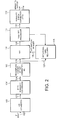
- Figure 1 A diagram representing the form of the COFDM symbols is shown in Figure 1.
- the re-sampling and carrier offset correction processor 106 is arranged to track in the frequency domain the K carriers of the COFDM modulation.
- the base band received signal samples are then fed to a Fast Fourier transform processor 108 which serves to convert the time domain received signal samples into the frequency domain.
- the data is then recovered from the frequency domain signal samples by a post FFT processor 110.
- the data is then fed to a forward error correction processor 112 which operates to decode the error correction encoded data to finally produce the recovered data at an output 114.
- Each OFDM transmitted symbol includes pilot sub-carriers centred at known frequencies which can be extracted from the output of the FFT and used to estimate the transfer function H(z) of the channel.
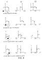
- the estimated channel transfer function H(z) can be inverse transformed via an IFFT to give a representation of the time domain channel impulse response (CIR). Symbol time tracking carried out on the CIR derived from such feedback can correct any symbol time acquisition errors that arose during initial symbol acquisition.
- CIR channel impulse response
- a guard adapted matched filter processor disclosed in [1] can be used to track an optimum SST.
- the noise floor should be low enough not to swamp any low power echoes that might be present.
- any adjustments needed to the CSST are determined in further processing as explained in [1]. In practice, this adjustment is very little in post-cursive channels, unless false spectral folding is detected in which case the channel is treated as pre-cursive.
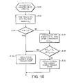
- the buffer that holds the samples for FFT processing is only N u locations long. This means that excessive adjustments to the SST might either result in loss of symbol samples through buffer overflow (for excessive negative adjustments) or buffer underflow (for excessive positive adjustments). Accordingly, there's a threshold of maximum adjustment ( D max ) during one OFDM symbol against which all adjustments must be tested. For any adjustment D > D max , only D max samples of adjustment to the SST are allowed. The residue ( D - D max ) must be held and applied during the next tracking period. Since the guard adapted matched filter processor cannot accurately operate with only a partially adjusted SST, PAT is invoked for this task.
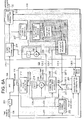
- FIG. 7 provides a block diagram of the PAT Output Processor 210 in more detail.
- the PAT Output Processor is comprised of the following processing blocks:
- the symbol time tracker runs the PAT asking it to provide only the TOA of the main path.
- the main path TOA goes to the guard adapted matched filter processor 204 where it is used to set up the taps and excitation of the matched filter for the next symbol tracking period.
- the main path TOA also goes to channel 207.3 of the switch 208 from where it proceeds to the symbol time adjustment estimator 206.
- This block uses the switch output to find the adjustment that needs to be made to the symbol sample counter or NCO 214. When the value in this counter reaches a preset value, the FFT Trigger Pulse Generator 212 generates a start pulse for the FFT block 108.
- the pre-processed output from the centre clip processor is then fed to a channel impulse response windowing processor 348.
- the windowing processor 348 provides a further pre-processing operation to the effect of isolating an analysis window within which the pre-processed output of the adaptive filter produces the maximum energy. It is within this analysis window that a peak output of the adaptive matched filter is determined by an error detection processor 350 with respect to the current time base derived from the current value of the NCO 214 through a feedback channel 213.
- the operation of the guard adapted matched filter processor 204 is controlled by a controller 360.
- the error detector 350 produces an adjustment to the CSST which is fed to channel 207.2 of switch 208 and selected as appropriate by the symbol timing adjustment estimator 206.
- the pre-processing operations performed by each of these processors are explained in more detail in [1].
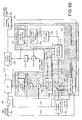
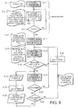
- the switch 208 is configured to receive a signal from the coarse symbol acquisition processor 202 as represented at step S2 in Figure 9. Before and during coarse symbol acquisition, the switch contact is set to channel 207.1. After acquisition it moves to channel 207.3 in readiness for the first symbol time tracking period.
- the coarse symbol acquisition processor 202 is operable to generate a signal representative of the TOA of the main path of the channel impulse response which is received by the symbol time adjustment estimator 206.
- the symbol time adjustment estimator 206 operates in combination with the NCO 214 and the FFT trigger pulse generator 212 to generate a first estimate of the SST provided to the FFT processor 108.
- slope correction is performed as well as channel estimation using by the pilot assisted channel estimator 252.
- frequency errors are calculated. This forms part of an initialization phase which also includes a step of carrier frequency recovery formed by process step S6 in combination with the decision step S8 which operate in a feedback loop to determine whether carrier frequency has been correctly recovered.
- the PAT output processor 210 operates to determine the TOA of the main path from the pilot assisted CIR estimate at step S12. At this point the switch 208 is arranged to connect the channel 207.3 from the PAT output processor 210 to the input of the symbol time adjustment estimator 206.
- the guard signal samples can be identified and the matched filter of the guard adapted matched filter processor 204 can be adapted so that the taps correspond accurately to the samples from the guard period. This is effected at step S14.
- the symbol timing adjustment estimator 206 sets the switch 208 to receive the adjustment from the guard adapted matched filter processor 204.
- the symbol timing adjustment estimator 206 then operates to adjust the symbol timing in accordance with the adjustment produced when the guard adapted matched filter processor 204 has gone through its integration period and its output processed to determine any adjustments to the CSST.
- pilot should be interpreted broadly as meaning any signal or data symbols which are transmitted with the data to be communicated and which are known to the received.
Landscapes
- Engineering & Computer Science (AREA)
- Computer Networks & Wireless Communication (AREA)
- Signal Processing (AREA)
- Noise Elimination (AREA)
- Synchronisation In Digital Transmission Systems (AREA)
- Structure Of Receivers (AREA)
- Transplanting Machines (AREA)
- Mobile Radio Communication Systems (AREA)
- Radio Transmission System (AREA)
- Cable Transmission Systems, Equalization Of Radio And Reduction Of Echo (AREA)
Applications Claiming Priority (2)
| Application Number | Priority Date | Filing Date | Title |
|---|---|---|---|
| GB0115061 | 2001-06-20 | ||
| GB0115061A GB2376855A (en) | 2001-06-20 | 2001-06-20 | Determining symbol synchronisation in an OFDM receiver in response to one of two impulse response estimates |
Publications (3)
| Publication Number | Publication Date |
|---|---|
| EP1276291A2 true EP1276291A2 (fr) | 2003-01-15 |
| EP1276291A3 EP1276291A3 (fr) | 2006-05-31 |
| EP1276291B1 EP1276291B1 (fr) | 2009-08-12 |
Family
ID=9916991
Family Applications (1)
| Application Number | Title | Priority Date | Filing Date |
|---|---|---|---|
| EP02254020A Expired - Lifetime EP1276291B1 (fr) | 2001-06-20 | 2002-06-10 | Synchronisation de symboles dans un récepteur multiporteuses |
Country Status (5)
| Country | Link |
|---|---|
| US (1) | US7177376B2 (fr) |
| EP (1) | EP1276291B1 (fr) |
| AT (1) | ATE439724T1 (fr) |
| DE (1) | DE60233297D1 (fr) |
| GB (1) | GB2376855A (fr) |
Cited By (1)
| Publication number | Priority date | Publication date | Assignee | Title |
|---|---|---|---|---|
| GB2382963A (en) * | 2001-11-13 | 2003-06-11 | Nec Corp | Adaptive optimal guard interval length determination in an OFDM receiver |
Families Citing this family (71)
| Publication number | Priority date | Publication date | Assignee | Title |
|---|---|---|---|---|
| US7020226B1 (en) * | 2002-04-04 | 2006-03-28 | Nortel Networks Limited | I/Q distortion compensation for the reception of OFDM signals |
| GB2388499A (en) | 2002-05-09 | 2003-11-12 | Sony Uk Ltd | A multi-carrier receiver which can detect, estimate and cancel impulse burst noise signals |
| US7369485B2 (en) * | 2002-08-19 | 2008-05-06 | Conexant, Inc. | Wireless receiver for sorting packets |
| AU2003268227A1 (en) * | 2002-08-28 | 2004-03-19 | Zyray Wireless, Inc. | Iterative multi-stage detection technique for a diversity receiver having multiple antenna elements |
| GB2395094A (en) * | 2002-10-28 | 2004-05-12 | Sony Uk Ltd | Determining a symbol synch time in an OFDM receiver |
| US20040223449A1 (en) * | 2003-05-08 | 2004-11-11 | Yih-Ming Tsuie | Mode detection for OFDM signals |
| AU2003238128A1 (en) * | 2003-06-30 | 2005-01-13 | Nokia Corporation | Faster fine timing operation in multi-carrier system |
| KR100606105B1 (ko) * | 2003-07-04 | 2006-07-28 | 삼성전자주식회사 | 다중 접속 방식을 사용하는 이동 통신 시스템의 셀 탐색장치 및 방법 |
| US8149961B1 (en) * | 2003-08-04 | 2012-04-03 | Regents Of The University Of Minnesota | Ranging in multi-band communication systems |
| JP4356392B2 (ja) | 2003-08-07 | 2009-11-04 | パナソニック株式会社 | 通信装置 |
| US7869488B2 (en) * | 2003-08-28 | 2011-01-11 | Qualcomm Incorporated | Method and apparatus for removing code aliases when using short synchronization codes |
| US20050047491A1 (en) * | 2003-08-28 | 2005-03-03 | Haitao Zhang | Method and apparatus for improving channel estimate based on short synchronization code |
| DE10342040A1 (de) * | 2003-09-11 | 2005-04-07 | Rohde & Schwarz Gmbh & Co Kg | Verfahren zur Überwachung der Zeitsynchronität von Sendern in einem Gleichwellennetz |
| AU2003267470A1 (en) * | 2003-10-03 | 2005-04-21 | Nokia Corporation | Method, system and receiver for receiving a multi-carrier transmission |
| EP1533968B1 (fr) * | 2003-11-11 | 2010-08-25 | NTT DoCoMo, Inc. | Dispositif de réception d'un signal et procédé de détection temporelle de réception |
| EP1531591A1 (fr) * | 2003-11-11 | 2005-05-18 | STMicroelectronics Belgium N.V. | Sélection d'échantillons pour une interpolation de domaine temporel |
| FR2868640B1 (fr) * | 2004-03-31 | 2006-06-09 | St Microelectronics Sa | Demodulateur cofdm a positionnement optimal de fenetre d'analyse fft |
| US7492828B2 (en) * | 2004-06-18 | 2009-02-17 | Qualcomm Incorporated | Time synchronization using spectral estimation in a communication system |
| US7585326B2 (en) | 2004-08-06 | 2009-09-08 | Spinalmotion, Inc. | Methods and apparatus for intervertebral disc prosthesis insertion |
| US20060045192A1 (en) * | 2004-08-25 | 2006-03-02 | Hiroshi Hayashi | Method and apparatus for pilot channel transmission and reception within a multi-carrier communication system |
| GB0419946D0 (en) * | 2004-09-08 | 2004-10-13 | British Telecomm | High data rate demodulation system |
| US20060088112A1 (en) * | 2004-09-08 | 2006-04-27 | Das Suvra S | Process and a system for transmission of data |
| GB0419947D0 (en) * | 2004-09-08 | 2004-10-13 | British Telecomm | High data rate demodulation system |
| DE102004047600A1 (de) * | 2004-09-30 | 2006-04-13 | Robert Bosch Gmbh | Verfahren zum Synchronisieren eines Abtasttaktes sowie Synchronisationseinheit für ein Mehrträgerempfangssystem |
| JP4167646B2 (ja) * | 2004-11-30 | 2008-10-15 | 株式会社東芝 | Ofdm復調装置 |
| JP4982186B2 (ja) * | 2004-12-21 | 2012-07-25 | パナソニック株式会社 | Ofdm受信装置 |
| US7778336B1 (en) * | 2005-02-09 | 2010-08-17 | Marvell International Ltd. | Timing and frequency synchronization of OFDM signals for changing channel conditions |
| US8675631B2 (en) * | 2005-03-10 | 2014-03-18 | Qualcomm Incorporated | Method and system for achieving faster device operation by logical separation of control information |
| US8144824B2 (en) * | 2005-03-10 | 2012-03-27 | Qualcomm Incorporated | Trend influenced time tracking |
| US20100157833A1 (en) * | 2005-03-10 | 2010-06-24 | Qualcomm Incorporated | Methods and systems for improved timing acquisition for varying channel conditions |
| US8315191B2 (en) * | 2005-09-20 | 2012-11-20 | Qualcomm Incorporated | Timing acquisition and mode and guard detection for an OFDM transmission |
| US7623607B2 (en) * | 2005-10-31 | 2009-11-24 | Qualcomm Incorporated | Methods and apparatus for determining timing in a wireless communication system |
| US8948329B2 (en) * | 2005-12-15 | 2015-02-03 | Qualcomm Incorporated | Apparatus and methods for timing recovery in a wireless transceiver |
| US8144818B2 (en) * | 2005-12-15 | 2012-03-27 | Qualcomm Incorporated | Apparatus and methods for determining timing in a communication system |
| KR101223783B1 (ko) * | 2006-03-06 | 2013-01-17 | 삼성전자주식회사 | 무선 통신 시스템에서 심벌 타이밍 오프셋 추정 장치 및방법 |
| JP4664234B2 (ja) * | 2006-05-24 | 2011-04-06 | 富士通セミコンダクター株式会社 | Ofdm受信機 |
| US7580468B2 (en) * | 2006-07-28 | 2009-08-25 | Samsung Electronics Co., Ltd. | Synchronization circuits, orthogonal frequency division multiplexing (OFDM) receivers, and related methods and computer program products |
| US8014457B2 (en) * | 2006-10-31 | 2011-09-06 | Freescale Semiconductor, Inc. | Method of providing a data signal for channel estimation and circuit thereof |
| US7684504B2 (en) * | 2006-10-31 | 2010-03-23 | Freescale Semiconductor, Inc. | System and method for reducing edge effect |
| WO2008056901A1 (fr) * | 2006-11-10 | 2008-05-15 | Electronics And Telecommunications Research Institute | Émetteurs pour étendre l'intervalle de protection d'un équipement utilisateurs individuel dans des systèmes d'accès mrof |
| KR100884556B1 (ko) * | 2006-11-10 | 2009-02-19 | 한국전자통신연구원 | 단일 반송파 주파수 분할 다중 접속 시스템에서 개별 사용자 단말의 보호구간 확장을 위한 송신장치 및 방법 |
| JP4312227B2 (ja) * | 2006-11-21 | 2009-08-12 | 富士通株式会社 | エコー処理方法及び装置 |
| US9391813B2 (en) * | 2007-02-16 | 2016-07-12 | Maxlinear, Inc. | Long echo detection and channel estimation for OFDM systems |
| US20080232482A1 (en) * | 2007-03-19 | 2008-09-25 | Legend Silicon Corp. | Method and apparatus for constructing receiver diversity for ofdm signals |
| US8416844B2 (en) | 2007-03-27 | 2013-04-09 | Panasonic Corporation | OFDM receiving apparatus, OFDM receiving method, OFDM receiving circuit, integrated circuit, and program |
| JP5108407B2 (ja) * | 2007-07-25 | 2012-12-26 | 富士通セミコンダクター株式会社 | シンボルタイミングリカバリ回路 |
| JP5098553B2 (ja) * | 2007-10-10 | 2012-12-12 | 富士通セミコンダクター株式会社 | Ofdm受信装置およびofdm受信方法 |
| JP2009111749A (ja) * | 2007-10-30 | 2009-05-21 | Sony Corp | 受信装置、受信方法、およびプログラム |
| JP4412387B2 (ja) * | 2007-10-30 | 2010-02-10 | ソニー株式会社 | 受信装置、受信方法、およびプログラム |
| TWI361588B (en) * | 2007-12-11 | 2012-04-01 | Ind Tech Res Inst | Method and device for detecting a synchronization signal in a communication system |
| US8750091B2 (en) * | 2008-03-31 | 2014-06-10 | Qualcomm Incorporated | Apparatus and methods for update of symbol information |
| CN101252764B (zh) * | 2008-04-03 | 2011-01-19 | 威盛电子股份有限公司 | 无线终端速度估计的方法及装置 |
| US8073064B2 (en) * | 2008-04-18 | 2011-12-06 | Newport Media, Inc. | Robust FFT trigger point tracking for echo channels in OFDM based communication systems |
| JP2009290725A (ja) * | 2008-05-30 | 2009-12-10 | Fujitsu Ltd | 受信装置および受信方法 |
| JP2011527061A (ja) * | 2008-07-07 | 2011-10-20 | ヒューレット−パッカード デベロップメント カンパニー エル.ピー. | データ・セキュリティのためのシステムおよび方法 |
| US8174958B2 (en) * | 2008-08-01 | 2012-05-08 | Broadcom Corporation | Method and system for a reference signal (RS) timing loop for OFDM symbol synchronization and tracking |
| JP4655241B2 (ja) * | 2008-09-30 | 2011-03-23 | ソニー株式会社 | 受信装置、受信方法、およびプログラム |
| US8396144B2 (en) * | 2008-12-31 | 2013-03-12 | Intel Corporation | Method and system for OFDM symbol timing recovery |
| CN101771650B (zh) * | 2009-01-07 | 2013-08-21 | 北京泰美世纪科技有限公司 | 一种ofdm系统的信道估计装置和方法 |
| BRPI1011213A2 (pt) * | 2009-05-29 | 2016-03-15 | Thomson Licensing | detecção e correção rápidas de salto de ciclo |
| GB2470768A (en) * | 2009-06-03 | 2010-12-08 | Sony Corp | Receiver for OFDM symbols in a MISO system with Alamouti-type encoding |
| US8280330B2 (en) * | 2009-12-30 | 2012-10-02 | Quintic Holdings | Crystal-less clock generation for radio frequency receivers |
| KR20130006935A (ko) * | 2011-06-27 | 2013-01-18 | 삼성전자주식회사 | 수신기 및 이의 동작 방법 |
| US9191240B2 (en) | 2011-10-04 | 2015-11-17 | St-Ericsson Sa | Processing of channel coefficients of a network |
| US8665973B2 (en) * | 2012-01-31 | 2014-03-04 | Exelis Inc. | Removal of a band-limited distributed pilot from an OFDM signal |
| US9160599B2 (en) * | 2013-08-12 | 2015-10-13 | Samsung Electronics Co., Ltd | Method and apparatus for channel smoothing and estimation in OFDM system |
| US10128917B2 (en) * | 2014-09-16 | 2018-11-13 | Qualcomm Incorporated | Systems and methods for tone plans for wireless communication networks |
| GB2525459B (en) * | 2014-10-22 | 2017-01-11 | Imagination Tech Ltd | Symbol boundary detection |
| US10834458B2 (en) | 2019-03-29 | 2020-11-10 | International Business Machines Corporation | Automated video detection and correction |
| US12334966B2 (en) * | 2022-08-01 | 2025-06-17 | Hughes Network Systems, Llc | Robust satellite beacon receiver |
| US12512917B2 (en) * | 2023-09-28 | 2025-12-30 | Mediatek Inc. | Digital signal processing system and method thereof |
Citations (2)
| Publication number | Priority date | Publication date | Assignee | Title |
|---|---|---|---|---|
| GB2369015A (en) | 2000-11-09 | 2002-05-15 | Sony Uk Ltd | Receiver that uses guard signals to estimate synchronisation position |
| GB2369016A (en) | 2000-11-09 | 2002-05-15 | Sony Uk Ltd | Receiver that detects a synchronisation position by representing samples as either positive or negative constants |
Family Cites Families (5)
| Publication number | Priority date | Publication date | Assignee | Title |
|---|---|---|---|---|
| FI108975B (fi) * | 1993-03-09 | 2002-04-30 | Nokia Corp | Opetusjakso digitaalisessa solukkopuhelinjärjestelmässä |
| FR2743967B1 (fr) * | 1996-01-18 | 1998-03-27 | France Telecom | Procede et dispositif de synchronisation temporelle d'un recepteur d'un signal multiporteuse |
| US6618452B1 (en) * | 1998-06-08 | 2003-09-09 | Telefonaktiebolaget Lm Ericsson (Publ) | Burst carrier frequency synchronization and iterative frequency-domain frame synchronization for OFDM |
| US6614864B1 (en) * | 1999-10-12 | 2003-09-02 | Itran Communications Ltd. | Apparatus for and method of adaptive synchronization in a spread spectrum communications receiver |
| US7106709B2 (en) * | 2000-11-29 | 2006-09-12 | Telefonaktiebologet Lm Ericsson (Publ) | Timing drift compensation in wireless packet-based systems |
-
2001
- 2001-06-20 GB GB0115061A patent/GB2376855A/en not_active Withdrawn
-
2002
- 2002-06-10 DE DE60233297T patent/DE60233297D1/de not_active Expired - Lifetime
- 2002-06-10 AT AT02254020T patent/ATE439724T1/de not_active IP Right Cessation
- 2002-06-10 EP EP02254020A patent/EP1276291B1/fr not_active Expired - Lifetime
- 2002-06-18 US US10/175,368 patent/US7177376B2/en not_active Expired - Lifetime
Patent Citations (2)
| Publication number | Priority date | Publication date | Assignee | Title |
|---|---|---|---|---|
| GB2369015A (en) | 2000-11-09 | 2002-05-15 | Sony Uk Ltd | Receiver that uses guard signals to estimate synchronisation position |
| GB2369016A (en) | 2000-11-09 | 2002-05-15 | Sony Uk Ltd | Receiver that detects a synchronisation position by representing samples as either positive or negative constants |
Non-Patent Citations (2)
| Title |
|---|
| "Timing Recovery for OFDM Transmission", IEEE JOURNAL ON SELECTED AREAS IN COMMUNICATIONS, vol. 18, no. 11, November 2000 (2000-11-01) |
| DONGHOON LEE ET AL.: "A New Symbol Timing Recovery Algorithm for OFDM Systems", IEEE TRANSACTIONS ON CONSUMER ELECTRONICS, vol. 10/43, no. 3, August 1997 (1997-08-01) |
Cited By (3)
| Publication number | Priority date | Publication date | Assignee | Title |
|---|---|---|---|---|
| GB2382963A (en) * | 2001-11-13 | 2003-06-11 | Nec Corp | Adaptive optimal guard interval length determination in an OFDM receiver |
| GB2382963B (en) * | 2001-11-13 | 2004-03-10 | Nec Corp | Guard interval length control method in OFDM, and related OFDM system, transmitting and receiving apparatuses |
| US7336598B2 (en) | 2001-11-13 | 2008-02-26 | Nec Corporation | Guard interval length control method in OFDM system and OFDM transmitting and receiving apparatuses |
Also Published As
| Publication number | Publication date |
|---|---|
| GB2376855A (en) | 2002-12-24 |
| US20030016773A1 (en) | 2003-01-23 |
| DE60233297D1 (de) | 2009-09-24 |
| EP1276291A3 (fr) | 2006-05-31 |
| US7177376B2 (en) | 2007-02-13 |
| ATE439724T1 (de) | 2009-08-15 |
| EP1276291B1 (fr) | 2009-08-12 |
| GB0115061D0 (en) | 2001-08-15 |
Similar Documents
| Publication | Publication Date | Title |
|---|---|---|
| EP1276291B1 (fr) | Synchronisation de symboles dans un récepteur multiporteuses | |
| EP1206096B1 (fr) | Synchronisation de l'horloge de symboles dans un récepteur multiporteuse | |
| US7027540B2 (en) | Receiver | |
| EP1624602B1 (fr) | Dispositif de demodulation et procede de demodulation | |
| EP0896457B1 (fr) | Synchronisation de symbole pour signaux multiporteurs à intervalle de garde | |
| US7388922B2 (en) | Receiver | |
| EP1416693A2 (fr) | Récupération de l'horloge de symboles dans un récepteur multiporteur | |
| US9391813B2 (en) | Long echo detection and channel estimation for OFDM systems | |
| EP1580951A2 (fr) | Récepteur | |
| EP1746794B1 (fr) | Sélection de trajet dans un dispositif OFDM | |
| US7668076B2 (en) | Multi-user receiving apparatus converting SC-FDMA received signals of all users to signals in a frequency domain commonly | |
| US20040141570A1 (en) | Symbol timing correction circuit, receiver, symbol timing correction, mothed, and demodulation processing method | |
| CN101507219A (zh) | 数据符号的时间误差估计 | |
| US7616723B2 (en) | Method for symbol timing synchronization and apparatus thereof | |
| WO2006018035A1 (fr) | Appareil et procede de reduction de derive de phase | |
| EP1755300B1 (fr) | Synchronisation dans des récepteurs multiporteuses | |
| JP4149302B2 (ja) | 伝送路特性推定装置、ofdm信号復調装置及び回り込みキャンセラ | |
| US20060018391A1 (en) | Method and apparatus of detecting isi/icsi in an ofdm system | |
| US20060018390A1 (en) | Method and apparatus of detecting isi/icsi in an ofdm system | |
| WO2008047277A2 (fr) | Détermination d'informations de synchronisation de symboles pour des signaux de multiplexage ofdm | |
| GB2419263A (en) | OFDM receiver coarse FFT window synch using centre of mass of correlation function and fine synch using weighted channel impulse response |
Legal Events
| Date | Code | Title | Description |
|---|---|---|---|
| PUAI | Public reference made under article 153(3) epc to a published international application that has entered the european phase |
Free format text: ORIGINAL CODE: 0009012 |
|
| AK | Designated contracting states |
Kind code of ref document: A2 Designated state(s): AT BE CH CY DE DK ES FI FR GB GR IE IT LI LU MC NL PT SE TR |
|
| AX | Request for extension of the european patent |
Free format text: AL;LT;LV;MK;RO;SI |
|
| PUAL | Search report despatched |
Free format text: ORIGINAL CODE: 0009013 |
|
| AK | Designated contracting states |
Kind code of ref document: A3 Designated state(s): AT BE CH CY DE DK ES FI FR GB GR IE IT LI LU MC NL PT SE TR |
|
| AX | Request for extension of the european patent |
Extension state: AL LT LV MK RO SI |
|
| 17P | Request for examination filed |
Effective date: 20060725 |
|
| AKX | Designation fees paid |
Designated state(s): AT BE CH CY DE DK ES FI FR GB GR IE IT LI LU MC NL PT SE TR |
|
| 17Q | First examination report despatched |
Effective date: 20070115 |
|
| GRAP | Despatch of communication of intention to grant a patent |
Free format text: ORIGINAL CODE: EPIDOSNIGR1 |
|
| GRAS | Grant fee paid |
Free format text: ORIGINAL CODE: EPIDOSNIGR3 |
|
| GRAA | (expected) grant |
Free format text: ORIGINAL CODE: 0009210 |
|
| AK | Designated contracting states |
Kind code of ref document: B1 Designated state(s): AT BE CH CY DE DK ES FI FR GB GR IE IT LI LU MC NL PT SE TR |
|
| REG | Reference to a national code |
Ref country code: GB Ref legal event code: FG4D |
|
| REG | Reference to a national code |
Ref country code: CH Ref legal event code: EP |
|
| REG | Reference to a national code |
Ref country code: IE Ref legal event code: FG4D |
|
| REF | Corresponds to: |
Ref document number: 60233297 Country of ref document: DE Date of ref document: 20090924 Kind code of ref document: P |
|
| PG25 | Lapsed in a contracting state [announced via postgrant information from national office to epo] |
Ref country code: ES Free format text: LAPSE BECAUSE OF FAILURE TO SUBMIT A TRANSLATION OF THE DESCRIPTION OR TO PAY THE FEE WITHIN THE PRESCRIBED TIME-LIMIT Effective date: 20091123 Ref country code: SE Free format text: LAPSE BECAUSE OF FAILURE TO SUBMIT A TRANSLATION OF THE DESCRIPTION OR TO PAY THE FEE WITHIN THE PRESCRIBED TIME-LIMIT Effective date: 20090812 Ref country code: FI Free format text: LAPSE BECAUSE OF FAILURE TO SUBMIT A TRANSLATION OF THE DESCRIPTION OR TO PAY THE FEE WITHIN THE PRESCRIBED TIME-LIMIT Effective date: 20090812 Ref country code: AT Free format text: LAPSE BECAUSE OF FAILURE TO SUBMIT A TRANSLATION OF THE DESCRIPTION OR TO PAY THE FEE WITHIN THE PRESCRIBED TIME-LIMIT Effective date: 20090812 |
|
| NLV1 | Nl: lapsed or annulled due to failure to fulfill the requirements of art. 29p and 29m of the patents act | ||
| PG25 | Lapsed in a contracting state [announced via postgrant information from national office to epo] |
Ref country code: NL Free format text: LAPSE BECAUSE OF FAILURE TO SUBMIT A TRANSLATION OF THE DESCRIPTION OR TO PAY THE FEE WITHIN THE PRESCRIBED TIME-LIMIT Effective date: 20090812 |
|
| PG25 | Lapsed in a contracting state [announced via postgrant information from national office to epo] |
Ref country code: PT Free format text: LAPSE BECAUSE OF FAILURE TO SUBMIT A TRANSLATION OF THE DESCRIPTION OR TO PAY THE FEE WITHIN THE PRESCRIBED TIME-LIMIT Effective date: 20091212 |
|
| PG25 | Lapsed in a contracting state [announced via postgrant information from national office to epo] |
Ref country code: DK Free format text: LAPSE BECAUSE OF FAILURE TO SUBMIT A TRANSLATION OF THE DESCRIPTION OR TO PAY THE FEE WITHIN THE PRESCRIBED TIME-LIMIT Effective date: 20090812 |
|
| PLBE | No opposition filed within time limit |
Free format text: ORIGINAL CODE: 0009261 |
|
| STAA | Information on the status of an ep patent application or granted ep patent |
Free format text: STATUS: NO OPPOSITION FILED WITHIN TIME LIMIT |
|
| PG25 | Lapsed in a contracting state [announced via postgrant information from national office to epo] |
Ref country code: BE Free format text: LAPSE BECAUSE OF FAILURE TO SUBMIT A TRANSLATION OF THE DESCRIPTION OR TO PAY THE FEE WITHIN THE PRESCRIBED TIME-LIMIT Effective date: 20090812 |
|
| 26N | No opposition filed |
Effective date: 20100517 |
|
| PG25 | Lapsed in a contracting state [announced via postgrant information from national office to epo] |
Ref country code: GR Free format text: LAPSE BECAUSE OF FAILURE TO SUBMIT A TRANSLATION OF THE DESCRIPTION OR TO PAY THE FEE WITHIN THE PRESCRIBED TIME-LIMIT Effective date: 20091113 |
|
| PG25 | Lapsed in a contracting state [announced via postgrant information from national office to epo] |
Ref country code: MC Free format text: LAPSE BECAUSE OF NON-PAYMENT OF DUE FEES Effective date: 20100630 |
|
| REG | Reference to a national code |
Ref country code: CH Ref legal event code: PL |
|
| PG25 | Lapsed in a contracting state [announced via postgrant information from national office to epo] |
Ref country code: CH Free format text: LAPSE BECAUSE OF NON-PAYMENT OF DUE FEES Effective date: 20100630 Ref country code: LI Free format text: LAPSE BECAUSE OF NON-PAYMENT OF DUE FEES Effective date: 20100630 Ref country code: IE Free format text: LAPSE BECAUSE OF NON-PAYMENT OF DUE FEES Effective date: 20100610 |
|
| PG25 | Lapsed in a contracting state [announced via postgrant information from national office to epo] |
Ref country code: CY Free format text: LAPSE BECAUSE OF FAILURE TO SUBMIT A TRANSLATION OF THE DESCRIPTION OR TO PAY THE FEE WITHIN THE PRESCRIBED TIME-LIMIT Effective date: 20090812 |
|
| PGFP | Annual fee paid to national office [announced via postgrant information from national office to epo] |
Ref country code: FR Payment date: 20120705 Year of fee payment: 11 |
|
| PG25 | Lapsed in a contracting state [announced via postgrant information from national office to epo] |
Ref country code: LU Free format text: LAPSE BECAUSE OF NON-PAYMENT OF DUE FEES Effective date: 20100610 |
|
| PG25 | Lapsed in a contracting state [announced via postgrant information from national office to epo] |
Ref country code: TR Free format text: LAPSE BECAUSE OF FAILURE TO SUBMIT A TRANSLATION OF THE DESCRIPTION OR TO PAY THE FEE WITHIN THE PRESCRIBED TIME-LIMIT Effective date: 20090812 |
|
| PGFP | Annual fee paid to national office [announced via postgrant information from national office to epo] |
Ref country code: IT Payment date: 20120627 Year of fee payment: 11 |
|
| REG | Reference to a national code |
Ref country code: FR Ref legal event code: ST Effective date: 20140228 |
|
| PG25 | Lapsed in a contracting state [announced via postgrant information from national office to epo] |
Ref country code: FR Free format text: LAPSE BECAUSE OF NON-PAYMENT OF DUE FEES Effective date: 20130701 Ref country code: IT Free format text: LAPSE BECAUSE OF NON-PAYMENT OF DUE FEES Effective date: 20130610 |
|
| PGFP | Annual fee paid to national office [announced via postgrant information from national office to epo] |
Ref country code: GB Payment date: 20140618 Year of fee payment: 13 |
|
| PGFP | Annual fee paid to national office [announced via postgrant information from national office to epo] |
Ref country code: DE Payment date: 20140619 Year of fee payment: 13 |
|
| REG | Reference to a national code |
Ref country code: DE Ref legal event code: R119 Ref document number: 60233297 Country of ref document: DE |
|
| GBPC | Gb: european patent ceased through non-payment of renewal fee |
Effective date: 20150610 |
|
| PG25 | Lapsed in a contracting state [announced via postgrant information from national office to epo] |
Ref country code: GB Free format text: LAPSE BECAUSE OF NON-PAYMENT OF DUE FEES Effective date: 20150610 Ref country code: DE Free format text: LAPSE BECAUSE OF NON-PAYMENT OF DUE FEES Effective date: 20160101 |