EP1277033B1 - Composant micromecanique et procede d'equilibrage - Google Patents
Composant micromecanique et procede d'equilibrage Download PDFInfo
- Publication number
- EP1277033B1 EP1277033B1 EP01923518A EP01923518A EP1277033B1 EP 1277033 B1 EP1277033 B1 EP 1277033B1 EP 01923518 A EP01923518 A EP 01923518A EP 01923518 A EP01923518 A EP 01923518A EP 1277033 B1 EP1277033 B1 EP 1277033B1
- Authority
- EP
- European Patent Office
- Prior art keywords
- compensation
- resistor
- micromechanical component
- hysteresis
- resistors
- Prior art date
- Legal status (The legal status is an assumption and is not a legal conclusion. Google has not performed a legal analysis and makes no representation as to the accuracy of the status listed.)
- Expired - Lifetime
Links
Images


Classifications
-
- G—PHYSICS
- G01—MEASURING; TESTING
- G01L—MEASURING FORCE, STRESS, TORQUE, WORK, MECHANICAL POWER, MECHANICAL EFFICIENCY, OR FLUID PRESSURE
- G01L9/00—Measuring steady of quasi-steady pressure of fluid or fluent solid material by electric or magnetic pressure-sensitive elements; Transmitting or indicating the displacement of mechanical pressure-sensitive elements, used to measure the steady or quasi-steady pressure of a fluid or fluent solid material, by electric or magnetic means
- G01L9/0041—Transmitting or indicating the displacement of flexible diaphragms
- G01L9/0051—Transmitting or indicating the displacement of flexible diaphragms using variations in ohmic resistance
- G01L9/0052—Transmitting or indicating the displacement of flexible diaphragms using variations in ohmic resistance of piezoresistive elements
- G01L9/0054—Transmitting or indicating the displacement of flexible diaphragms using variations in ohmic resistance of piezoresistive elements integral with a semiconducting diaphragm
Definitions
- the present invention relates to a micromechanical component, in particular a pressure sensor, having a substrate which has a membrane region and a surrounding region of the membrane region; at least one measuring resistor provided in the membrane region by deformation of the membrane region; and a corresponding evaluation circuit provided in the surrounding area, wherein a disturbing influence on the measuring resistor can be generated by a deformation of parts, in particular conductor tracks, of the evaluation circuit relative to the substrate.
- the invention also relates to a corresponding matching method.
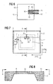
- FIG. 7 shows a plan view of this known pressure sensor. A sectional drawing of this pressure sensor along the section line A - A 'is in FIG. 8 shown.
- the pressure sensor is fabricated on a silicon substrate 2 having a (100) orientation.
- a membrane 10 On the underside of a membrane 10 is a truncated pyramid-shaped depression. Their shape is such that only silicon material of a small residual thickness, the membrane 10, remains at the location of the truncated pyramid.
- the boundary lines of the truncated pyramid are in FIG. 7 dashed lines and are parallel to the [110] and [1 1 0] directions, whose course in FIG. 7 is indicated by the arrows 40 and 41 respectively.
- the non-thinned part of the silicon substrate 2 is also called carrier 11.
- a measuring resistor 4 which runs in the [110] direction.
- a compensation resistor 5 Perpendicular to the direction of the measuring resistor 4, running in [110] direction, located at the left electrode, a compensation resistor 5.
- the compensation resistor 5 is connected at one end via a connecting conductor 7 to the measuring resistor 4, with its other end via a second connecting conductor 7 with the electrode 6.
- the double arrows 30 and 31, 32 indicate mechanical stresses, which in explaining the operation This known pressure sensor come with hysteresis compensation to fruition.
- FIG. 8 shows a cross section through the pressure sensor 'from FIG. 7 ,
- the substrate 2 has a trapezoidal in cross-section depression, which is bounded by the carrier 11 and the membrane 10.
- the measuring resistor 4 is located in the surface of the membrane 10.
- the measuring resistor 4 is realized by introducing a local doping zone into the silicon material.
- the operation of the known pressure sensor with hysteresis compensation is the following.
- a pressure acting from the outside on the pressure sensor pressure of the pressure sensor is mechanically deformed.
- the thickness of the carrier 11 is typically several 100 microns, while the thickness of the membrane 10 is typically several microns. Because of the different stiffnesses resulting therefrom, the mechanical deformation in the carrier 11 is negligible compared to the mechanical deformation in the diaphragm.
- the resulting from the pressure applied from the outside stress or deformation is illustrated by an arrow 31, the length of which is a measure of the deformation.
- the mechanical deformation is exemplified at one point, namely at the location of the measuring resistor 4.
- a first deformation 30 is present, the cause of which is a mechanical interference voltage, which in the present case to the different thermal Expansion coefficient of the aluminum of the electrodes and silicon of the substrate 2 is based.
- Each point in the pressure sensor can be assigned such a first mechanical stress or deformation 30, but only two points in the pressure sensor should be considered. These two points are the location of the measuring resistor 4 and the location of the compensation resistor 5.
- the first deformation 30 is the same everywhere.
- the measuring resistor 4 and the compensation resistor 5 are dimensioned so that their piezoresistive coefficients are equal in magnitude. Similarly, the absolute values of the electrical resistance are the same under the same external conditions. Thus, the changes in the electrical resistance value in the measuring resistor 4 and in the compensation resistor 5 due to the first deformation 30 are equal in magnitude. However, once the resistance is arranged in the direction of deformation and once perpendicular to the deformation, the two resistance changes have a different sign. The total resistance change of the equivalent resistance for the series connection of measuring resistor 4 and compensation resistor 5 due to the first deformation 30 is thus 0. Thus, only the change of the measuring resistor due to the second deformation 31, which is the compensation resistor 5, which is located on the carrier 11 is not is exposed.
- a disadvantage of the above known hysteresis compensation solution has been found to be the fact that that it has only a low efficacy and leads to a loss of sensitivity.
- a hysteresis of the output signal above the temperature generally occurs on the transducer element without compensation.
- Fig. 9 illustrates this hysteresis of stress as a function of temperature
- Fig. 10 shows the hysteresis of another known pressure sensor without compensation as a function of the membrane edge length mk for different internal circuit radii SIR.
- the circuit conductors of the evaluation circuit completely enclose the membrane.
- the chip size is 4 mm. In the area of negative hysteresis the global effect outweighs, in the area of positive hysteresis the edge effect.
- the hysteretic behavior of the entire aluminum wiring of the evaluation circuit has an integral long-distance effect on the piezoresistors of the transducer element, by a "bimetallic deformation" (aluminum layer on silicon) of the entire sensor element (global effect) and by a local effect at a distance of the circuit edge to piezoresistor 100 ⁇ m (edge effect).
- the hysteresis of the solder should therefore be taken into account for the absolute hysteresis calculation.
- micromechanical pressure sensor which, depending on the type, are located in the region in which the edge effect or the global effect predominates. They become a Wheatstone bridge interconnected, whose output signal logically also has a temperature hysteresis. This temperature hysteresis superimposes the actual sensor signal.
- a semiconductor pressure sensor having a strain gauge on a diaphragm portion is known.
- stress compensation films are provided on the membrane portion.
- micromechanical component according to the invention with the features of claim 1 and the adjustment method according to claim 7 or 8 have the advantage over known approaches that it has a high maximum compensation effect and a small minimum gradation.
- the compensation can be integrated into the circuit without any problems. An adjustment by mask programming can be provided. Alternatively, optimum compensation can be set on a precursor.
- the idea on which the present invention is based is that at least one spot made of such a material is provided in the surrounding area and / or in the membrane area such that a deformation of the spot or spots relative to the substrate results in an analogous Interference can be generated in such a way that the interference effect on the measuring resistor can be compensated.
- a compensation resistor device which is designed such that one or more compensation resistors can be connected to the measuring resistor, wherein respective spots are provided in the region of the compensation resistors.
- a positive or negative hysteresis is counteracted by switching on one or more compensation resistors as required.
- the addition of the compensation resistor or resistors is selectively carried out, so that from a predetermined number of compensation resistors a certain combination can be selected, which is to be added to the measuring resistor.
- This structure makes it possible to determine the exact compensation effect by separating printed conductors on the completely assembled sensor.
- the structure may also be designed so that a specific compensation effect can be set by a mask change.
- Selektiviereschaltbar means that by disconnecting traces a connection is interrupted or by Short circuiting of conductors creates a connection. This can be realized eg by burning distances (laser or voltage pulse) or by thyristor zapping. Thus, a single adjustment at the end of the tape for high-precision requirements is possible.
- one or more spots are provided in the membrane area, which act directly on the measuring resistor.
- one or more preferably annular spots are provided, which are located in the surrounding area between the diaphragm edge and the circuit inner radius of the evaluation circuit.
- a negative hysteresis is compensated by the thus controllable global effect. In this case, no compensation resistors are needed.
- Circuit inner radius means the step between the circuit area and the surrounding area (e.g., Al stage).
- the material of the patches is the conductor track material of the evaluation circuit.
- the spots are located above or alongside an associated compensation resistor.
- the substrate material is silicon and the conductor material aluminum.
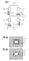
- Fig. 1 shows a section of a micromechanical pressure sensor as a first embodiment of the present invention.
- Fig. 1 4a designates two longitudinal measuring resistors and 4b two transversal measuring resistors, 60 spots of conductor material (here aluminum), 5a two compensating resistors of the transversal measuring resistors, 5b two compensating resistors of the longitudinal measuring resistors, V + and V- supply potentials and U a voltage output signal.
- Fig. 1 is only a schematic representation of the circuit arrangement and the measuring resistors 4a, 4b are on the membrane, while the compensation resistors 5a, 5b and associated spots 60 are arranged on the surrounding area (carrier).
- the general operating principle of the present first embodiment is to compensate for the hysteresis of the micromechanical pressure sensor by integrated into the supply line of the measuring resistors 4a, 4b, the compensation resistors 5a, 5b (about 80 microns outside the membrane).
- These are typically piezo-sensitive resistors, for example 200 ⁇ / square (size approx. 1 square, resistance approx. 200 ⁇ ), which are in series with the measuring resistors.
- the aluminum spots 60 lie transversely to the compensation resistors 5a and longitudinally to the compensation resistors 5b.
- an isolation level such as a SiO 2 layer, which has contact holes only at desired points and thus prevents unwanted short circuits.
- the hysteretic voltage difference acts perpendicular or parallel to the current direction. Since the longitudinal and transverse piezoelectric coefficients have different signs, both positive and negative hystereses can be generated at the compensation resistors 5a, b. This is referred to herein as active hysteresis compensation.
- the hysteresis strength induced for compensation purposes can be modified by the distance of the aluminum spots 60 to the compensation resistor 5a, 5b and their shape and size.
- the structure shown has a limited effectiveness, in particular, the effectiveness depends on the respective sensor type.
- the measuring bridge loses 10% of sensitivity. This is critical especially in the low pressure range.
- the sensitivity loss must be compensated by increasing the size of the membrane. This leads to an increase in nonlinearity, increases the risk of buckling and the cost. It is therefore preferable to compensate, which works without loss of sensitivity, or with the least possible loss of sensitivity.
- Fig. 2a, b shows a section of a micromechanical pressure sensor as a second embodiment of the present invention.
- This second embodiment relates to passive compensation of negative hysteresis without loss of sensitivity.
- Fig. 2a, b Denote 70, 70 'a respective electrically non-active metal spots of aluminum, which are used for compensation by exploiting the global effect.
- the basic hysteresis is negative (cf. Fig. 10 ).
- the additional trace material spots 70, 70 'at the circuit edge the electrically functionless are used exclusively because of their mechanical action.
- the patches 70, 70 ' are in annular form and are located on the surrounding area of the membrane 10, ie between the inner circuit radius and the diaphragm edge.
- the ring can be completely closed (compensation ring 70) or concentrate on the center of the membrane edges, since the effect is greatest in this area (compensation ring 70 '). In the latter case, more space is available for the evaluation circuit 50 in the corners.
- the passive compensation presented in this example has no effect on the sensitivity. However, it increases the cost as electrically inactive area is consumed. Alternatively, either a wide aluminum strip or many small strips can be used.
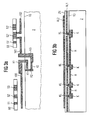
- Fig. 3a, b show a section of a micromechanical pressure sensor as a third embodiment of the present invention.
- This third embodiment relates to compensation positive hysteresis with the least possible loss of sensitivity.
- Fig. 3a, b denote in addition to the already introduced reference numerals K1, K2, K3 introduced into the substrate low-impedance supply areas, 41, 42 measuring resistors, 100, 101, 102 interconnects of aluminum and 51, 52, 53 and 51 ', 52', 53 'compensation resistors.
- active hysteresis compensation i.e., compensation resistor connected to, e.g., in series with, the sense resistor
- the arrangement is the most favorable, in which the absolute value of the compensation resistor is as low as possible, but the hysteresis of the resistance value as large as possible. This achieves maximum compensation with minimal loss of sensitivity.
- the respective compensation resistor 5a, b of 200 ⁇ is installed firmly in the overall bridge. This means a loss of sensitivity of 10% even in the event that the compensation is not necessary, i. the associated measuring resistor has no aluminum environment.
- the proposed structure according to the third embodiment consists of a respective series of compensation resistors 51, 52, 53 and 51 ', 52', 53 ', which can be connected alternatively or together in series with the measuring resistors 41, 42.
- the resistance values are eg 2x90 ⁇ (51, 51 '), 2x180 ⁇ (52, 52') and 2x360 ⁇ (53, 53 '). This corresponds eg to 0.5 square, 1 square and 2 square of the base resistance. In this case, the total resistance to be switched on is selected so that it is sufficient for the compensation.
- these compensation resistors 51, 52, 53 or 51 ', 52', 53 'connected in series to a transverse measuring resistor 41, 42 they have compensatory effect of the hysteresis in the negative direction. In the present case, only the 180 ⁇ (1 square) compensation resistor 52 'is connected. This can be done in final metering by removing unnecessary or adding desired traces (e.g., to generate short circuits) or at the mask programming stage. In the latter case, precursors with test wafers are recommended.
- Fig. 3b schematically follows the layer structure of the embodiment Fig. 3a out.
- K denotes the feed line area plane which lies in the region of the resistance plane.
- 13 is an insulator plane
- Al1 is a first interconnect level
- ZN is an intermediate nitride level
- Al2 is a second interconnect level for the patches 60.
- KL designates vias for connecting the contact plane K to the first interconnect level All. Not shown is an uppermost protective layer of nitride.
- the Al1 interconnects are short-circuited. Thus, the corresponding resistors are disabled. If the resistors are only needed in their electrical effect, Al2 is completely removed and Al1 is removed across the resistors, but remains as a contact terminal.
- Fig. 4 an investigation of the relative hysteretic resistance change at a temperature loop of -40 to 140 ° C, with the aluminum spot in a long strip over the compensation resistor in the direction of current
- Fig. 5 an analogous study in which the aluminum spot lies in a long strip along the compensation resistor in the current direction.
- b denote the width of the Al conductor, d zn the thickness of the intermediate nitride, d al the aluminum thickness and d ox the insulator thickness (here SiO 2 ).
- the resistor R is realized here by a p-diffusion into an n-substrate.
- Fig. 5 denote in addition to the already introduced reference numerals x the distance of the Al conductor to the resistor R, d sn the thickness of the protective nitride and d all / 2 the aluminum thicknesses of the two conductor layers.
- TKR and TK2R are corresponding constants.
- the transverse resistance R T has an analogous relationship.
- the example has been assumed to use both the Al1 and Al2 planes.
- the maximum achievable hysteretic stress (remanent stress) under the aluminum strip ie at the location of the compensation resistor 10MPa. If only the all-level is used, the stress is about 1/3 of this value.
- the compensation effect is reduced to 1/3.
- the finest compensation effect is less than 0.1% of the bridge hysteresis.
- Fig. 6 shows a section of a micromechanical pressure sensor as a fourth embodiment of the present invention.
- hysteresis compensation takes place directly on the sense resistor, i. the aluminum spots 60 are arranged to lie directly on the measuring resistors 41, 42. This allows for compensation even in the event that the original circuit inside radius already has a positive fundamental hysteresis (i.e., the circuit is already too close to the diaphragm edge).
- a compensation strip 60 would be placed longitudinally on the resistor, because this also produces a compressive stress, but parallel to the current direction.
- micromechanical device according to the invention has been described above with reference to preferred embodiments, it is not limited thereto, but modifiable in a variety of ways.
- the compensation of the hysteresis can be done in various ways. On the one hand, this can be done by mask programming, e.g. over the levels contact and metal, happen.
- the resistors are inherently under the oxide and are guaranteed to be inactive. They are only connected when needed.
- FIB Focus Ion Beam
- burning distances or thyristor zapping or oxide zapping the structure of test chips is designed so that it is possible to connect the compensation resistors by means of FIB cutting. This allows a quick optimization of the built-up sensor.
- the matching structures can also be integrated in the circuit part. This is even advantageous if an influence of the compensation resistances of the diaphragm edge is present.
Landscapes
- Physics & Mathematics (AREA)
- General Physics & Mathematics (AREA)
- Measuring Fluid Pressure (AREA)
- Pressure Sensors (AREA)
Claims (8)
- Composant micromécanique, en particulier sonde de pression, qui présente :- un substrat (2) qui présente une partie (10) en membrane et une partie qui entoure la partie (10) en membrane et- au moins une résistance variable de mesure (4a, 4b; 41, 42) formée dans la partie en membrane (10) par déformation de la partie en membrane (10) et- un circuit d'évaluation (50) approprié ménagé dans la partie environnante, une déformation de parties, en particulier de pistes conductrices, du circuit d'évaluation (50) par rapport au substrat (2) permettant d'exercer une influence perturbatrice sur la résistance de mesure (4a, 4b; 41, 42) et- au moins une tache (60; 70, 70') prévue dans la partie environnante et/ou dans la partie en membrane (10), en un matériau tel qu'une déformation de la ou des taches (60) par rapport au substrat (2) permet d'exercer une influence perturbatrice analogue qui permet de compenser l'influence perturbatrice qui agit sur la résistance de mesure (4a, 4b; 41, 42),caractérisé par- un système à résistance de compensation configuré de manière à pouvoir ajouter une ou plusieurs résistances de compensation à la résistance de mesure (4a, 4b; 41, 42) et- par des taches (60) prévues au-dessus ou le long d'une résistance de compensation associée (5a, 5b; 51, 52, 53, 51', 52', 53').
- Composant micromécanique selon la revendication 1, caractérisé en ce que le raccordement supplémentaire de la ou des résistances de compensation (5a, 5b; 51, 52, 53, 51', 52', 53') peut être réalisé sélectivement de sorte qu'à partir d'un nombre prédéterminé de résistances de compensation, on puisse sélectionner une combinaison définie qui est ajoutée à la résistance de mesure.
- Composant micromécanique selon les revendications 1 ou 2, caractérisé en ce qu'une ou plusieurs taches (60) sont prévues dans la partie en membrane (10) pour agir directement sur la résistance de mesure (41, 42).
- Composant micromécanique selon l'une des revendications précédentes, caractérisé en ce qu'une ou plusieurs taches (70, 70'), de préférence de forme annulaire, sont prévues et sont situées dans la partie environnante, entre le bord (15) de la membrane et le rayon intérieur du circuit d'évaluation (50).
- Composant micromécanique selon l'une des revendications précédentes, caractérisé en ce que le matériau des taches (60; 70, 70') est le matériau des pistes conductrices du circuit d'évaluation (50).
- Composant micromécanique selon l'une des revendications précédentes, caractérisé en ce que le matériau du substrat est le silicium et le matériau des pistes conductrices l'aluminium.
- Procédé d'équilibrage d'un composant micromécanique selon la revendication 2, dont le raccordement supplémentaire sur une puce de test est optimisé.
- Procédé d'équilibrage d'un composant micromécanique selon la revendication 2, dont le raccordement supplémentaire est optimisé en un équilibrage final distinct.
Applications Claiming Priority (3)
| Application Number | Priority Date | Filing Date | Title |
|---|---|---|---|
| DE10013904 | 2000-03-21 | ||
| DE10013904A DE10013904A1 (de) | 2000-03-21 | 2000-03-21 | Mikromechanisches Bauelement und Abgleichverfahren |
| PCT/DE2001/000992 WO2001070625A2 (fr) | 2000-03-21 | 2001-03-15 | Composant micromecanique et procede d'equilibrage |
Publications (2)
| Publication Number | Publication Date |
|---|---|
| EP1277033A2 EP1277033A2 (fr) | 2003-01-22 |
| EP1277033B1 true EP1277033B1 (fr) | 2009-09-23 |
Family
ID=7635718
Family Applications (1)
| Application Number | Title | Priority Date | Filing Date |
|---|---|---|---|
| EP01923518A Expired - Lifetime EP1277033B1 (fr) | 2000-03-21 | 2001-03-15 | Composant micromecanique et procede d'equilibrage |
Country Status (5)
| Country | Link |
|---|---|
| US (1) | US6782756B2 (fr) |
| EP (1) | EP1277033B1 (fr) |
| JP (1) | JP4921674B2 (fr) |
| DE (2) | DE10013904A1 (fr) |
| WO (1) | WO2001070625A2 (fr) |
Families Citing this family (3)
| Publication number | Priority date | Publication date | Assignee | Title |
|---|---|---|---|---|
| US7055392B2 (en) * | 2003-07-04 | 2006-06-06 | Robert Bosch Gmbh | Micromechanical pressure sensor |
| TWI265555B (en) * | 2005-08-23 | 2006-11-01 | Touch Micro System Tech | Method of forming a piezoresistive device capable of selecting standards and method of forming a circuit layout capable of selecting sub circuit layouts |
| DE102017114299A1 (de) * | 2017-06-28 | 2019-01-03 | Endress+Hauser SE+Co. KG | Verfahren zur Herstellung einer Druckmesseinrichtung |
Family Cites Families (13)
| Publication number | Priority date | Publication date | Assignee | Title |
|---|---|---|---|---|
| US4333349A (en) * | 1980-10-06 | 1982-06-08 | Kulite Semiconductor Products, Inc. | Binary balancing apparatus for semiconductor transducer structures |
| JPS59217375A (ja) * | 1983-05-26 | 1984-12-07 | Toyota Central Res & Dev Lab Inc | 半導体機械−電気変換装置 |
| DE3319605A1 (de) * | 1983-05-30 | 1984-12-06 | Siemens AG, 1000 Berlin und 8000 München | Sensor mit polykristallinen silicium-widerstaenden |
| US4682503A (en) * | 1986-05-16 | 1987-07-28 | Honeywell Inc. | Microscopic size, thermal conductivity type, air or gas absolute pressure sensor |
| US4726232A (en) * | 1986-06-02 | 1988-02-23 | Gould Inc. | Temperature coefficient compensated pressure transducer |
| JP3114453B2 (ja) * | 1993-10-05 | 2000-12-04 | 株式会社日立製作所 | 物理量検出センサ及びプロセス状態検出器 |
| DE4415984A1 (de) * | 1994-05-06 | 1995-11-09 | Bosch Gmbh Robert | Halbleitersensor mit Schutzschicht |
| JP3319173B2 (ja) * | 1994-09-19 | 2002-08-26 | 株式会社日立製作所 | センサ |
| DE19517676B4 (de) * | 1995-05-13 | 2008-01-31 | Robert Bosch Gmbh | Drucksensor für eine Brennkraftmaschine mit einem Ansaugrohr |
| DE19701055B4 (de) | 1997-01-15 | 2016-04-28 | Robert Bosch Gmbh | Halbleiter-Drucksensor |
| DE19731420A1 (de) * | 1997-07-22 | 1999-01-28 | Bosch Gmbh Robert | Vorrichtung zur Erfassung des Drucks und der Temperatur im Saugrohr einer Brennkraftmaschine und Verfahren zu ihrer Herstellung |
| JP3873454B2 (ja) * | 1998-05-29 | 2007-01-24 | 株式会社デンソー | 半導体圧力センサ |
| DE19825464A1 (de) * | 1998-06-08 | 1999-12-09 | Bosch Gmbh Robert | Vorrichtung zur Druckmessung |
-
2000
- 2000-03-21 DE DE10013904A patent/DE10013904A1/de not_active Withdrawn
-
2001
- 2001-03-15 JP JP2001568841A patent/JP4921674B2/ja not_active Expired - Fee Related
- 2001-03-15 US US10/239,470 patent/US6782756B2/en not_active Expired - Lifetime
- 2001-03-15 DE DE50115118T patent/DE50115118D1/de not_active Expired - Lifetime
- 2001-03-15 EP EP01923518A patent/EP1277033B1/fr not_active Expired - Lifetime
- 2001-03-15 WO PCT/DE2001/000992 patent/WO2001070625A2/fr not_active Ceased
Also Published As
| Publication number | Publication date |
|---|---|
| JP2004506522A (ja) | 2004-03-04 |
| JP4921674B2 (ja) | 2012-04-25 |
| DE50115118D1 (de) | 2009-11-05 |
| EP1277033A2 (fr) | 2003-01-22 |
| DE10013904A1 (de) | 2001-09-27 |
| WO2001070625A2 (fr) | 2001-09-27 |
| US20030150253A1 (en) | 2003-08-14 |
| WO2001070625A3 (fr) | 2002-10-24 |
| US6782756B2 (en) | 2004-08-31 |
Similar Documents
| Publication | Publication Date | Title |
|---|---|---|
| DE69126501T2 (de) | Kraftdetektor und Beschleunigungsdetektor | |
| DE19825761C2 (de) | Vorrichtung zum Erfassen einer Dehnung und/oder einer Stauchung eines Körpers | |
| DE19701055B4 (de) | Halbleiter-Drucksensor | |
| DE69602483T2 (de) | Kraftwandler und Herstellungsverfahren dazu | |
| DE112017000422T5 (de) | Kraft- / drehmomentsensor mit instrumentierung auf weniger als vierträgeroberflächen | |
| EP1380825A1 (fr) | Capteur de pression microméchanique et ensemble de mesure correspondant | |
| DE4130044A1 (de) | Halbleiter-drucksensor | |
| DE19948045A1 (de) | Sitzgewichtsmeßvorrichtung | |
| EP1876434A2 (fr) | Dispositif destiné à la mesure de forces, en particulier un capteur de pression, et procédé de fabrication correspondant | |
| EP0526600B1 (fr) | Capteur de pression pour la mesure de pression dans la chambre d'explosion d'un moteur a combustion interne | |
| DE69310678T2 (de) | Mikromechanisch hergestellter Messaufnehmer | |
| CH664235A5 (de) | Piezoelektrisches messelement. | |
| DE69008225T2 (de) | Druckwandler der Art Halbleiter auf Isolierschicht. | |
| DE112011105592B4 (de) | Halbleitereinrichtung und Verfahren zur Herstellung derselben | |
| DE102019129411A1 (de) | Aufnehmerkörper mit einem Messelement und Herstellungsverfahren für einen Aufnehmerkörper | |
| DE19957556A1 (de) | Halbleiter-Drucksensor und Meßanordnung | |
| EP1277033B1 (fr) | Composant micromecanique et procede d'equilibrage | |
| DE2940955C2 (fr) | ||
| EP0342274B1 (fr) | Agencement pour réduire des effets piézo dans un matériel semi-conducteur comportant au moins un dispositif électrique à effet piézo et son procédé de fabrication | |
| EP3752809B1 (fr) | Assemblage pour une puce de capteur de pression à semi-conducteur et puce de capteur de pression | |
| DE112019006628T5 (de) | Halbleitervorrichtung und herstellungsverfahren dafür | |
| EP0992778A2 (fr) | Capteur et son procédé de fabricage | |
| DE102004023063A1 (de) | Mikromechanische piezoresistive Drucksensorenvorrichtung | |
| DE102017010404B4 (de) | Vibrationswandler | |
| DE10036495C2 (de) | Kraftmessvorrichtung in Form eines Biegebalkensensors |
Legal Events
| Date | Code | Title | Description |
|---|---|---|---|
| PUAI | Public reference made under article 153(3) epc to a published international application that has entered the european phase |
Free format text: ORIGINAL CODE: 0009012 |
|
| AK | Designated contracting states |
Kind code of ref document: A2 Designated state(s): AT BE CH CY DE DK ES FI FR GB GR IE IT LI LU MC NL PT SE TR |
|
| 17P | Request for examination filed |
Effective date: 20030424 |
|
| RBV | Designated contracting states (corrected) |
Designated state(s): DE FR GB IT |
|
| 17Q | First examination report despatched |
Effective date: 20080630 |
|
| GRAP | Despatch of communication of intention to grant a patent |
Free format text: ORIGINAL CODE: EPIDOSNIGR1 |
|
| GRAS | Grant fee paid |
Free format text: ORIGINAL CODE: EPIDOSNIGR3 |
|
| GRAA | (expected) grant |
Free format text: ORIGINAL CODE: 0009210 |
|
| AK | Designated contracting states |
Kind code of ref document: B1 Designated state(s): DE FR GB IT |
|
| REG | Reference to a national code |
Ref country code: GB Ref legal event code: FG4D Free format text: NOT ENGLISH |
|
| REF | Corresponds to: |
Ref document number: 50115118 Country of ref document: DE Date of ref document: 20091105 Kind code of ref document: P |
|
| PLBE | No opposition filed within time limit |
Free format text: ORIGINAL CODE: 0009261 |
|
| STAA | Information on the status of an ep patent application or granted ep patent |
Free format text: STATUS: NO OPPOSITION FILED WITHIN TIME LIMIT |
|
| 26N | No opposition filed |
Effective date: 20100624 |
|
| PGFP | Annual fee paid to national office [announced via postgrant information from national office to epo] |
Ref country code: FR Payment date: 20140319 Year of fee payment: 14 Ref country code: IT Payment date: 20140327 Year of fee payment: 14 |
|
| PGFP | Annual fee paid to national office [announced via postgrant information from national office to epo] |
Ref country code: GB Payment date: 20140324 Year of fee payment: 14 |
|
| GBPC | Gb: european patent ceased through non-payment of renewal fee |
Effective date: 20150315 |
|
| PG25 | Lapsed in a contracting state [announced via postgrant information from national office to epo] |
Ref country code: IT Free format text: LAPSE BECAUSE OF NON-PAYMENT OF DUE FEES Effective date: 20150315 |
|
| REG | Reference to a national code |
Ref country code: FR Ref legal event code: ST Effective date: 20151130 |
|
| PG25 | Lapsed in a contracting state [announced via postgrant information from national office to epo] |
Ref country code: GB Free format text: LAPSE BECAUSE OF NON-PAYMENT OF DUE FEES Effective date: 20150315 |
|
| PG25 | Lapsed in a contracting state [announced via postgrant information from national office to epo] |
Ref country code: FR Free format text: LAPSE BECAUSE OF NON-PAYMENT OF DUE FEES Effective date: 20150331 |
|
| REG | Reference to a national code |
Ref country code: DE Ref legal event code: R084 Ref document number: 50115118 Country of ref document: DE |
|
| PGFP | Annual fee paid to national office [announced via postgrant information from national office to epo] |
Ref country code: DE Payment date: 20200526 Year of fee payment: 20 |
|
| REG | Reference to a national code |
Ref country code: DE Ref legal event code: R071 Ref document number: 50115118 Country of ref document: DE |