EP1278070A2 - Procédé et dispositif à faible coût de détection de courant et de tension dans des circuits en fonction d'une chute de tension - Google Patents
Procédé et dispositif à faible coût de détection de courant et de tension dans des circuits en fonction d'une chute de tension Download PDFInfo
- Publication number
- EP1278070A2 EP1278070A2 EP02255019A EP02255019A EP1278070A2 EP 1278070 A2 EP1278070 A2 EP 1278070A2 EP 02255019 A EP02255019 A EP 02255019A EP 02255019 A EP02255019 A EP 02255019A EP 1278070 A2 EP1278070 A2 EP 1278070A2
- Authority
- EP
- European Patent Office
- Prior art keywords
- voltage
- resistor
- circuit
- coupled
- diode
- Prior art date
- Legal status (The legal status is an assumption and is not a legal conclusion. Google has not performed a legal analysis and makes no representation as to the accuracy of the status listed.)
- Withdrawn
Links
Images


Classifications
-
- G—PHYSICS
- G01—MEASURING; TESTING
- G01R—MEASURING ELECTRIC VARIABLES; MEASURING MAGNETIC VARIABLES
- G01R19/00—Arrangements for measuring currents or voltages or for indicating presence or sign thereof
- G01R19/165—Indicating that current or voltage is either above or below a predetermined value or within or outside a predetermined range of values
- G01R19/16566—Circuits and arrangements for comparing voltage or current with one or several thresholds and for indicating the result not covered by subgroups G01R19/16504, G01R19/16528, G01R19/16533
- G01R19/16571—Circuits and arrangements for comparing voltage or current with one or several thresholds and for indicating the result not covered by subgroups G01R19/16504, G01R19/16528, G01R19/16533 comparing AC or DC current with one threshold, e.g. load current, over-current, surge current or fault current
-
- G—PHYSICS
- G01—MEASURING; TESTING
- G01R—MEASURING ELECTRIC VARIABLES; MEASURING MAGNETIC VARIABLES
- G01R19/00—Arrangements for measuring currents or voltages or for indicating presence or sign thereof
- G01R19/165—Indicating that current or voltage is either above or below a predetermined value or within or outside a predetermined range of values
- G01R19/16504—Indicating that current or voltage is either above or below a predetermined value or within or outside a predetermined range of values characterised by the components employed
- G01R19/16523—Indicating that current or voltage is either above or below a predetermined value or within or outside a predetermined range of values characterised by the components employed using diodes, e.g. Zener diodes
-
- G—PHYSICS
- G01—MEASURING; TESTING
- G01R—MEASURING ELECTRIC VARIABLES; MEASURING MAGNETIC VARIABLES
- G01R31/00—Arrangements for testing electric properties; Arrangements for locating electric faults; Arrangements for electrical testing characterised by what is being tested not provided for elsewhere
- G01R31/40—Testing power supplies
-
- H—ELECTRICITY
- H02—GENERATION; CONVERSION OR DISTRIBUTION OF ELECTRIC POWER
- H02M—APPARATUS FOR CONVERSION BETWEEN AC AND AC, BETWEEN AC AND DC, OR BETWEEN DC AND DC, AND FOR USE WITH MAINS OR SIMILAR POWER SUPPLY SYSTEMS; CONVERSION OF DC OR AC INPUT POWER INTO SURGE OUTPUT POWER; CONTROL OR REGULATION THEREOF
- H02M3/00—Conversion of DC power input into DC power output
- H02M3/22—Conversion of DC power input into DC power output with intermediate conversion into AC
- H02M3/24—Conversion of DC power input into DC power output with intermediate conversion into AC by static converters
- H02M3/28—Conversion of DC power input into DC power output with intermediate conversion into AC by static converters using discharge tubes with control electrode or semiconductor devices with control electrode to produce the intermediate AC
- H02M3/325—Conversion of DC power input into DC power output with intermediate conversion into AC by static converters using discharge tubes with control electrode or semiconductor devices with control electrode to produce the intermediate AC using devices of a triode or a transistor type requiring continuous application of a control signal
- H02M3/335—Conversion of DC power input into DC power output with intermediate conversion into AC by static converters using discharge tubes with control electrode or semiconductor devices with control electrode to produce the intermediate AC using devices of a triode or a transistor type requiring continuous application of a control signal using semiconductor devices only
- H02M3/33507—Conversion of DC power input into DC power output with intermediate conversion into AC by static converters using discharge tubes with control electrode or semiconductor devices with control electrode to produce the intermediate AC using devices of a triode or a transistor type requiring continuous application of a control signal using semiconductor devices only with automatic control of the output voltage or current, e.g. flyback converters
-
- G—PHYSICS
- G01—MEASURING; TESTING
- G01R—MEASURING ELECTRIC VARIABLES; MEASURING MAGNETIC VARIABLES
- G01R19/00—Arrangements for measuring currents or voltages or for indicating presence or sign thereof
- G01R19/0084—Measuring voltage only
-
- G—PHYSICS
- G01—MEASURING; TESTING
- G01R—MEASURING ELECTRIC VARIABLES; MEASURING MAGNETIC VARIABLES
- G01R19/00—Arrangements for measuring currents or voltages or for indicating presence or sign thereof
- G01R19/0092—Measuring current only
Definitions
- the present invention relates generally to circuits with voltage and current sensing and, more specifically, the present invention relates to current and voltage sensing in circuits with voltage drop.
- a TL431 which drives an opto-coupler feedback circuit to control the output voltage at a programmed value set by external resistors.
- a relatively high level of accuracy is needed at the output of the charger circuit in order to meet a lower accuracy at the load due to voltage drop in the output cable that connects the charger to the load (the electronic product).
- the voltage drop in the output cable reduces the output voltage as load increases degrading the overall voltage tolerance at the load.
- a required level of voltage accuracy at the charger output can be achieved by choosing a TL431 IC that has been trimmed to the appropriate accuracy level. TL431s with 3%, 2% and 1% accuracy are widely available.
- TL431 voltage reference is generally more expensive than a simple zener reference.
- zeners are generally difficult to get at tolerance below 2% and the zener voltage varies with the current through it, resulting in a poorer load regulation in circuits that have zener currents that vary with output load due to low gain of the feedback loop.
- they are only available in certain standard voltage values, which makes it difficult to center the output voltage at the optimum point for the best tolerance.
- the current sensing in low power applications is usually done by using a voltage drop across a current sense resistor to turn on a bipolar a transistor.
- This circuit uses the base emitter voltage, V BE of the transistor as a reference.
- the transistor in turn drives an optocoupler feedback circuit to control the output current at a constant value.
- the constant current limit set by such a circuit however, has a large temperature variation due to the high temperature coefficient of V BE (-2mV/°C). This can be compensated to the first order by using a thermister based resistor network which add to the component count and cost.
- a circuit comprising:
- a circuit comprising:
- a circuit comprising:
- a circuit comprising:
- a circuit comprising:
- a circuit comprising:
- a seventh aspect of the invention there is provided a method, comprising:
- a current sense circuit including a series combination of a diode and a resistor in the path of the current to be sensed, the voltage across this series combination coupled to drive a light emitting diode (LED).
- the LED is part of an optocoupler and the optocoupler is part of a feedback circuit of a switched mode power supply.
- the diode is a PN junction diode.
- a current and voltage sense circuit including a current sense circuit having a series combination of a diode and a resistor in the path of a load current supplied from an output and the voltage across this series combination is coupled to drive an LED.
- the current and voltage sense circuit also includes a voltage sense circuit coupled to the output.
- the voltage sense circuit includes a voltage reference coupled to the base of a bipolar transistor. The bipolar transistor drives the LED when the voltage at the output exceeds a sense voltage of the voltage sense circuit.
- the voltage reference is a zener and the sense voltage of the voltage sense circuit is the sum of the voltage across the zener and the forward base emitter voltage (V BE ) of the bipolar transistor.
- the LED is part of an optocoupler and the optocoupler is part of a feedback circuit of switched mode power supply.
- the diode is a PN junction diode.
- a voltage drop compensation circuit including a voltage sense circuit coupled across a voltage output.
- the voltage sense circuit includes a voltage reference coupled to drive the base of the bipolar transistor when the voltage at the voltage output exceeds a sense voltage of the voltage sense circuit.
- a compensation resistor is coupled to the voltage output to carry a current that substantially represents the current that flows from the voltage output to a load that is coupled to the output.
- the sum of the voltage across the compensation resistor and the forward base emitter voltage of the bipolar transistor is applied across a series combination of a second resistor and a diode.
- the current through the second resistor is used to alter the sense voltage of the voltage sense circuit.
- the sense voltage is increased as the current to the load increases.
- the diode is replaced by a short circuit.
- the voltage reference is a zener and the sense voltage of the voltage sense circuit is the sum of the voltage across the zener and the forward base emitter voltage (V BE ) of the bipolar transistor and, the current through the second resistor is passed through the zener.
- the voltage sense circuit further includes a third resistor and the sense voltage is the sum of the voltage across the voltage reference, the voltage across the third resistor and the forward emitter bias voltage of the bipolar transistor and, the current through the second resistor is passed through the third resistor.
- the diode is a PN junction diode.
- the bipolar transistor drives an LED of an optocoupler and the optocoupler is part of a feedback circuit of switched mode power supply.
- a voltage drop compensation circuit which includes a voltage sense circuit coupled across a voltage output.
- the voltage sense circuit includes a first resistor coupled to a zener, which is coupled to drive an LED of an optocoupler when the voltage at the voltage output exceeds a sense voltage of the voltage sense circuit.
- the sense voltage of the voltage sense circuit is the sum of the voltage across the zener and the forward voltage of the optocoupler LED and the voltage across the first resistor.
- the voltage sense circuit also includes a current sense circuit, which provides a voltage representative of current delivered to a load coupled to the voltage output.
- the voltage sense circuit also includes a voltage compensation circuit coupled to change the voltage across the first resistor of the voltage sense circuit responsive to the voltage provided by the current sense circuit.
- the voltage across the first resistor is increased as the current supplied to the load increases.
- the current sense circuit includes a series combination of a second resistor and a diode.
- the voltage compensation circuit includes a third resistor coupled to the emitter of a bipolar transistor and a series combination of the third resistor and a base emitter junction of the bipolar transistor is coupled across the current sense circuit, such that the collector current of the transistor is proportional to the voltage across the second resistor.
- the bipolar transistor collector is coupled to the first resistor such that the voltage drop across the first resistor is responsive to the voltage across the second resistor.
- the optocoupler is part of a feedback circuit of switched mode power supply. Additional features and benefits of the present invention will become apparent from the detailed description and figures set forth below.
- Embodiments of methods and apparatuses for providing current sensing, voltage sensing and voltage drop compensation in circuits are disclosed.
- numerous specific details are set forth in order to provide a thorough understanding of the present invention. It will be apparent, however, to one having ordinary skill in the art that the specific detail need not be employed to practice the present invention. In other instances, well-known materials or methods have not been described in detail in order to avoid obscuring the present invention.
- embodiments of the present invention provide a very low cost, constant voltage, constant current sensing circuit that is relatively temperature independent.
- a cable resistance compensation circuit in accordance with one embodiment increases accuracy of the voltage at the load by compensating for the cable voltage drop. This also allows a lower cost voltage sense circuit to be used.
- a current sense circuit according to one embodiment can also be used for detecting the sensed current crossing a threshold for monitoring and protection purposes.
- One embodiment the present invention can be used to provide a relatively accurate, temperature compensated constant voltage and current characteristic for battery chargers.
- One of the described embodiments of the present invention uses zener based voltage sense for low cost.
- the reduced accuracy of the zener sensing is compensated for by a novel voltage drop compensation technique.
- This technique increases the sense voltage as a function of load to compensate for cable voltage drop and any change in zener voltage due to load related change in zener current.
- the net effective voltage accuracy measured at the load with this circuit is comparable to more expensive TL431 based circuits.
- the voltage drop compensation circuit could also be used in combination with more accurate voltage sense circuits such as the ones based on TL431 IC, to compensate for resistive drops in the conductors (wires, cables, printed circuit board traces, etc.) that connect the load to the voltage sense point, to further improve regulation accuracy at the load.
- the current sensing is done by using the forward voltage of the Light Emitting Diode (LED) as a voltage reference.
- the current is sensed by a series combination of a PN junction diode and a resistor and the voltage developed by this series combination is applied across the LED.
- This circuit takes advantage of the fact that the LED forward voltage has a temperature coefficient that is similar to that of the PN junction diode, but its absolute value is approximately 300 mV higher than that of the PN junction diode; i.e. a forward voltage of approximately 1V for LED vs. 0.7V for the PN junction diode.
- the voltage across the sense resistor in one embodiment is 300 mV and is relatively independent of temperature.
- this current sense circuit provides a relatively temperature independent constant current output using LED of an optocoupler in a closed loop feedback circuit.
- An added advantage of this circuit is that it provides constant current all the way down to a short circuit at the output. This is because the optocoupler LED is always driven in the constant current mode, independent of the output voltage.
- the simple low cost current sense circuit disclosed can also be used in an open loop fashion to detect a current crossing a threshold for monitoring and protection purposes, such as, over-current or overload detection, under-current or light load detection, over current shutdown, etc.
- the crossing of current threshold can be detected by the turn on (when current cross above the threshold) and turn off (when current crosses below the threshold) of the output transistor of the optocoupler.
- a stand alone LED can be used to visually indicate a current crossing a threshold.
- the LED on a power supply could light up to indicate that a power supply is loaded or over loaded.
- embodiments of the presently described current sense circuit a relatively temperature independent current threshold is obtained with a circuit that is very simple and low cost.
- embodiments of the present invention are described herein with a switched mode power supply, it is noted that other embodiments of the present invention are not limited in use to switched mode power supplies or even to power supplies in general.
- the embodiments of the present invention can be used for sensing voltage and current in linear power supplies, instrumentation systems that have remote sensors, monitoring of current or voltage crossing a set threshold, etc.
- Embodiments of the present invention can be used in a open loop system for monitoring voltage or current or in a closed loop system for regulation of voltage or current.
- Figure 1 shows a switched mode AC to DC power supply 101with CC/CV output coupled to a load 103 through a cable 105 having resistances of RC1 107 and RC2 109 in the positive and negative conductors respectively.
- This circuit uses one embodiment of the novel current sense, voltage sense and voltage drop compensation circuit according to the teachings of the present invention (shown within dotted lines) on the secondary side 129 of the transformer T1 111. The circuit operates in closed loop, to provide a relatively accurate constant current, constant voltage output.
- R1 113 is a fusible resistor that acts like a fuse for protecting the power supply 101 from component shorts and overloads.
- RV1 115 is a metal oxide varistor (MOV) used to clamp AC line transient from damaging the power supply.
- Diodes D1-D4 form a rectifier bridge 117 to convert AC to DC and the capacitors C1 119 and C2 121 smooth the DC voltage.
- C1 119 and C2 121 in combination with inductor L1 123 also provide electromagnetic interference (EMI) filtering for high frequency noise that is generated by the switching power supply 101 to limit conducted emission transmitted on to the AC line.
- U1 125 is a switched mode power supply controller with an integrated high voltage switch.
- U1 125 is a TNY264 device, which is a member of TINYSwitch II family of switched mode power supply ICs manufactured by Power Integrations of San Jose, California.
- Power supply controller 125 converts the high voltage DC across C2 121 into high frequency AC across the primary winding 127 (terminals 1 and 4) of the transformer T1 111.
- the amount of power delivered to the secondary terminals 129 (8 & 10) of T1 111 is controlled in closed loop through the EN/UV pin of the power supply controller 125.
- An optocoupler U2 131 is used to provide the feedback with isolation from the secondary side 129 of transformer 111 for closed loop control.
- elements R1 133, R2 135, D5 137 and C3 139 clamp leakage inductance spikes across the primary winding 127 of transformer T1 111.
- C4 141 is a bypass capacitor for the power supply controller 125 internal supply pin.
- D6 143 provides rectification and C5 145 provide filtering on the secondary 129 to deliver a DC voltage across C5 145.
- the circuit enclosed by the dotted line box in Figure 1 on the secondary side 129 of transformer T1 111 is one embodiment of a current sense, voltage sense and voltage drop compensation circuit 147 in accordance with the teachings of the present invention that is shown separately in Figure 2 for clarity.
- L2 149 and C6 151 is a high frequency post filter for reducing switching frequency ripple at the DC output terminals.
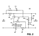
- FIG. 2 shows one embodiment of a current and voltage sense circuit 147 with voltage drop compensation in accordance with the teachings of the present invention used in the power supply of Figure 1.
- the DC input terminals are coupled across C5 145 on the secondary winding 129 side of transformer T1 111 of Figure 1.
- the DC output terminals are coupled through the high frequency post filter (L2 149 and C6 151 ) and a cable 105 having a resistance RC1 107 and RC2 109, on positive and negative rails respectively, to the load 103.
- a high frequency post filter (L2 149, C6 151) that is shown in Figure 1 has very little effect, if any, on the DC voltages and currents that are passed though directly to the cable 105. If L2 149 in Figure 1 introduces any significant series resistance, this could be lumped with the cable resistances RC1 107 for voltage drop compensation purposes. So, for the discussion that. follows, the post filter is assumed to be transparent to DC voltages and currents.
- R5 153, R6 155, D7 157 and optocoupler LED 159 constitute the current sense circuit.
- the voltage sense circuit includes PNP transistor Q1 161, R8 163, R9 165 and zener D8 167.
- zener D8 167 provides a voltage reference for the voltage sense circuit.
- the voltage drop compensation for the voltage sense circuit is performed by R3 169, R4 171, D9 173 in conjunction with R8 163.
- R6 155 and D7 157 are the current sensing components in return path of the current on the negative rail coupled to the DC output.
- the current through R6 155 and D7 157 is substantially equal to the load 103 current I L , which is supplied from the DC output and flows through the load 103 coupled to the DC output.
- the voltage dropped across R6 155 and D7 157 is applied across the LED 159 of the optocoupler 131 through the resistor R5 153, which limits the LED 159 current during the constant current mode of operation.
- R5 also limits the current that would flow through R6 155 and D7 157 when in the constant voltage mode of operation.
- the LED 159 of the optocoupler 131 conducts. This in turn reduces the power delivered by the power supply controller 125 to the transformer 111 to maintain the output current in regulation at the current sense threshold.
- the estimated value of R6 155 required for the constant current output of 600 mA is 300mV/600 mA, which equals 0.5 ohms. It is noted that the value of 0.51 ohms for R6 155 shown in Figure 1 was determined empirically for optimum positioning for one embodiment for the constant current value within the specification limits.
- the output voltage is regulated at a sense voltage that is the sum of the zener D8 167 voltage, base emitter voltage V BE of Q1 161, which is approximately 0.7V, and any voltage drop across resistor R8 163 that is generated by the voltage drop compensation circuit.
- R9 165 provides constant bias current through the zener D8 167 to reduce its dynamic impedance.
- the transistor Q1 161 conducts and drives the LED 159 of the optocoupler 131 to reduce the power delivered by the power supply controller 125 to the transformer 111 to maintain the output voltage in regulation at the sense voltage.
- R3 169 is the compensation resistor that is on the positive rail coupled to the DC output and has a current that is substantially equal to load 103 current I L .
- the voltage developed across R3 169 is substantially equal to the voltage across the resistor R4 171 independent of temperature because the forward voltage drop of diode D9 173 and the V BE of the transistor Q1 161 and their temperature coefficients are substantially the same in one embodiment. This is because both are PN junctions. Therefore, the current generated by R4 171 is proportional to the load current I L and flows through R8 163.
- the base current of Q1 161 by design is negligible compared to the current through R4 171. Therefore, the voltage drop across R8 163 is proportional to the load 103 current I L .
- the R3 169 value was chosen to drop a voltage at full load of 600 mA that is substantially larger than any component to component variation of differences in the diode D9 173 forward voltage and the V BE of Q1 161.
- the component voltage drop variations for PN junction diodes is in the order of 20mV. Accordingly, assuming that a voltage drop 10 times larger is chosen ( e.g. 200 mV), the value of R3 169 is 200 mV/600 mA, which equals 0.33 ohms. This value also has to be sufficient to provide the required voltage drop compensation at full load.
- R4 171 value of 120 ohms is chosen to provide a current as a function of load 103 that is much larger than the base current of Q1 161. At full load the current through R4 171 is 200 mV/ 120 ohms, which is equal to 1.67 mA. This means the R4 171 current will range from close to 0 mA at no load to 1.67 mA at full load.
- the value of R8 163 is then chosen to provide sufficient drop at full load to increase in sense voltage by an amount that is sufficient to compensate for the resistive voltage drops in the cable 105 coupled to the DC output.
- the R8 163 value chosen is 330 ohms, which changes the sense voltage by 1.67 mA x 330 ohms, which equals 0.55 V. This will provide compensation for a cable 105 resistance of approximately 0.55V/600 mA, which equals 0.9 ohms.
- the calculations above neglect the change in zener D8 167 voltage with current due to its internal impedance, which is usually small compared to 330 ohms.
- the actual value of R8 163 can be fine tuned empirically accounting for second order effects of the circuit to provide a substantially constant voltage output from no load to full load as measured at the load.
- the collector current of Q1 161 is the sum of LED 159 current, which in one embodiment is approximately 250 uA for driving power supply controller 125 devices independent of loading, and the current through R5 153.
- the current though R5 153 is maximum at no load and it can be estimated by dividing the voltage difference between the forward drop of the LED 159 of the optocoupler 131 and the PN junction diode D7 157 by the resistor value of R5 153, which is: 300 mV/100 ohms, which equals 3 mA. This is because the drop across the resistor R6 155 is negligible at no load.
- the total maximum Q1 161 current in one embodiment is 3,25 mA.
- the base current of Q1 161 is approximately 33 uA which translates to 33 uA X 330 ohms, which equals 10 mV across R8 163 at no load. This is negligible compared to the output voltage of 5.7V.
- a standard 4.7V zener diode D8 167 is biased close to 5V by the current through R9 165 of 0.7V/180 ohms, which equals 3.9 mA to center the output voltage at 5V + V R8 (0V) + V BE (0.7V), which equals 5.7Vat no load.
- resistor R8 163 it is possible to eliminate the resistor R8 163 by using zener diode D8 167 internal impedance to perform the function of R8 163.
- the value of R4 171 can be adjusted to provide the required change in zener D8 167 current to provide the change in sense voltage at full load.
- D9 173 it is also possible to eliminate D9 173 and use a correspondingly larger value of R4 171 to save cost.
- the voltage across R4 171 will then be equal to the drop across R3 169 plus a V BE (approximately 0.7V at room temperature) and the value of R4 171 can be chosen to provide the desired amount of voltage compensation at room temperature.
- the voltage across R4 171 will vary with temperature due to the V BE temperature coefficient of approximately-2 mV/°C. This will change the voltage compensation as a function of temperature that may be acceptable in some cases and desirable in some others.
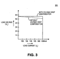
- Figure 3 shows one embodiment of the IV (current vs. voltage) characteristics 301 at the load for the circuit in Figure 1.
- the dotted line shows how the load voltage V L would drop with increasing load current, due to the cable resistance, if there were no voltage drop compensation.
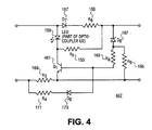
- Figure 4 shows another embodiment of a circuit 447 in accordance with the teachings of the present invention that is a complementary version of the circuit 147 in Figure 2.
- This circuit uses a NPN transistor Q1 461 instead of a PNP transistor Q1 161 used in Figures 1 and 2. This requires that the current sensing is done on the positive rail coupled to the DC output and the voltage drop compensation is done on the negative rail.
- the component numbers shown in Figure 4 match with the equivalent components shown in Figure 2. The operation and performance of the circuits are otherwise identical to the circuit in Figure 2.
- FIG. 5 shows another embodiment of a novel current sense, voltage sense and voltage drop compensation circuit 557 according to the teachings of the present invention.
- the DC input terminals are coupled across capacitor C5 145 on the secondary winding 129 side of transformer T1 111 of Figure 1.
- the DC output terminals are coupled through a high frequency post filter (L2 149 and C6 151) and a cable 105 having a resistance RC1 107 and RC2 109 as shown in Figure 1, on positive and negative rails respectively, to the load 103.
- R1 575, R2 577, D1 579 and the optocoupler LED 581 constitute the current sense circuit.
- the voltage sense circuit includes R3 583, D2 585 and the optocoupler LED 581.
- the voltage compensation circuit includes Q1 587 and R4 589. The operation of the current sense circuit is identical to that described in Figure 1.
- the output voltage is regulated at a sense voltage that is the sum of the voltage across zener D2 585, the optocoupler LED 581 forward voltage drop and the voltage across R3 583 minus the voltage across R1 575 and D1 579 forward voltage drop.
- R2 577 limits the current through the optocoupler LED 581 when it is being driven by the current sense circuit (constant current mode).
- R2 577 also provides bias current for zener D2 585 when the circuit is in a voltage sensing mode or constant voltage mode.
- the voltage drop compensation is achieved by increasing the current through R3 583 in response to increased output load 103 current I L .
- This function is achieved through the coupling of the base emitter junction of Q1 587 in series with R4 589, in parallel to R1 575 and D1 579.
- the voltage drop across R1 575 is representative of the output load 103 current I L .
- the voltage drop across D1 579 is substantially equal to the base emitter drop of Q1 587 and has the same temperature coefficient providing temperature compensation.
- the voltage across R1 575 is therefore substantially equal to the voltage across R4 589 independent of temperature.
- R4 589 therefore determines the Q 587 collector current for a given output load 103 current I L and hence the relationship between the voltage drop across R3 583 and the output load 103 current I L .
- R4 589 is chosen to compensate for both the voltage drop across R1 575 and the voltage drop due to cable 105 resistance, RC1 107 and RC2 109, of Figure 1.
- a complimentary version of the circuit shown in Figure 5 is constructed. This is similar to the complimentary versions of the same circuit shown in Figures 2 and 4.
- the complementary circuit embodiment uses a PNP transistor instead of an NPN transistor Q1 587 and the current sensing done on the positive rail coupled to the DC output.
- the voltage sense circuit would couple the optocoupler LED to the positive output rail in series with D2 585 and R3 583 coupled to the negative output rail with R4 589 coupled between the positive rail and the PNP transistor emitter.
- the operation and component choice is identical to the circuit of Figure 5 described above.
Landscapes
- Physics & Mathematics (AREA)
- General Physics & Mathematics (AREA)
- Engineering & Computer Science (AREA)
- Power Engineering (AREA)
- Computer Hardware Design (AREA)
- Microelectronics & Electronic Packaging (AREA)
- Dc-Dc Converters (AREA)
- Electronic Switches (AREA)
- Measurement Of Current Or Voltage (AREA)
Priority Applications (1)
| Application Number | Priority Date | Filing Date | Title |
|---|---|---|---|
| EP06013466A EP1750137A3 (fr) | 2001-07-20 | 2002-07-17 | Procédé et appareil à bas coût, circuits de captage de courant et de tension avec baisse de tension |
Applications Claiming Priority (4)
| Application Number | Priority Date | Filing Date | Title |
|---|---|---|---|
| US30671901P | 2001-07-20 | 2001-07-20 | |
| US306719P | 2001-07-20 | ||
| US10/188,583 US6795321B2 (en) | 2001-07-20 | 2002-07-03 | Method and apparatus for sensing current and voltage in circuits with voltage across an LED |
| US188583P | 2002-07-03 |
Related Child Applications (1)
| Application Number | Title | Priority Date | Filing Date |
|---|---|---|---|
| EP06013466A Division EP1750137A3 (fr) | 2001-07-20 | 2002-07-17 | Procédé et appareil à bas coût, circuits de captage de courant et de tension avec baisse de tension |
Publications (2)
| Publication Number | Publication Date |
|---|---|
| EP1278070A2 true EP1278070A2 (fr) | 2003-01-22 |
| EP1278070A3 EP1278070A3 (fr) | 2005-02-16 |
Family
ID=26884245
Family Applications (1)
| Application Number | Title | Priority Date | Filing Date |
|---|---|---|---|
| EP02255019A Withdrawn EP1278070A3 (fr) | 2001-07-20 | 2002-07-17 | Procédé et dispositif à faible coût de détection de courant et de tension dans des circuits en fonction d'une chute de tension |
Country Status (3)
| Country | Link |
|---|---|
| US (4) | US6795321B2 (fr) |
| EP (1) | EP1278070A3 (fr) |
| JP (2) | JP4150227B2 (fr) |
Cited By (6)
| Publication number | Priority date | Publication date | Assignee | Title |
|---|---|---|---|---|
| US7005914B2 (en) | 2001-07-20 | 2006-02-28 | Power Integrations, Inc. | Method and apparatus for sensing current and voltage in circuits with voltage across an LED |
| EP1720230A1 (fr) * | 2005-05-04 | 2006-11-08 | Power Integrations, Inc. | Alimentation de puissance avec circuit de détection de courant |
| WO2010144085A1 (fr) * | 2009-06-10 | 2010-12-16 | Semiconductor Components Industries, Llc | Procédé pour diminuer les pertes de puissance et circuit |
| CN104093245A (zh) * | 2014-07-03 | 2014-10-08 | 广东良得光电科技有限公司 | 一种高效隔离式led驱动电路 |
| CN101997433B (zh) * | 2009-08-13 | 2015-01-28 | 上海立隆微电子有限公司 | 反激电源转换器的二次侧电路 |
| DE102017209833A1 (de) * | 2017-06-12 | 2018-12-13 | Robert Bosch Gmbh | Vorrichtung zur Umformung elektrischer Energie und Verfahren zur Bestimmung eines durch ein elektronisches Bauelement fließenden Stroms |
Families Citing this family (69)
| Publication number | Priority date | Publication date | Assignee | Title |
|---|---|---|---|---|
| US7346785B2 (en) * | 1999-01-12 | 2008-03-18 | Microsemi Corp. - Analog Mixed Signal Group Ltd. | Structure cabling system |
| US7535735B2 (en) * | 2004-09-13 | 2009-05-19 | Power Integrations, Inc. | Compensation for parameter variations in a feedback circuit |
| DE602006020027D1 (de) | 2005-02-16 | 2011-03-24 | Leach Int Corp | Leistungsverteilungssystem unter verwendung von festkörperleistungsreglern |
| US20070024460A1 (en) * | 2005-08-01 | 2007-02-01 | Clark Richard L | Electrical apparatus with voltage drop indicator |
| US20070091529A1 (en) * | 2005-10-26 | 2007-04-26 | Clark Richard L | Overload detection and indication |
| US7443153B2 (en) * | 2006-03-29 | 2008-10-28 | Power Integrations, Inc. | Method and apparatus for a voltage triggered current sink circuit |
| US7550951B2 (en) * | 2006-10-03 | 2009-06-23 | Asian Power Devices Inc. | Two-step battery charger |
| US7602151B2 (en) * | 2006-11-07 | 2009-10-13 | Asian Power Devices Inc. | Charger with output voltage compensation |
| US7504783B2 (en) * | 2007-03-23 | 2009-03-17 | National Semiconductor Corporation | Circuit for driving and monitoring an LED |
| US7936159B2 (en) * | 2007-03-23 | 2011-05-03 | Power Integrations, Inc. | Method and apparatus for a high voltage power supply circuit |
| US8008903B2 (en) | 2007-03-23 | 2011-08-30 | Power Integrations, Inc. | Method and apparatus for regulating a diode conduction duty cycle |
| US8355796B1 (en) | 2007-04-25 | 2013-01-15 | International Rehabilitative Sciences, Inc. | Secondary side load detection in an electrotherapy apparatus |
| US7638950B1 (en) | 2007-07-31 | 2009-12-29 | Lsi Industries, Inc. | Power line preconditioner for improved LED intensity control |
| US8118447B2 (en) | 2007-12-20 | 2012-02-21 | Altair Engineering, Inc. | LED lighting apparatus with swivel connection |
| US7712918B2 (en) | 2007-12-21 | 2010-05-11 | Altair Engineering , Inc. | Light distribution using a light emitting diode assembly |
| US8360599B2 (en) | 2008-05-23 | 2013-01-29 | Ilumisys, Inc. | Electric shock resistant L.E.D. based light |
| US7976196B2 (en) | 2008-07-09 | 2011-07-12 | Altair Engineering, Inc. | Method of forming LED-based light and resulting LED-based light |
| US7946729B2 (en) | 2008-07-31 | 2011-05-24 | Altair Engineering, Inc. | Fluorescent tube replacement having longitudinally oriented LEDs |
| US8674626B2 (en) | 2008-09-02 | 2014-03-18 | Ilumisys, Inc. | LED lamp failure alerting system |
| US8256924B2 (en) | 2008-09-15 | 2012-09-04 | Ilumisys, Inc. | LED-based light having rapidly oscillating LEDs |
| US8324817B2 (en) | 2008-10-24 | 2012-12-04 | Ilumisys, Inc. | Light and light sensor |
| US8901823B2 (en) | 2008-10-24 | 2014-12-02 | Ilumisys, Inc. | Light and light sensor |
| US7938562B2 (en) | 2008-10-24 | 2011-05-10 | Altair Engineering, Inc. | Lighting including integral communication apparatus |
| US8444292B2 (en) | 2008-10-24 | 2013-05-21 | Ilumisys, Inc. | End cap substitute for LED-based tube replacement light |
| US8214084B2 (en) | 2008-10-24 | 2012-07-03 | Ilumisys, Inc. | Integration of LED lighting with building controls |
| US8653984B2 (en) | 2008-10-24 | 2014-02-18 | Ilumisys, Inc. | Integration of LED lighting control with emergency notification systems |
| US8143845B2 (en) * | 2008-12-17 | 2012-03-27 | Fairchild Semiconductor Corporation | Cable voltage drop compensation for battery chargers |
| US8556452B2 (en) | 2009-01-15 | 2013-10-15 | Ilumisys, Inc. | LED lens |
| US8415832B2 (en) * | 2009-01-16 | 2013-04-09 | Cambridge Semiconductor Limited | Cable compensation |
| US8362710B2 (en) | 2009-01-21 | 2013-01-29 | Ilumisys, Inc. | Direct AC-to-DC converter for passive component minimization and universal operation of LED arrays |
| US8664880B2 (en) | 2009-01-21 | 2014-03-04 | Ilumisys, Inc. | Ballast/line detection circuit for fluorescent replacement lamps |
| US8330381B2 (en) | 2009-05-14 | 2012-12-11 | Ilumisys, Inc. | Electronic circuit for DC conversion of fluorescent lighting ballast |
| US8299695B2 (en) | 2009-06-02 | 2012-10-30 | Ilumisys, Inc. | Screw-in LED bulb comprising a base having outwardly projecting nodes |
| CA2765200A1 (fr) | 2009-06-23 | 2011-01-13 | Altair Engineering, Inc. | Dispositif d'eclairage comprenant des del et un systeme de commande d'alimentation a decoupage |
| TWI453564B (zh) * | 2009-07-21 | 2014-09-21 | Richtek Technology Corp | 隔離式電源轉換器的回授電路及控制方法 |
| TWI436187B (zh) * | 2009-07-21 | 2014-05-01 | Richtek Technology Corp | 隔離式電源轉換器的回授電路及控制方法 |
| TWI382641B (zh) * | 2009-07-22 | 2013-01-11 | Richpower Microelectronics | 返馳電源轉換器的二次側電路以及穩定返馳電源轉換器的輸出電流的方法 |
| CN103595224A (zh) * | 2009-08-13 | 2014-02-19 | 立锜科技股份有限公司 | 隔离式电源转换器的回授电路及控制方法 |
| US7986187B1 (en) | 2010-03-04 | 2011-07-26 | Bose Corporation | Versatile audio power amplifier |
| US8350537B2 (en) * | 2010-03-04 | 2013-01-08 | Bose Corporation | Power supply transient response improving |
| US8384478B2 (en) | 2010-03-04 | 2013-02-26 | Bose Corporation | Versatile audio power amplifier |
| US8541958B2 (en) | 2010-03-26 | 2013-09-24 | Ilumisys, Inc. | LED light with thermoelectric generator |
| CA2794512A1 (fr) | 2010-03-26 | 2011-09-29 | Ilumisys, Inc. | Tube de lampe a del avec repartition lumineuse laterale double |
| WO2011119958A1 (fr) | 2010-03-26 | 2011-09-29 | Altair Engineering, Inc. | Lampe à del interne-externe |
| US8454193B2 (en) | 2010-07-08 | 2013-06-04 | Ilumisys, Inc. | Independent modules for LED fluorescent light tube replacement |
| US8596813B2 (en) | 2010-07-12 | 2013-12-03 | Ilumisys, Inc. | Circuit board mount for LED light tube |
| EP2633227B1 (fr) | 2010-10-29 | 2018-08-29 | iLumisys, Inc. | Mécanismes pour réduire le risque d'électrocution pendant l'installation d'un tube fluorescent |
| US8870415B2 (en) | 2010-12-09 | 2014-10-28 | Ilumisys, Inc. | LED fluorescent tube replacement light with reduced shock hazard |
| CN102788894A (zh) * | 2011-05-18 | 2012-11-21 | 鸿富锦精密工业(深圳)有限公司 | 电压侦测电路 |
| WO2012173507A1 (fr) | 2011-06-14 | 2012-12-20 | Freescale Semiconductor, Inc. | Configuration de circuit, appareil d'éclairage et procédé de détection de courant avec compensation de la diaphonie |
| US9072171B2 (en) | 2011-08-24 | 2015-06-30 | Ilumisys, Inc. | Circuit board mount for LED light |
| WO2013131002A1 (fr) | 2012-03-02 | 2013-09-06 | Ilumisys, Inc. | Embase de connecteur électrique pour lampe à base de del |
| WO2014008463A1 (fr) | 2012-07-06 | 2014-01-09 | Ilumisys, Inc. | Ensemble d'alimentation électrique pour tube lumineux à del |
| US9271367B2 (en) | 2012-07-09 | 2016-02-23 | Ilumisys, Inc. | System and method for controlling operation of an LED-based light |
| TWI463780B (zh) * | 2012-11-16 | 2014-12-01 | Noveltek Semiconductor Corp | 隔離式電源轉換器、反相式並聯穩壓器及其操作方法 |
| US9285084B2 (en) | 2013-03-14 | 2016-03-15 | Ilumisys, Inc. | Diffusers for LED-based lights |
| US9267650B2 (en) | 2013-10-09 | 2016-02-23 | Ilumisys, Inc. | Lens for an LED-based light |
| EP3097748A1 (fr) | 2014-01-22 | 2016-11-30 | iLumisys, Inc. | Lampe à diodes électroluminescentes à adresses |
| US9510400B2 (en) | 2014-05-13 | 2016-11-29 | Ilumisys, Inc. | User input systems for an LED-based light |
| DE102014214840B4 (de) * | 2014-07-29 | 2025-06-12 | Bayerische Motoren Werke Aktiengesellschaft | Vorrichtung zur Überwachung eines Hochvolt-Bordnetzes eines elektrisch betriebenen Fahrzeugs auf das Vorliegen einer Überlastung |
| US10161568B2 (en) | 2015-06-01 | 2018-12-25 | Ilumisys, Inc. | LED-based light with canted outer walls |
| CN109196750B (zh) | 2017-04-25 | 2022-04-15 | Oppo广东移动通信有限公司 | 电源提供设备和充电控制方法 |
| JP6878594B2 (ja) | 2017-09-22 | 2021-05-26 | オッポ広東移動通信有限公司Guangdong Oppo Mobile Telecommunications Corp., Ltd. | 電源供給回路、電源供給機器および制御方法 |
| TWI698130B (zh) * | 2018-12-20 | 2020-07-01 | 瑞昱半導體股份有限公司 | 溫度計算參數提供電路、溫度計算參數提供方法以及溫度監控方法 |
| CN110225628B (zh) * | 2019-07-19 | 2021-04-27 | 无锡奥利杰科技有限公司 | 一种线性驱动对公共地高压保护应用电路 |
| CN112918302A (zh) * | 2021-02-02 | 2021-06-08 | 深圳市润诚达电力科技有限公司 | 一种基于线性光耦的直流充电桩控制导引电路 |
| US11588411B1 (en) | 2021-12-02 | 2023-02-21 | Power Integrations, Inc. | Input voltage estimation for a power converter |
| US12438486B2 (en) | 2022-05-25 | 2025-10-07 | Power Integrations, Inc. | Motor phase current reconstruction |
| CN117724560A (zh) * | 2022-09-16 | 2024-03-19 | 苏州佳世达光电有限公司 | 电源供应电路、压降补偿方法及电子产品 |
Family Cites Families (28)
| Publication number | Priority date | Publication date | Assignee | Title |
|---|---|---|---|---|
| US3496453A (en) * | 1967-04-04 | 1970-02-17 | Ionics | Voltage sensing device |
| GB1336844A (en) * | 1970-11-17 | 1973-11-14 | Page Eng Co Sunbury On Thames | Voltage sensing circuit |
| US4383212A (en) * | 1978-06-12 | 1983-05-10 | Ballman Gray C | Battery charger control device with D-C disconnect and A-C interrupt |
| US4250501A (en) | 1978-07-28 | 1981-02-10 | Kurt Pokrandt | Current sensing circuitry |
| CA1108699A (fr) | 1980-12-08 | 1981-09-08 | Sutherland-Schultz Limited | Appareil pour detecteur la perte d'alimentation alternative et la perte de courant |
| FR2516660A1 (fr) * | 1981-11-17 | 1983-05-20 | Telemecanique Electrique | Dispositif de detection du courant dans un circuit de puissance ayant une charge variable, utilisant une diode electroluminescente associee a un photorecepteur |
| US4496939A (en) * | 1982-06-04 | 1985-01-29 | Eastman Kodak Company | Power indicator apparatus for a DC to DC flyback converter |
| CA1226622A (fr) * | 1983-04-18 | 1987-09-08 | United Technologies Corporation | Detecteur de surintensites |
| JPH0628008B2 (ja) * | 1984-04-28 | 1994-04-13 | 日本電信電話株式会社 | 定電流電源回路 |
| EP0170944B1 (fr) * | 1984-07-20 | 1989-03-08 | Sanyo Electric Co., Ltd. | Circuit d'alimentation de régulateur du type à découpage |
| EP0229062A1 (fr) * | 1984-09-12 | 1987-07-22 | Protector Safety Limited | Circuit de controle du moteur d'un ventilateur |
| US4713607A (en) * | 1985-12-23 | 1987-12-15 | Tektronix, Inc. | Current sensing circuit |
| US4829290A (en) | 1988-01-04 | 1989-05-09 | Motorola, Inc. | Low voltage alert circuit |
| JPH01131291U (fr) * | 1988-02-29 | 1989-09-06 | ||
| JP2656370B2 (ja) * | 1990-05-31 | 1997-09-24 | 株式会社東芝 | 過大電流検出装置 |
| GB9222455D0 (en) * | 1992-10-26 | 1992-12-09 | Philips Electronics Uk Ltd | A current sensing circuit |
| JPH07111660B2 (ja) * | 1993-08-06 | 1995-11-29 | 日本電信電話株式会社 | 定電流電源回路 |
| CA2146596C (fr) * | 1994-04-29 | 1999-09-21 | Harry W. Moore, Iii | Detecteur de courant formant boucle |
| US6194994B1 (en) * | 1995-03-20 | 2001-02-27 | Wheelock, Inc. | Apparatus and method for synchronizing visual/audible alarm units in an alarm system |
| US6208833B1 (en) * | 1996-06-28 | 2001-03-27 | The Whitaker Corporation | Echo cancellation for a broadband distribution system |
| FI113917B (fi) * | 1997-01-07 | 2004-06-30 | Salcomp Oy | Yksinkertainen virranrajoituskytkentä teholähteen antovirran säätämiseksi |
| US5892355A (en) * | 1997-03-21 | 1999-04-06 | Pansier; Frans | Current and voltage-sensing |
| US5982639A (en) * | 1997-11-04 | 1999-11-09 | Power Integrations, Inc. | Two switch off-line switching converter |
| JP3298624B2 (ja) * | 1999-01-19 | 2002-07-02 | 船井電機株式会社 | スイッチング電源 |
| US6177875B1 (en) * | 1999-09-28 | 2001-01-23 | Rockwell Technologies, Llc | Simple voltage window sensing circuit |
| CA2322934A1 (fr) * | 1999-12-27 | 2001-06-27 | Nortel Networks Corporation | Circuit amperemetrique et carte d'interface de ligne telephonique avec circuit amperemetrique ameliore |
| US6396718B1 (en) * | 2000-12-19 | 2002-05-28 | Semiconductor Components Industries Llc | Switch mode power supply using transformer flux sensing for duty cycle control |
| US6795321B2 (en) * | 2001-07-20 | 2004-09-21 | Power Integrations, Inc. | Method and apparatus for sensing current and voltage in circuits with voltage across an LED |
-
2002
- 2002-07-03 US US10/188,583 patent/US6795321B2/en not_active Expired - Fee Related
- 2002-07-17 EP EP02255019A patent/EP1278070A3/fr not_active Withdrawn
- 2002-07-19 JP JP2002211156A patent/JP4150227B2/ja not_active Expired - Fee Related
-
2004
- 2004-08-19 US US10/922,056 patent/US7005914B2/en not_active Expired - Fee Related
-
2005
- 2005-12-23 US US11/317,498 patent/US7190215B2/en not_active Expired - Fee Related
-
2007
- 2007-01-29 US US11/699,658 patent/US20070120594A1/en not_active Abandoned
-
2008
- 2008-04-16 JP JP2008107083A patent/JP2008182894A/ja active Pending
Cited By (9)
| Publication number | Priority date | Publication date | Assignee | Title |
|---|---|---|---|---|
| US7005914B2 (en) | 2001-07-20 | 2006-02-28 | Power Integrations, Inc. | Method and apparatus for sensing current and voltage in circuits with voltage across an LED |
| US7190215B2 (en) | 2001-07-20 | 2007-03-13 | Power Integrations, Inc. | Method and apparatus for sensing current and voltage in circuits with voltage across an LED |
| EP1720230A1 (fr) * | 2005-05-04 | 2006-11-08 | Power Integrations, Inc. | Alimentation de puissance avec circuit de détection de courant |
| US7310048B2 (en) | 2005-05-04 | 2007-12-18 | Power Integrations, Inc. | Method and apparatus for sensing a current in a circuit |
| US7656304B2 (en) | 2005-05-04 | 2010-02-02 | Power Integrations, Inc. | Method and apparatus for sensing a current in a circuit |
| WO2010144085A1 (fr) * | 2009-06-10 | 2010-12-16 | Semiconductor Components Industries, Llc | Procédé pour diminuer les pertes de puissance et circuit |
| CN101997433B (zh) * | 2009-08-13 | 2015-01-28 | 上海立隆微电子有限公司 | 反激电源转换器的二次侧电路 |
| CN104093245A (zh) * | 2014-07-03 | 2014-10-08 | 广东良得光电科技有限公司 | 一种高效隔离式led驱动电路 |
| DE102017209833A1 (de) * | 2017-06-12 | 2018-12-13 | Robert Bosch Gmbh | Vorrichtung zur Umformung elektrischer Energie und Verfahren zur Bestimmung eines durch ein elektronisches Bauelement fließenden Stroms |
Also Published As
| Publication number | Publication date |
|---|---|
| JP4150227B2 (ja) | 2008-09-17 |
| EP1278070A3 (fr) | 2005-02-16 |
| US7005914B2 (en) | 2006-02-28 |
| US20070120594A1 (en) | 2007-05-31 |
| US20060097779A1 (en) | 2006-05-11 |
| US20030021129A1 (en) | 2003-01-30 |
| JP2008182894A (ja) | 2008-08-07 |
| US7190215B2 (en) | 2007-03-13 |
| US20050017706A1 (en) | 2005-01-27 |
| US6795321B2 (en) | 2004-09-21 |
| JP2003079145A (ja) | 2003-03-14 |
Similar Documents
| Publication | Publication Date | Title |
|---|---|---|
| US6795321B2 (en) | Method and apparatus for sensing current and voltage in circuits with voltage across an LED | |
| US7656304B2 (en) | Method and apparatus for sensing a current in a circuit | |
| US7339359B2 (en) | Terminal for multiple functions in a power supply | |
| US5355073A (en) | Battery pack sensor for an AC adapter | |
| US7881077B2 (en) | PWM controller with output current limitation | |
| US6366068B1 (en) | Switching power supply with overcurrent protection and method | |
| EP1113571B1 (fr) | Détécteur de courant modulaire et alimentation de courant | |
| US8022640B2 (en) | Electronic power protection circuit and applications thereof | |
| AU721812B2 (en) | Hybrid regulator | |
| US12244223B2 (en) | Control circuit of power factor improvement circuit and semiconductor integrated circuit device | |
| US6735064B2 (en) | Inrush current suppressing device | |
| KR20070051319A (ko) | 회로의 보호 방법, 보호 회로 및 그것을 이용한 전원 장치 | |
| US7295451B2 (en) | Switching power supply having dual current feedback | |
| EP3662554B1 (fr) | Circuit limiteur actif pour équipement intrinsèquement sûr | |
| US20100052631A1 (en) | structure of a power supply | |
| US20030161082A1 (en) | Power supply with low los making current limitation | |
| JPH0232722A (ja) | 電源装置 | |
| EP1750137A2 (fr) | Procédé et appareil à bas coût, circuits de captage de courant et de tension avec baisse de tension | |
| KR100835100B1 (ko) | 레귤레이션 특성을 개선한 정전압 회로 | |
| CN104620455B (zh) | 用于智能电子设备的电源和测量设备 | |
| Zlatanov | DC Power Supplies, Applications and Measurements | |
| JP3255805B2 (ja) | スイッチング電源装置 | |
| Bode | Current measurement applications handbook | |
| CN221529107U (zh) | 一种恒流源电路及其电子设备 | |
| TWI395080B (zh) | 適應性定電壓控制電路與適應性功率轉換控制器 |
Legal Events
| Date | Code | Title | Description |
|---|---|---|---|
| PUAI | Public reference made under article 153(3) epc to a published international application that has entered the european phase |
Free format text: ORIGINAL CODE: 0009012 |
|
| AK | Designated contracting states |
Kind code of ref document: A2 Designated state(s): AT BE BG CH CY CZ DE DK EE ES FI FR GB GR IE IT LI LU MC NL PT SE SK TR |
|
| AX | Request for extension of the european patent |
Free format text: AL;LT;LV;MK;RO;SI |
|
| RIC1 | Information provided on ipc code assigned before grant |
Ipc: 7G 01R 15/22 B Ipc: 7G 01R 19/165 A |
|
| PUAL | Search report despatched |
Free format text: ORIGINAL CODE: 0009013 |
|
| AK | Designated contracting states |
Kind code of ref document: A3 Designated state(s): AT BE BG CH CY CZ DE DK EE ES FI FR GB GR IE IT LI LU MC NL PT SE SK TR |
|
| AX | Request for extension of the european patent |
Extension state: AL LT LV MK RO SI |
|
| 17P | Request for examination filed |
Effective date: 20050413 |
|
| 17Q | First examination report despatched |
Effective date: 20050705 |
|
| AKX | Designation fees paid |
Designated state(s): DE FR GB IT NL SE |
|
| RAP3 | Party data changed (applicant data changed or rights of an application transferred) |
Owner name: POWER INTEGRATIONS, INC. |
|
| STAA | Information on the status of an ep patent application or granted ep patent |
Free format text: STATUS: THE APPLICATION IS DEEMED TO BE WITHDRAWN |
|
| 18D | Application deemed to be withdrawn |
Effective date: 20110201 |