EP1278232A2 - Apparat und Methode zur Kontrolle der Bindungsstärke - Google Patents
Apparat und Methode zur Kontrolle der Bindungsstärke Download PDFInfo
- Publication number
- EP1278232A2 EP1278232A2 EP02254979A EP02254979A EP1278232A2 EP 1278232 A2 EP1278232 A2 EP 1278232A2 EP 02254979 A EP02254979 A EP 02254979A EP 02254979 A EP02254979 A EP 02254979A EP 1278232 A2 EP1278232 A2 EP 1278232A2
- Authority
- EP
- European Patent Office
- Prior art keywords
- bond force
- force
- bond
- compensatory
- primary
- Prior art date
- Legal status (The legal status is an assumption and is not a legal conclusion. Google has not performed a legal analysis and makes no representation as to the accuracy of the status listed.)
- Granted
Links
Images
Classifications
-
- H—ELECTRICITY
- H10—SEMICONDUCTOR DEVICES; ELECTRIC SOLID-STATE DEVICES NOT OTHERWISE PROVIDED FOR
- H10P—GENERIC PROCESSES OR APPARATUS FOR THE MANUFACTURE OR TREATMENT OF DEVICES COVERED BY CLASS H10
- H10P72/00—Handling or holding of wafers, substrates or devices during manufacture or treatment thereof
- H10P72/04—Apparatus for manufacture or treatment
- H10P72/0428—Apparatus for mechanical treatment or grinding or cutting
-
- B—PERFORMING OPERATIONS; TRANSPORTING
- B23—MACHINE TOOLS; METAL-WORKING NOT OTHERWISE PROVIDED FOR
- B23K—SOLDERING OR UNSOLDERING; WELDING; CLADDING OR PLATING BY SOLDERING OR WELDING; CUTTING BY APPLYING HEAT LOCALLY, e.g. FLAME CUTTING; WORKING BY LASER BEAM
- B23K20/00—Non-electric welding by applying impact or other pressure, with or without the application of heat, e.g. cladding or plating
- B23K20/02—Non-electric welding by applying impact or other pressure, with or without the application of heat, e.g. cladding or plating by means of a press ; Diffusion bonding
-
- B—PERFORMING OPERATIONS; TRANSPORTING
- B23—MACHINE TOOLS; METAL-WORKING NOT OTHERWISE PROVIDED FOR
- B23K—SOLDERING OR UNSOLDERING; WELDING; CLADDING OR PLATING BY SOLDERING OR WELDING; CUTTING BY APPLYING HEAT LOCALLY, e.g. FLAME CUTTING; WORKING BY LASER BEAM
- B23K2101/00—Articles made by soldering, welding or cutting
- B23K2101/36—Electric or electronic devices
- B23K2101/40—Semiconductor devices
Definitions
- This invention relates to an apparatus and method for bond force control, and in particular to such control in a die bonding operation.
- a bond head may pick a die (which may be an electronic device such as a semiconducting integrated circuit device) at a first location and will move the die to a second location at which the die is to be bonded to a substrate, such as a circuit board. The bond head will then move downwardly (this is known as the z-direction) until the die touches the substrate. In order to apply a required bond force during the bond operation, the bond head may be driven downwardly further to exert a required force on the die.
- a die which may be an electronic device such as a semiconducting integrated circuit device
- Apparatus and methods for controlling this bond force need to meet a number of conflicting requirements. For example, they should preferably be able to apply a bond force over a wide range, should be susceptible to feedback and control, and should be able to respond rapidly to required changes in the bond force.
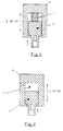
- Fig.1 shows a compression spring type system.
- a compression spring 1 is mounted within the bond head 3 and exerts a force on a movable assembly 2 that connects to a collet bearing the die.
- a die will be held (for example by vacuum) to a collet formed as part of the movable assembly 2.
- the bond head is moved downwardly in the z-direction until the die touches the substrate.
- the bond head 3 continues to move in the z-direction so as to compress the spring 1 against the movable assembly 2 and to exert a bond force on the die through the collet.
- the spring 1 is usually preloaded and the amount of preload directly affects the minimum bond force that can be applied.
- US 5950903 discloses a system similar to the use of a compression spring, but using a leaf spring instead of a compression spring.
- Fig.2 shows a schematic of a prior art example that uses a pneumatic actuator instead of a compression spring.
- a pressure chamber 4 is provided within the bond head housing 6 and acting upon the movable collect assembly 5.
- a variable bond force can be applied by controlling the pressure within the pressure chamber 4.
- a difficulty with this design is that the response time is slow. If the pressure in the chamber 4 is controlled using a pressure regulator the response time is too slow for a real time closed loop control system and instead an open loop control is used instead.
- a related disadvantage is that there is a relatively large impact force. At the moment that the die touches the substrate surface an impact force is produced that acts upon the die.
- an apparatus for providing bond force in a die bonding operation comprising means for generating a primary bond force, means for generating a compensatory bond force, and means for controlling the compensatory bond force whereby a bond force comprising the sum of the primary bond force and the compensatory bond force may be controlled.
- a method of generating a desired bond force in a die bonding operation comprising : providing a primary bond force, generating a compensatory bond force in the same direction or opposite to said primary bond force, summing said primary bond force and said compensatory bond force to generate said bond force, and controlling the magnitude and sign of said compensatory bond force to control said generated bond force.
- a method of controlling the impact force in a die bonding operation comprising moving a bond head bearing a die toward a substrate in a first direction, and providing means for generating a compensatory force in a direction opposite to said first direction at the moment of impact of said die on said substrate.
- a method of preventing vibrations of a collet assembly in a die bond head during translational movement of said bond head comprising generating a force to move said collet assembly against a stop means while said bond head is being moved.
- an important aspect of the present invention is that the apparatus and method involves the provision of a first primary bond force generating means such as a compression spring, and a second compensatory bond force generating means that is capable of rapidly and accurately generating a compensating bond force that may be positive or negative to provide fine control of the primary bond force.
- This compensatory bond force may be generated, for example, by a motor.
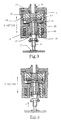
- a bond head according to an embodiment of the invention comprises a bracket 10 for supporting the bond force generating means.
- the primary bond force generating means comprises a compression spring 11 fixed between one end of a shaft 12 and a mount 25 for a bond force motor coil to be described below.
- Compression spring 11 is provided with a preload P and can act upon a collet assembly 14 and die 15 through a slider mount 16.
- a force sensor 17 is located between the slider mount 16 and the collet assembly 14.
- Collet assembly 14 is fixed to slider mount 16 which is formed with bearings 18 that allow the slider mount 16 to slide relative to sliders 19 two of which are formed parallel to the axis of the spring 11, slider mount 16, force sensor 17 and collet assembly 14 (this axis lying on the z-direction). It will thus be understood that the collet assembly 14 may slide relative to the bracket 10 in the z-direction. Collet assembly 14 is adapted to pick and hold a semiconductor die 15 by suction.
- a compensatory bond force generating means is provided in the form of a bond force motor comprising an annular magnet 21 surrounding the spring 11 and sandwiched between a ferromagnetic core 22 and a ferromagnetic plate 23.
- a bond force motor coil 24 is supported on coil mount 25 and is provided in the annular space defined between the edge of the plate 23 and a downwardly extending annular flange portion of the core 22. It will be understood that by the application of a current to the motor coil 24 a force may be generated in the z-direction that acts upon the collet assembly 14.
- this force may be positive (ie downwardly in the z-direction towards the substrate) and will act in addition to the compression spring, or may be negative (ie upwardly in the z-direction away from the substrate) and will act against the compression spring.
- the current applied to the coil 24 may be controlled in response to the output of the force sensor to provide a closed loop control of the bond force.
- the bond head is moved to a location to pick a semiconductor die.
- the die may be held to the collet assembly 14 by vacuum in a conventional manner and is carried to a boding location where the die is to be bonded to a substrate.
- the bond head is then moved downwardly in the z-direction until the die touches the substrate. This point can be detected by the force sensor.
- the first situation (a) may be considered to be described by the equation F ⁇ F mmax + P where F is the required bond force, P is the preload of the compression spring and F mmax is the maximum force generated by the bond force motor.
- the bond force can be controlled solely by varying the output of the bond force motor by varying the current applied to the motor coil.
- a positive force F m may be generated by the bond force motor that acts in addition to the preload P of the spring to provide the required bonding force.
- the force sensor can be used to provide a feedback control of the current supplied to the coil so that the bond motor force is accurately controlled which in turn will accurately control the bond force.
- the required bond force F is smaller than the preload P of the spring, this can be achieved by supplying an opposite current to the bond force motor coil so that the bond force motor generates a negative force that acts upwardly against the compression spring. Again this negative bond motor force can be accurately controlled by a closed loop control using the force sensor.
- Situation (b) may be considered to be represented by the equation F ⁇ F mmax + P.
- the required bond force is obtained by controlling the force F m of the bond force motor and the force F s generated by the spring.
- the force generated by the bond force motor is controlled by supplying a current to the motor coil as discussed above.
- the force generated by the spring is controlled by moving the bond head further downwardly towards the substrate surface.
- the collet assembly and die cannot move any further, and therefore there is a relative movement z of the collet assembly and die in the direction of the arrow A in Fig. 4 that serves to compress the spring by a distance z and the force generated by the spring will increase to P + kz where k is the spring constant of the spring.
- the total bond force is F m + P + kz and this can be controlled rapidly and accurately by varying the current to the motor coil to change F m in response to closed loop control from the force sensor.
- a primary bond force generating means in the form of the compression spring (though this could be replaced by a leaf spring or by a pneumatic actuator).
- a compensatory bond force generating means in the form of a bond force motor.
- the compression spring provides the main element of the bond force with all the advantages of a compression spring (simple construction, large available range of bond force), but the addition of a positive or negative compensatory bond force from the bond force motor allows the total bond force to be rapidly and accurately controlled by means of a closed loop control of the current supplied to the motor coil.
- a further advantage of the present invention is that it allows the impact force to be minimized. This can be achieved by allowing the bond force motor to generate a negative bond force at the moment of impact and before the bonding process is commenced.
- another advantage is that vibration of the bond head during movement can be reduced using the embodiment of the invention.
- vibrations of the collet assembly within the bond head can be reduced by using the bond force motor to generate a negative bond force that causes the collet assembly to move upwardly relative to the remainder of the bond head as far as it can until it reaches a stop position.
Landscapes
- Engineering & Computer Science (AREA)
- Mechanical Engineering (AREA)
- Die Bonding (AREA)
- Manipulator (AREA)
Applications Claiming Priority (2)
| Application Number | Priority Date | Filing Date | Title |
|---|---|---|---|
| US905906 | 1986-09-10 | ||
| US09/905,906 US6616031B2 (en) | 2001-07-17 | 2001-07-17 | Apparatus and method for bond force control |
Publications (3)
| Publication Number | Publication Date |
|---|---|
| EP1278232A2 true EP1278232A2 (de) | 2003-01-22 |
| EP1278232A3 EP1278232A3 (de) | 2003-05-02 |
| EP1278232B1 EP1278232B1 (de) | 2004-11-10 |
Family
ID=25421668
Family Applications (1)
| Application Number | Title | Priority Date | Filing Date |
|---|---|---|---|
| EP02254979A Expired - Lifetime EP1278232B1 (de) | 2001-07-17 | 2002-07-16 | Apparat und Methode zur Kontrolle der Verbindungskraft |
Country Status (4)
| Country | Link |
|---|---|
| US (1) | US6616031B2 (de) |
| EP (1) | EP1278232B1 (de) |
| CN (1) | CN1179405C (de) |
| SG (1) | SG99406A1 (de) |
Cited By (2)
| Publication number | Priority date | Publication date | Assignee | Title |
|---|---|---|---|---|
| DE102005057648B4 (de) * | 2004-12-06 | 2008-07-10 | Oerlikon Assembly Equipment Ag, Steinhausen | Verfahren für die Montage eines Halbleiterchips auf einem Substrat |
| US8262146B2 (en) | 2006-12-11 | 2012-09-11 | Robert Bosch Gmbh | Handling tools for components, in particular eletronic components |
Families Citing this family (30)
| Publication number | Priority date | Publication date | Assignee | Title |
|---|---|---|---|---|
| US7441688B2 (en) * | 2003-11-04 | 2008-10-28 | Reactive Nanotechnologies | Methods and device for controlling pressure in reactive multilayer joining and resulting product |
| TW510507U (en) * | 2002-04-22 | 2002-11-11 | Ind Tech Res Inst | Chip accessing device with position, speed and force controls |
| TW200414992A (en) * | 2002-11-29 | 2004-08-16 | Esec Trading Sa | Method for picking semiconductor chips from a foil |
| EP1424884A1 (de) * | 2002-11-29 | 2004-06-02 | Leica Geosystems AG | Verfahren zur Montage miniaturisierter Bauteile auf einer Trägerplatte |
| JP4166620B2 (ja) * | 2003-05-13 | 2008-10-15 | オリンパス株式会社 | 半導体接合装置 |
| JP4616748B2 (ja) * | 2005-10-11 | 2011-01-19 | 株式会社新川 | ダイピックアップ装置 |
| DE102006020418A1 (de) * | 2006-04-26 | 2007-10-31 | Herrmann Ultraschalltechnik Gmbh & Co. Kg | Vorrichtung zum Bearbeiten von Werkstücken mittels Ultraschall |
| CH698844B1 (de) * | 2007-06-22 | 2009-11-13 | Oerlikon Assembly Equipment Ag | Vorrichtung zum Anpressen von auf einem Substrat angeordneten Halbleiterchips. |
| TWI377902B (en) * | 2009-10-19 | 2012-11-21 | Wistron Corp | Pressing device for heat sink and pressing tool of the pressing device |
| JP2013026268A (ja) * | 2011-07-15 | 2013-02-04 | Hitachi High-Tech Instruments Co Ltd | 2軸駆動機構及びダイボンダ |
| US9034199B2 (en) | 2012-02-21 | 2015-05-19 | Applied Materials, Inc. | Ceramic article with reduced surface defect density and process for producing a ceramic article |
| US9212099B2 (en) | 2012-02-22 | 2015-12-15 | Applied Materials, Inc. | Heat treated ceramic substrate having ceramic coating and heat treatment for coated ceramics |
| US9090046B2 (en) | 2012-04-16 | 2015-07-28 | Applied Materials, Inc. | Ceramic coated article and process for applying ceramic coating |
| US10199350B2 (en) * | 2012-05-25 | 2019-02-05 | Asm Technology Singapore Pte Ltd | Apparatus for heating a substrate during die bonding |
| US9604249B2 (en) | 2012-07-26 | 2017-03-28 | Applied Materials, Inc. | Innovative top-coat approach for advanced device on-wafer particle performance |
| US9343289B2 (en) | 2012-07-27 | 2016-05-17 | Applied Materials, Inc. | Chemistry compatible coating material for advanced device on-wafer particle performance |
| US9916998B2 (en) | 2012-12-04 | 2018-03-13 | Applied Materials, Inc. | Substrate support assembly having a plasma resistant protective layer |
| US9685356B2 (en) | 2012-12-11 | 2017-06-20 | Applied Materials, Inc. | Substrate support assembly having metal bonded protective layer |
| US8941969B2 (en) | 2012-12-21 | 2015-01-27 | Applied Materials, Inc. | Single-body electrostatic chuck |
| US9358702B2 (en) | 2013-01-18 | 2016-06-07 | Applied Materials, Inc. | Temperature management of aluminium nitride electrostatic chuck |
| US9669653B2 (en) | 2013-03-14 | 2017-06-06 | Applied Materials, Inc. | Electrostatic chuck refurbishment |
| US9887121B2 (en) | 2013-04-26 | 2018-02-06 | Applied Materials, Inc. | Protective cover for electrostatic chuck |
| US9666466B2 (en) | 2013-05-07 | 2017-05-30 | Applied Materials, Inc. | Electrostatic chuck having thermally isolated zones with minimal crosstalk |
| US9865434B2 (en) | 2013-06-05 | 2018-01-09 | Applied Materials, Inc. | Rare-earth oxide based erosion resistant coatings for semiconductor application |
| US9850568B2 (en) | 2013-06-20 | 2017-12-26 | Applied Materials, Inc. | Plasma erosion resistant rare-earth oxide based thin film coatings |
| CN104517876B (zh) * | 2013-09-30 | 2018-11-27 | 韩华泰科株式会社 | 封装件运送器组件 |
| US10020218B2 (en) | 2015-11-17 | 2018-07-10 | Applied Materials, Inc. | Substrate support assembly with deposited surface features |
| US11047035B2 (en) | 2018-02-23 | 2021-06-29 | Applied Materials, Inc. | Protective yttria coating for semiconductor equipment parts |
| CN120674328A (zh) * | 2025-03-14 | 2025-09-19 | 智慧星空(上海)工程技术有限公司 | 键合头、键合装置、键合方法及存储介质 |
| CN121772695A (zh) * | 2026-03-04 | 2026-03-31 | 智慧星空(上海)工程技术有限公司 | 基片贴装头及半导体设备 |
Family Cites Families (23)
| Publication number | Priority date | Publication date | Assignee | Title |
|---|---|---|---|---|
| US3727822A (en) | 1970-10-05 | 1973-04-17 | Gen Electric | Electromagnetic force system for integrated circuit fabrication |
| US3940047A (en) * | 1974-01-16 | 1976-02-24 | Unitek Corporation | Bonding apparatus utilizing pivotally mounted bonding arm |
| US4266710A (en) * | 1978-11-22 | 1981-05-12 | Kulicke And Soffa Industries Inc. | Wire bonding apparatus |
| US4597522A (en) * | 1983-12-26 | 1986-07-01 | Kabushiki Kaisha Toshiba | Wire bonding method and device |
| US4603802A (en) | 1984-02-27 | 1986-08-05 | Fairchild Camera & Instrument Corporation | Variation and control of bond force |
| US4850780A (en) * | 1987-09-28 | 1989-07-25 | Kulicke And Soffa Industries Inc. | Pre-peel die ejector apparatus |
| JPH04162730A (ja) | 1990-10-26 | 1992-06-08 | Nec Kyushu Ltd | ダイボンディング装置の押圧力制御機構 |
| US5138127A (en) * | 1991-07-31 | 1992-08-11 | Hughes Aircraft Company | Pressure welding with closed loop force control |
| US5285946A (en) * | 1991-10-11 | 1994-02-15 | Sanyo Electric Co., Ltd. | Apparatus for mounting components |
| US5230458A (en) * | 1992-06-23 | 1993-07-27 | National Semiconductor Corp. | Interconnect formation utilizing real-time feedback |
| JP2635889B2 (ja) * | 1992-06-24 | 1997-07-30 | 株式会社東芝 | ダイボンディング装置 |
| US5240165A (en) * | 1992-07-06 | 1993-08-31 | Motorola, Inc. | Method and apparatus for controlled deformation bonding |
| US5368217A (en) * | 1993-08-25 | 1994-11-29 | Microelectronics And Computer Technology Corporation | High force compression flip chip bonding method and system |
| US5586713A (en) * | 1993-08-31 | 1996-12-24 | Matsushita Electric Industrial Co., Ltd. | Method for wire bonding |
| US5608172A (en) | 1995-03-16 | 1997-03-04 | Texas Instruments Incorporated | Die bond touch down detector |
| US5673844A (en) * | 1995-12-29 | 1997-10-07 | Gte Laboratories Incorporated | Gas pressure adjustable diebonding apparatus and method |
| US5985064A (en) * | 1996-11-28 | 1999-11-16 | Matsushita Electric Industrial Co., Ltd. | Chip compression-bonding apparatus and method |
| EP0864392B1 (de) | 1997-03-13 | 2001-08-16 | F & K Delvotec Bondtechnik GmbH | Bondkopf |
| JP3370551B2 (ja) * | 1997-04-02 | 2003-01-27 | 株式会社新川 | ワイヤボンディング装置及びそのボンディング荷重補正方法 |
| EP1187180A1 (de) * | 2000-09-12 | 2002-03-13 | Esec Trading S.A. | Verfahren und Vorrichtung für die Montage von Halbleiterchips |
| KR100773170B1 (ko) * | 2000-09-12 | 2007-11-02 | 언액시스 인터내셔널 트레이딩 엘티디 | 반도체 칩을 장착하는 방법 및 장치 |
| JP4538942B2 (ja) * | 2000-10-30 | 2010-09-08 | 日本電気株式会社 | ワイヤボンディング装置 |
| JP4544755B2 (ja) * | 2001-01-17 | 2010-09-15 | パナソニック株式会社 | ボンディングヘッド及び部品装着装置 |
-
2001
- 2001-07-17 US US09/905,906 patent/US6616031B2/en not_active Expired - Lifetime
-
2002
- 2002-07-16 EP EP02254979A patent/EP1278232B1/de not_active Expired - Lifetime
- 2002-07-17 CN CNB021263361A patent/CN1179405C/zh not_active Expired - Lifetime
- 2002-07-17 SG SG200204361A patent/SG99406A1/en unknown
Cited By (3)
| Publication number | Priority date | Publication date | Assignee | Title |
|---|---|---|---|---|
| DE102005057648B4 (de) * | 2004-12-06 | 2008-07-10 | Oerlikon Assembly Equipment Ag, Steinhausen | Verfahren für die Montage eines Halbleiterchips auf einem Substrat |
| US7407084B2 (en) | 2004-12-06 | 2008-08-05 | Unaxis Trading Ltd | Method for mounting a semiconductor chip onto a substrate |
| US8262146B2 (en) | 2006-12-11 | 2012-09-11 | Robert Bosch Gmbh | Handling tools for components, in particular eletronic components |
Also Published As
| Publication number | Publication date |
|---|---|
| US6616031B2 (en) | 2003-09-09 |
| SG99406A1 (en) | 2003-10-27 |
| US20030015569A1 (en) | 2003-01-23 |
| CN1399320A (zh) | 2003-02-26 |
| EP1278232A3 (de) | 2003-05-02 |
| CN1179405C (zh) | 2004-12-08 |
| EP1278232B1 (de) | 2004-11-10 |
Similar Documents
| Publication | Publication Date | Title |
|---|---|---|
| EP1278232B1 (de) | Apparat und Methode zur Kontrolle der Verbindungskraft | |
| Qin et al. | A novel direct inverse modeling approach for hysteresis compensation of piezoelectric actuator in feedforward applications | |
| Futami et al. | Nanometer positioning and its micro-dynamics | |
| Delibas et al. | A method to realize low velocity movability and eliminate friction induced noise in piezoelectric ultrasonic motors | |
| KR101842624B1 (ko) | 전자부품의 실장 장치 | |
| US20030156270A1 (en) | Multiple degree of freedom substrate manipulator | |
| US6899262B2 (en) | Clamping device | |
| EP0297574A2 (de) | Antriebsanordnung, die mittels piezoelektrischer Elemente einen angetriebenen Teil antreibt | |
| CN100482408C (zh) | 姿势控制器和精密加工设备 | |
| JP3961162B2 (ja) | 電子部品装着装置および電子部品装着方法 | |
| JP3135404B2 (ja) | ステージ装置とこれを用いたシステム | |
| JP4515508B2 (ja) | ワーク実装装置 | |
| CN120527246A (zh) | 晶圆键合压力控制机构及方法 | |
| JP3856375B2 (ja) | 実装装置およびその制御方法 | |
| JP4051881B2 (ja) | 制動機構および電子顕微鏡用試料ステージ | |
| JP2002043797A (ja) | 電子部品実装装置 | |
| JP3700135B2 (ja) | ボンディング装置 | |
| WO2009136504A1 (ja) | 精密位置決め装置 | |
| Jie et al. | Design and simulation of a macro-micro dual-drive high acceleration precision XY-stage for IC bonding technology | |
| Lin et al. | A novel high precision electromagnetic flexure-suspended positioning stage with an eddy current damper | |
| JP2001242937A (ja) | ステージ装置 | |
| JP2006114559A (ja) | 電子部品接合装置 | |
| JP2006114560A (ja) | 電子部品接合装置 | |
| JP2004531076A (ja) | 対象物を基板に載着するための載着装置および方法 | |
| JPS614634A (ja) | リニアモ−タ駆動形浮上式ステ−ジの弾性送り位置決め機構 |
Legal Events
| Date | Code | Title | Description |
|---|---|---|---|
| PUAI | Public reference made under article 153(3) epc to a published international application that has entered the european phase |
Free format text: ORIGINAL CODE: 0009012 |
|
| 17P | Request for examination filed |
Effective date: 20021004 |
|
| AK | Designated contracting states |
Kind code of ref document: A2 Designated state(s): AT BE BG CH CY CZ DE DK EE ES FI FR GB GR IE IT LI LU MC NL PT SE SK TR |
|
| AX | Request for extension of the european patent |
Free format text: AL;LT;LV;MK;RO;SI |
|
| RIC1 | Information provided on ipc code assigned before grant |
Ipc: 7H 01L 21/00 A Ipc: 7B 23K 20/00 B |
|
| PUAL | Search report despatched |
Free format text: ORIGINAL CODE: 0009013 |
|
| AK | Designated contracting states |
Designated state(s): AT BE BG CH CY CZ DE DK EE ES FI FR GB GR IE IT LI LU MC NL PT SE SK TR |
|
| AX | Request for extension of the european patent |
Extension state: AL LT LV MK RO SI |
|
| 17Q | First examination report despatched |
Effective date: 20030328 |
|
| AKX | Designation fees paid |
Designated state(s): CH LI NL |
|
| REG | Reference to a national code |
Ref country code: DE Ref legal event code: 8566 |
|
| GRAP | Despatch of communication of intention to grant a patent |
Free format text: ORIGINAL CODE: EPIDOSNIGR1 |
|
| GRAS | Grant fee paid |
Free format text: ORIGINAL CODE: EPIDOSNIGR3 |
|
| GRAA | (expected) grant |
Free format text: ORIGINAL CODE: 0009210 |
|
| AK | Designated contracting states |
Kind code of ref document: B1 Designated state(s): CH LI NL |
|
| REG | Reference to a national code |
Ref country code: CH Ref legal event code: EP |
|
| REG | Reference to a national code |
Ref country code: CH Ref legal event code: NV Representative=s name: A. BRAUN, BRAUN, HERITIER, ESCHMANN AG PATENTANWAE |
|
| PLBE | No opposition filed within time limit |
Free format text: ORIGINAL CODE: 0009261 |
|
| STAA | Information on the status of an ep patent application or granted ep patent |
Free format text: STATUS: NO OPPOSITION FILED WITHIN TIME LIMIT |
|
| 26N | No opposition filed |
Effective date: 20050811 |
|
| REG | Reference to a national code |
Ref country code: CH Ref legal event code: PFA Owner name: ASM ASSEMBLY AUTOMATION LTD. Free format text: ASM ASSEMBLY AUTOMATION LTD.#20/F., WATSON CENTRE, 16-22 KUNG YIP STREET#KWAI CHUNG, HONG KONG (CN) -TRANSFER TO- ASM ASSEMBLY AUTOMATION LTD.#20/F., WATSON CENTRE, 16-22 KUNG YIP STREET#KWAI CHUNG, HONG KONG (CN) |
|
| REG | Reference to a national code |
Ref country code: CH Ref legal event code: PCAR Free format text: NEW ADDRESS: HOLBEINSTRASSE 36-38, 4051 BASEL (CH) |
|
| PGFP | Annual fee paid to national office [announced via postgrant information from national office to epo] |
Ref country code: NL Payment date: 20210716 Year of fee payment: 20 |
|
| PGFP | Annual fee paid to national office [announced via postgrant information from national office to epo] |
Ref country code: CH Payment date: 20210715 Year of fee payment: 20 |
|
| REG | Reference to a national code |
Ref country code: NL Ref legal event code: MK Effective date: 20220715 |
|
| REG | Reference to a national code |
Ref country code: CH Ref legal event code: PL |