EP1279005B1 - Unite de balayage pour dispositif de mesure optique de la position - Google Patents
Unite de balayage pour dispositif de mesure optique de la position Download PDFInfo
- Publication number
- EP1279005B1 EP1279005B1 EP01931606A EP01931606A EP1279005B1 EP 1279005 B1 EP1279005 B1 EP 1279005B1 EP 01931606 A EP01931606 A EP 01931606A EP 01931606 A EP01931606 A EP 01931606A EP 1279005 B1 EP1279005 B1 EP 1279005B1
- Authority
- EP
- European Patent Office
- Prior art keywords
- detector
- scanning
- scanning unit
- detector elements
- arrays
- Prior art date
- Legal status (The legal status is an assumption and is not a legal conclusion. Google has not performed a legal analysis and makes no representation as to the accuracy of the status listed.)
- Expired - Lifetime
Links
- 230000003287 optical effect Effects 0.000 title claims description 11
- 238000003491 array Methods 0.000 claims description 55
- 238000001514 detection method Methods 0.000 claims description 19
- 230000000737 periodic effect Effects 0.000 claims description 11
- 230000005855 radiation Effects 0.000 claims description 5
- 239000000758 substrate Substances 0.000 claims description 2
- 230000010363 phase shift Effects 0.000 claims 1
- 238000005259 measurement Methods 0.000 description 11
- 238000005070 sampling Methods 0.000 description 8
- 230000005540 biological transmission Effects 0.000 description 4
- 238000011109 contamination Methods 0.000 description 2
- 238000005191 phase separation Methods 0.000 description 2
- 230000015572 biosynthetic process Effects 0.000 description 1
- 230000001419 dependent effect Effects 0.000 description 1
- 230000000694 effects Effects 0.000 description 1
- 230000010354 integration Effects 0.000 description 1
- 238000004519 manufacturing process Methods 0.000 description 1
- 239000003550 marker Substances 0.000 description 1
Images

Classifications
-
- G—PHYSICS
- G01—MEASURING; TESTING
- G01D—MEASURING NOT SPECIALLY ADAPTED FOR A SPECIFIC VARIABLE; ARRANGEMENTS FOR MEASURING TWO OR MORE VARIABLES NOT COVERED IN A SINGLE OTHER SUBCLASS; TARIFF METERING APPARATUS; MEASURING OR TESTING NOT OTHERWISE PROVIDED FOR
- G01D5/00—Mechanical means for transferring the output of a sensing member; Means for converting the output of a sensing member to another variable where the form or nature of the sensing member does not constrain the means for converting; Transducers not specially adapted for a specific variable
- G01D5/26—Mechanical means for transferring the output of a sensing member; Means for converting the output of a sensing member to another variable where the form or nature of the sensing member does not constrain the means for converting; Transducers not specially adapted for a specific variable characterised by optical transfer means, i.e. using infrared, visible, or ultraviolet light
- G01D5/32—Mechanical means for transferring the output of a sensing member; Means for converting the output of a sensing member to another variable where the form or nature of the sensing member does not constrain the means for converting; Transducers not specially adapted for a specific variable characterised by optical transfer means, i.e. using infrared, visible, or ultraviolet light with attenuation or whole or partial obturation of beams of light
- G01D5/34—Mechanical means for transferring the output of a sensing member; Means for converting the output of a sensing member to another variable where the form or nature of the sensing member does not constrain the means for converting; Transducers not specially adapted for a specific variable characterised by optical transfer means, i.e. using infrared, visible, or ultraviolet light with attenuation or whole or partial obturation of beams of light the beams of light being detected by photocells
- G01D5/36—Forming the light into pulses
- G01D5/366—Particular pulse shapes
Definitions
- the present invention relates to a scanning unit for an optical position measuring device according to the preamble of claim 1.
- Known optical position-measuring devices usually include a Scale with a measuring graduation and a relatively movable Scanning unit.
- a detection plane of the scanning unit results in the case the relative movement is a periodic modulation of a stripe pattern
- the via a suitable arrangement of electro-optical detector elements for generating detected by incremental signals and to determine the relative position is evaluated by scale and scanning unit.
- the phase offset is usually 90 °.
- reference pulse signal from the scanning of a reference mark generated and with the information relative to the relative position, i. with the incremental signals charged.
- a generic scanning unit is, for example, from FIG. 3a of WO 99/08074 known.
- the scanning unit proposed therein is in this case in particular suitable for scanning an incremental measuring graduation, in the One or more positions directly integrated a reference mark is.
- the scanning unit comprises for scanning the periodic stripe pattern in the detection plane, a detector arrangement with a detector array with several radiation sensitive detector elements, which in a first direction are arranged adjacent to each other.
- the first Direction corresponds to the measuring direction x along which the measurement graduation and the scanning unit are arranged to be movable relative to each other.
- DE-36 16 144 A discloses a scanning unit for a position measuring device, with several Detector arrays as defined in the preambles of claims 1 and 13, wherein the Detector arrays are arranged so that the harmonic components targeted from the output signal can be eliminated.
- Object of the present invention is therefore to provide a scanning unit for a specify optical position measuring device, the incremental in the generation Sampling signals also due to possible short-period disturbances the sampled measurement division is disturbed as little as possible.
- the scanning unit according to the invention now ensures that as well possible short-period disturbances in the sampled measuring graduation the Generation of periodic incremental signals and their further processing affect less faulty.
- Design of the scanning unit a so-called one-field scanning ensuring that the different out of phase, incremental samples from a single period of the sampled Stripe pattern to be won. Also in case of a possible short-periodic Disturbance results in a uniform influence on all signals.
- the scanning unit according to the invention is particularly suitable for position-measuring devices which have an integrated into the measuring graduation Have reference mark.
- the present invention but also be used in systems that do not produce such provide a reference pulse signal.
- the present invention also proves in the case of larger contamination of the measurement division as advantageous and provides this the largely uniform influence on all phase-shifted scanning signals for sure.
- the present invention can of course be used in both incident and as well as in transmitted-light systems; Likewise, linear and Rotational position measuring devices are designed accordingly.
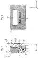
- FIG. 1 shows the scanning beam path of a first optical position-measuring device illustrated in which a first variant of the invention Scanning unit is used.
- the first example shown in FIG Incident position measuring device comprises a scale 2 and a relative to the scale 2 in the measuring direction x movable scanning unit 1.
- the measuring direction x is oriented perpendicular to the plane of the drawing.
- a known incremental measuring graduation 20 On the scale 2 side is a known incremental measuring graduation 20 provided, which extends in the measuring direction x and from a periodic Sequence of reflective and non-reflective sub-areas consists.
- a reference mark integrated At one or more defined points in the measurement graduation is a reference mark integrated, as in the already mentioned WO 99/08074 is about the scanning of the reference mark and the generation of a reference pulse signal REF can be during the position measurement manufacture the absolute cover in a known manner.
- the scanning unit 1 has a detector arrangement 6, which at the scale 2 facing bottom of the Board 3 is arranged.
- the detector arrangement 6 reference is made to the following description of Figure 3.
- a scanning plate 7 is provided on the side of the scanning unit 1, a transmission structure 71 and a transparent window area 72nd having.
- a plan view of the scanning 7 is shown in Figure 2.
- the beams S emitted by the light source 4 arrive first on the collimator optics 5 and are deflected by this and at the same time teilkollimiert. Subsequently, the radiation beams pass through an opening 31 in the board 3 and then go through the transmission structure 71 in the Abtastsplatte 7, before they hit the graduation 20 on the scale 2. From there, a return reflection of the beam in the direction of scanning takes place 1. In the scanning unit 1, the beams pass through the transparent Window portion 72 in the scanning 7, which no further optical Effect before finally resulting in the detection level, periodic fringe pattern is detected via the detector array 6. about the scanning beam path shown results in the detection plane of Scanning unit a stripe pattern with a variety of narrow stripes.
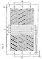
- FIG. 3 shows the overall view of the in the example of Figure 1 used detector assembly. 6
- the scanning signals in this case have a relative phase offset of 90 ° to each other; in the following, in this context, the scanning signals S0, S90, S180, S270 the speech.
- each detector element D assigned number gives the relative phase of the Abtastsignales S0, S90, S180, S270 connected to the respective detector element D in the Scanning the periodic stripe pattern generated in the detection plane becomes.
- each individual detector array thus provides A1-A6 already have the required four phase-shifted scanning signals S0, S90, S180, S270.
- the in-phase detector elements D each individual detector array A1 - A6 electrically conductively connected to each other.
- the connection lines in Fig. 3rd not shown. In connection with an advantageous variant regarding. Let the connection of the different in-phase detector elements D be to the corresponding application of the applicant with the same exam day directed.
- the illustrated embodiment of a detector arrangement 6 of the scanning unit according to the invention in addition to the detector arrays A1 - A6 for generating one or more reference pulse signals REF comprises a total of six reference pulse detector elements R1 - R6.
- a reference marker integrated in the incremental measuring graduation can be scanned via the reference pulse detector elements R1-R6.
- the reference pulse detector elements R1 - R6 are placed in the center of the detector array 6.
- a first group G1 with the three detector arrays A1-A3 is arranged to the left of the reference pulse detector elements R1-R6;
- the second group G2 with the three detector arrays A4-A6 is arranged on the right next to the reference pulse detector elements R1-R6.
- every second one of the reference pulse detector elements R1-R6 is connected to one another in an electrically conductive manner.
- a so-called reference pulse clock signal RI T is generated in this case via a first group of reference pulse detector elements R1, R3 and R5 connected in this way; the second group with the associated reference pulse detector elements R2, R4 and R6 supplies a so-called reference pulse push-pull signal RI GT .
- reference pulse push-pull signal RI GT With regard to the processing of the signals RI T and RI GT for the finally resulting reference pulse signal REF, reference is made at this point only to WO 99/08074.
- detector arrays A1 - A6 each consist of several radiation-sensitive detector elements D. All detector arrays A1-A6 have the same number of detector elements D in this example.
- the detector elements D are each adjacent in a first direction x arranged on a common carrier substrate 60 to each other.
- the first direction x is identical to the measuring direction mentioned in FIG x.
- Per detector array A1 - A6 are in one possible embodiment about 60 detector elements D used. In Figure 3 are off For clarity, only a smaller number of Detector elements D per detector array A1 - A6 shown.
- the six detector arrays A1 - A6 all have the basically identical structure in the example shown; decisive for the present invention is its relative arrangement, which will be discussed in detail later.
- the detector arrays A1-A6 each comprise a multiplicity of rectangular detector elements D which have the width b in the first direction x and the length l perpendicularly thereto in the second direction y.
- the detector elements D are furthermore arranged periodically in all six detector arrays A1-A6 in the first direction x with the detector period P DET .
- the periodic fringe pattern resulting in the detection plane is sampled, which has the fine fringe pattern period P SM in this example.
- a plurality of detector arrays A1 - A3 and A4 - A6 are arranged adjacent to each other at a distance D y .
- Each of the Detektorarryas A1 - A6 basically provides the four required phase-shifted scanning signals; the provision of a plurality of detector arrays A1-A6 in the manner illustrated ultimately ensures the desired single-field scanning, in which all phase-shifted scanning signals S0, S90, S180, S270 result from a sampled period P SM of the fringe pattern. Even in the event of a possible short-period disturbance, there is then a uniform influencing of all scanning signals S0, S90, S180, S270 within a fringe pattern period P SM.
- the detector elements D of the further detector arrays A2, A5 or A3, A6 are arranged offset in the first direction x relative to the detector elements D of the first detector array A1 or A4 by a certain amount.
- S180, S270 can be generated.
- FIG. 4 a further embodiment of a detector assembly 6 'in one schematic sectional view shows.
- the phase position 0 ° for the scanning signal S0 generated via the first detector element D therefore results in the first detector array A1 '.
- the right in the measuring direction x adjacent detector element D delivers at the specified sizes P SM , b and d incremental scanning S270 with the relative phase 270 °.
- the scanning signals S180, S90 with the relative phase positions 180 °, 90 °, before in turn a detector element D follows, the scanning signals S0 generated with the relative phase position 0 ° etc ..
- the same sequence of the scanning signals S0, S270, S180, S90 generated via the detector elements D is also provided in the two other further required detector arrays A2 'and A3', which are arranged in the y-direction adjacent to the first detector array A1 '.
- the respective distance of adjacent detector arrays A1 ', A2', A3 ' is denoted by D y .
- the results Phase separation or the generation of the desired phase-shifted Scanning signals from the explained arrangement of the various detector elements D.
- every detector array A1 - A6 delivers already all four desired phase-shifted scanning signals S0 - S270; the described juxtaposition of several detector arrays in y-direction also faces the desired insensitivity short period disturbances.
- the illustrated arrangement of the three detector arrays A1 '- A3' of basically not of relevance, i.e. it could be self-evident also another sequence of the three detector arrays A1 '- A3' in the y direction be provided.
- Essential for the desired effect is only their relative arrangement to each other in the first direction x, i. of the corresponding respective relative offset in the measuring direction x.
- other predetermined quantities may also require a different number k of adjacent detector arrays.
- the corresponding phase offset ⁇ 1i can be determined from the required geometric offset ⁇ x 1i .
- the opposite of the position measuring device Figure 1 has a slightly modified scanning beam. So includes the corresponding position measuring device in contrast to first example in Figure 1 in the transparent window portion 72 of the scanning 7 is a scanning structure.
- a plan view of the associated scanning this position measuring device is in Figure 5 shown.
- the scanning plate 17 again comprises a transmission structure 171; in the adjacent area is however additionally provided a scanning structure 172.
- the scanning structure 172 consists in this example of four separate Abtastfeldem for Generation of the incremental scanning signals.
- the scanning fields in the y direction are arranged adjacent to each other, here have a specific Offset to each other. In the middle area is that part of the Scanning structure 172 can be seen, which is used to generate the reference pulse signal serves.
- the beams of rays reflected by the measuring graduation thus pass through the scanning structure 172 in the scanning plate 17 before impinging on the detector plane.
- This scanning beam path results in a significantly coarser fringe pattern in the detection plane, ie a significantly larger fringe pattern period P SM . as resulted in the first example.
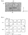
- Each of the separate scanning fields is assigned a detector array in the detection plane. This in turn results in a slightly modified design of the detector arrangement, which will now be explained with reference to FIG.
- Detector arrays A1 ", A2" adjacent in the y direction have the spacing D y .
- Each individual detector array A1 ", A2" generates as in the previous example already explains the basically required four phase-shifted Sampling signals S0 - S270.
- the adjacent arrangement of several detector arrays A1 ", A2" again serves only for the desired compensation short periodic error in the measurement graduation.
- only the most important short-period errors compensated because within the graduation period of the sampled graduation, respectively only the antiphase or 180 ° out of phase scanning signals S0 and S180 or S90 and S270 are generated. This affects the mentioned short-term disturbances ultimately equally on the offset components of the antiphase scanning signals, so that the further processed Difference signal from these scanning signals even with such interference has no distorting offset component.
- the individual detector elements D of the successive detector arrays A1 "and A2" in the y-direction are arranged without geometric relative offset to one another in the x-direction, ie in the y-direction, the delector elements D are in principle arranged exactly in alignment.
- the detector elements of different detector arrays A1 "and A2" arranged directly beneath one another detect in this system not in-phase scanning signals; Rather, those detector elements which detect phase-identical scanning signals are arranged offset in the measuring direction x in the various detector arrays A1 ", A2".
- the detector elements in the first and second detector array A1 "or A2" which respectively detect in phase scanning signals are offset by the amount ⁇ x 12 in positive x-direction relative to one another.
- Detector elements D in this scanning principle also result from the partial regions of the scanning structure 172 offset from one another in the measuring direction x, as is indicated schematically in FIG.
- the phase separation is carried out in this optical position measuring device accordingly the correspondingly formed scanning structure 172 in the scanning 17 in conjunction with the offset amount ⁇ x 12 of the detector elements D.
- this variant can also be formed with n detector arrays arranged one above the other in order to generate the desired n phase-shifted scanning signals.
- all n phase-shifted scanning signals are generated via the n aligned detector elements D arranged.
- the partial regions of the scanning structure assigned to the detector arrays are to be arranged offset in such a way that in the detection plane the associated fringe patterns have an offset of m i * P SM / n.
- division structures may be used instead of the scanning structure divided in the scanning beam in several staggered sections are then in turn associated with corresponding detector arrays become; for example, a transmission sharing structure could accordingly also be used or a measuring graduation can be divided in such a way etc ..
Landscapes
- Physics & Mathematics (AREA)
- General Physics & Mathematics (AREA)
- Optical Transform (AREA)
- Length Measuring Devices By Optical Means (AREA)
Claims (12)
- Unité de balayage pour un dispositif de mesure optique de position pour le palpage d'un motif de bandes périodique dans un plan de détection, composé d'un système de détecteurs, qui comprend au moins une rangée de détecteurs avec plusieurs détecteurs élémentaires sensibles au rayonnement, qui sont disposés les uns à côté des autres dans une première direction sur un substrat support,caractérisée par le fait qu'à l'intérieur de chaque rangée de détecteurs (A1-A6), les détecteurs élémentaires (D) sont disposés périodiquement avec des espaces (PDET) équidistants, dans chaque rangée de détecteurs (A1-A6) n détecteurs élémentaires (D) disposés l'un derrière l'autre délivrant les n signaux de palpage déphasés nécessaires.au moins une deuxième rangée de détecteurs avec plusieurs détecteurs élémentaires sensibles au rayonnement, étant disposée à côté de la première rangée de détecteurs, dans une deuxième direction perpendiculaire à la première direction, dans le plan de détection,les détecteurs élémentaires de la deuxième rangée de détecteurs étant disposés également les uns à côté des autres dans la première direction etles détecteurs élémentaires de la deuxième rangée de détecteurs présentant un décalage géométrique défini dans la première direction par rapport aux détecteurs élémentaires de la première rangée de détecteurs,
- Unité de balayage selon la revendication 1, caractérisée par le fait qu'il est prévu au total k rangées de détecteurs (A1, A2, A3 ; A4, A5, A6) et que le décalage (Δx1i) des détecteurs élémentaires (D) des différentes rangées de détecteurs (A1, A2, A3 ; A4, A5, A6) est choisi de telle sorte qu'il résulte du palpage d'une période PSM du motif de bandes, n signaux de palpage avec un déphasage relatif de 360°/n délivrés par les détecteurs élémentaires (D) des k rangées de détecteurs (A1, A2, A3 ; A4, A5, A6).
- Unité de balayage selon la revendication 2, caractérisée par le fait que le nombre (k) de rangées de détecteurs nécessaires est donné par
avec n = 2, 3, 4 ... et PDET : période de détecteur. - Unité de balayage selon la revendication 3, caractérisée par le fait que le décalage géométrique Δx1i de la i-ème rangée de détecteurs A, parmi au total k rangées de détecteurs nécessaires, par rapport à une première rangée de détecteurs A1 dans la direction de mesure x est
- Unité de balayage selon la revendication 3, caractérisée par le fait qu'on choisit k = 3 et n = 4.
- Unité de balayage selon la revendication 2, caractérisée par le fait que les détecteurs élémentaires (D) de toutes les rangées de détecteurs (A1, A2, A3 ; A4, A5, A6) sont conformées chaque fois en rectangles, dont la largeur b est orientée dans la première direction (x) et la longueur 1 dans la deuxième direction (y).
- Unité de balayage selon la revendication 6, caractérisée par le fait que les détecteurs élémentaires (D) de rangées de détecteurs (A1, A2, A3 ; A4, A5, A6) voisines sont espacés d'une distance Dy..
- Unité de balayage selon la revendication 2, caractérisée par le fait qu'à l'intérieur de chaque rangée de détecteurs (A1, A2, A3 ; A4, A5, A6) les détecteurs élémentaires (D) qui délivrent des signaux de palpage avec les mêmes relations de phase sont reliés entre eux de manière électro-conductrice.
- Unité de balayage selon la revendication 8, caractérisée par le fait que les détecteurs élémentaires (D) de rangées de détecteurs (A1, A2, A3 ; A4, A5, A6) différentes qui délivrent des signaux de palpage avec les mêmes relations de phase sont également reliés entre eux de manière électro-conductrice.
- Unité de balayage, caractérisée par un premier et un deuxième groupe (G1, G2) de rangées de détecteurs (A1, A2, A3 ; A4, A5, A6) selon la revendication 1, entre lesquels sont disposés plusieurs détecteurs élémentaires d'impulsion de référence (R1-R6).
- Unité de balayage selon la revendication 10, dans laquelle un sur deux des détecteurs élémentaires d'impulsion de référence (R1-R6) sont reliés entre eux de manière électro-conductrice.
- Unité de balayage selon au moins une des revendications précédentes, caractérisée par le fait que chaque rangée de détecteurs présente le même nombre de détecteurs élémentaires.
Applications Claiming Priority (3)
| Application Number | Priority Date | Filing Date | Title |
|---|---|---|---|
| DE10020575A DE10020575A1 (de) | 2000-04-28 | 2000-04-28 | Abtasteinheit für eine optische Positionsmesseinrichtung |
| DE10020575 | 2000-04-28 | ||
| PCT/EP2001/004277 WO2001084084A1 (fr) | 2000-04-28 | 2001-04-14 | Unite de balayage pour dispositif de mesure optique de la position |
Publications (2)
| Publication Number | Publication Date |
|---|---|
| EP1279005A1 EP1279005A1 (fr) | 2003-01-29 |
| EP1279005B1 true EP1279005B1 (fr) | 2005-08-17 |
Family
ID=7640070
Family Applications (1)
| Application Number | Title | Priority Date | Filing Date |
|---|---|---|---|
| EP01931606A Expired - Lifetime EP1279005B1 (fr) | 2000-04-28 | 2001-04-14 | Unite de balayage pour dispositif de mesure optique de la position |
Country Status (5)
| Country | Link |
|---|---|
| US (1) | US6965437B2 (fr) |
| EP (1) | EP1279005B1 (fr) |
| JP (1) | JP4580136B2 (fr) |
| DE (2) | DE10020575A1 (fr) |
| WO (1) | WO2001084084A1 (fr) |
Families Citing this family (10)
| Publication number | Priority date | Publication date | Assignee | Title |
|---|---|---|---|---|
| DE102004019907A1 (de) * | 2003-04-25 | 2005-01-13 | Dr. Johannes Heidenhain Gmbh | Positionsgebersystem |
| JP4476682B2 (ja) * | 2003-05-16 | 2010-06-09 | 株式会社ミツトヨ | 光電式エンコーダ |
| CN100535605C (zh) * | 2003-05-16 | 2009-09-02 | 三丰株式会社 | 光电式编码器 |
| DE10338991A1 (de) | 2003-08-18 | 2005-03-17 | Dr. Johannes Heidenhain Gmbh | Positionsmesseinrichtung |
| CN100397045C (zh) * | 2004-01-26 | 2008-06-25 | 三丰株式会社 | 标尺的制造方法和光电式编码器 |
| US20070024865A1 (en) * | 2005-07-26 | 2007-02-01 | Mitchell Donald K | Optical encoder having slanted optical detector elements for harmonic suppression |
| JP2007170826A (ja) * | 2005-12-19 | 2007-07-05 | Orion Denki Kk | 光エンコーダ |
| JP6138664B2 (ja) * | 2013-10-30 | 2017-05-31 | オークマ株式会社 | 光学式エンコーダ |
| CN110174707A (zh) * | 2019-04-18 | 2019-08-27 | 中国北方车辆研究所 | 一种用于移动机器人的红外传感器及其使用方法 |
| WO2022264734A1 (fr) * | 2021-06-18 | 2022-12-22 | パナソニックIpマネジメント株式会社 | Élément de réception de lumière et détecteur de rotation |
Family Cites Families (14)
| Publication number | Priority date | Publication date | Assignee | Title |
|---|---|---|---|---|
| US4224514A (en) | 1978-06-16 | 1980-09-23 | Sensor Technology, Inc. | Optical encoder |
| DD139897B1 (de) | 1978-11-30 | 1981-09-30 | Joachim Klemme | Einrichtung zur traegerfrequenten abtastung und interpolation |
| BR8203482A (pt) | 1981-06-15 | 1983-06-07 | Olivetti & Co Spa | Transdutor otico e disco constituindo o mesmo |
| JPH0235246B2 (ja) | 1983-08-19 | 1990-08-09 | Sony Magnescale Inc | Kogakusukeerusochi |
| DE3412128C1 (de) | 1984-03-31 | 1985-05-09 | Dr. Johannes Heidenhain Gmbh, 8225 Traunreut | Positionsmesseinrichtung |
| DE3616144A1 (de) | 1986-05-14 | 1987-11-19 | Heidenhain Gmbh Dr Johannes | Fotoelektrische messeinrichtung |
| JPH04260Y2 (fr) | 1986-11-28 | 1992-01-07 | ||
| JPH0729459Y2 (ja) | 1986-12-29 | 1995-07-05 | 山洋電気株式会社 | 光電形エンコ−ダ |
| JP3082516B2 (ja) * | 1993-05-31 | 2000-08-28 | キヤノン株式会社 | 光学式変位センサおよび該光学式変位センサを用いた駆動システム |
| JPH0783704A (ja) | 1993-09-09 | 1995-03-31 | Nikon Corp | 光学式エンコーダ |
| JP3327718B2 (ja) * | 1995-01-23 | 2002-09-24 | オークマ株式会社 | 光学式エンコーダ |
| DE19527287C2 (de) | 1995-07-26 | 2000-06-29 | Heidenhain Gmbh Dr Johannes | Fotoelektrisches Weg- und Winkelmeßsystem zum Messen der Verschiebung zweier Objekte zueinander |
| DE19830925A1 (de) | 1997-08-07 | 1999-02-11 | Heidenhain Gmbh Dr Johannes | Abtasteinheit für eine optische Positionsmeßeinrichtung |
| US6525311B1 (en) * | 1999-05-07 | 2003-02-25 | Dr. Johannes Heidenhain Gmbh | Scanning unit for optical position measuring device |
-
2000
- 2000-04-28 DE DE10020575A patent/DE10020575A1/de not_active Withdrawn
-
2001
- 2001-04-14 DE DE50107120T patent/DE50107120D1/de not_active Expired - Lifetime
- 2001-04-14 US US10/258,892 patent/US6965437B2/en not_active Expired - Fee Related
- 2001-04-14 EP EP01931606A patent/EP1279005B1/fr not_active Expired - Lifetime
- 2001-04-14 WO PCT/EP2001/004277 patent/WO2001084084A1/fr not_active Ceased
- 2001-04-14 JP JP2001581061A patent/JP4580136B2/ja not_active Expired - Fee Related
Also Published As
| Publication number | Publication date |
|---|---|
| JP2004501356A (ja) | 2004-01-15 |
| EP1279005A1 (fr) | 2003-01-29 |
| WO2001084084A1 (fr) | 2001-11-08 |
| US6965437B2 (en) | 2005-11-15 |
| US20040046113A1 (en) | 2004-03-11 |
| WO2001084084A8 (fr) | 2003-05-22 |
| JP4580136B2 (ja) | 2010-11-10 |
| DE50107120D1 (de) | 2005-09-22 |
| DE10020575A1 (de) | 2001-10-31 |
Similar Documents
| Publication | Publication Date | Title |
|---|---|---|
| EP1111345B1 (fr) | Dispositif de mesure de position avec une piste incrementielle avec deux graduations de période differente | |
| DE69227009T3 (de) | Opto-elektronischer Skalenleseapparat | |
| EP1691172B1 (fr) | Dispositif de mesure de position | |
| EP1497609B1 (fr) | Dispositif optique de mesure de position | |
| EP1923673A2 (fr) | Dispositif de mesure de position | |
| DE112005000685B4 (de) | Drehbarer optischer Codierer | |
| EP1081457A2 (fr) | Dispositif optique de mesure de la position | |
| EP1279005B1 (fr) | Unite de balayage pour dispositif de mesure optique de la position | |
| EP0669518B1 (fr) | Dispositif pour générer des signaux dépendants de la position | |
| EP1271107B1 (fr) | Dispositif de mesure de position | |
| DE60033075T3 (de) | Kodierer | |
| EP1173726B1 (fr) | Dispositif optique de mesure de position | |
| DE69527498T2 (de) | Optischer Sensor | |
| EP0747674B1 (fr) | Dispositif photo-électrique de mesure de positions | |
| EP1028309B1 (fr) | Codeur optique | |
| EP0887625A2 (fr) | Dispositif optique de mesure de position | |
| EP0754933B1 (fr) | Dispositif de mesure de positions | |
| DE3689602T2 (de) | Positionsdetektionsvorrichtung. | |
| EP3936830B1 (fr) | Dispositif optique de mesure de la position | |
| DE10116599A1 (de) | Optische Positionsmesseinrichtung | |
| DE10346380B4 (de) | Positionsmesseinrichtung | |
| DE19636675A1 (de) | Photoelektrische Längen- oder Winkelmeßeinrichtung | |
| DE19716058B4 (de) | Optische Positionsmeßeinrichtung | |
| DE202005002622U1 (de) | Optische Positionsmesseinrichtung | |
| DE102010002902A1 (de) | Abtasteinheit für eine optische Positionsmesseinrichtung |
Legal Events
| Date | Code | Title | Description |
|---|---|---|---|
| PUAI | Public reference made under article 153(3) epc to a published international application that has entered the european phase |
Free format text: ORIGINAL CODE: 0009012 |
|
| 17P | Request for examination filed |
Effective date: 20021128 |
|
| AK | Designated contracting states |
Designated state(s): AT BE CH CY DE DK ES FI FR GB GR IE IT LI LU MC NL PT SE TR |
|
| GRAP | Despatch of communication of intention to grant a patent |
Free format text: ORIGINAL CODE: EPIDOSNIGR1 |
|
| GRAS | Grant fee paid |
Free format text: ORIGINAL CODE: EPIDOSNIGR3 |
|
| TPAC | Observations by third parties |
Free format text: ORIGINAL CODE: EPIDOSNTIPA |
|
| GRAJ | Information related to disapproval of communication of intention to grant by the applicant or resumption of examination proceedings by the epo deleted |
Free format text: ORIGINAL CODE: EPIDOSDIGR1 |
|
| GRAL | Information related to payment of fee for publishing/printing deleted |
Free format text: ORIGINAL CODE: EPIDOSDIGR3 |
|
| RBV | Designated contracting states (corrected) |
Designated state(s): CH DE FR GB IT LI |
|
| 17Q | First examination report despatched |
Effective date: 20041118 |
|
| GRAP | Despatch of communication of intention to grant a patent |
Free format text: ORIGINAL CODE: EPIDOSNIGR1 |
|
| GRAL | Information related to payment of fee for publishing/printing deleted |
Free format text: ORIGINAL CODE: EPIDOSDIGR3 |
|
| GRAS | Grant fee paid |
Free format text: ORIGINAL CODE: EPIDOSNIGR3 |
|
| GRAA | (expected) grant |
Free format text: ORIGINAL CODE: 0009210 |
|
| AK | Designated contracting states |
Kind code of ref document: B1 Designated state(s): CH DE FR GB IT LI |
|
| REG | Reference to a national code |
Ref country code: GB Ref legal event code: FG4D Free format text: NOT ENGLISH |
|
| REG | Reference to a national code |
Ref country code: CH Ref legal event code: EP Ref country code: CH Ref legal event code: NV Representative=s name: TROESCH SCHEIDEGGER WERNER AG |
|
| GBT | Gb: translation of ep patent filed (gb section 77(6)(a)/1977) |
Effective date: 20050818 |
|
| REF | Corresponds to: |
Ref document number: 50107120 Country of ref document: DE Date of ref document: 20050922 Kind code of ref document: P |
|
| ET | Fr: translation filed | ||
| PLBE | No opposition filed within time limit |
Free format text: ORIGINAL CODE: 0009261 |
|
| STAA | Information on the status of an ep patent application or granted ep patent |
Free format text: STATUS: NO OPPOSITION FILED WITHIN TIME LIMIT |
|
| 26N | No opposition filed |
Effective date: 20060518 |
|
| PGFP | Annual fee paid to national office [announced via postgrant information from national office to epo] |
Ref country code: FR Payment date: 20140422 Year of fee payment: 14 Ref country code: IT Payment date: 20140430 Year of fee payment: 14 Ref country code: CH Payment date: 20140418 Year of fee payment: 14 |
|
| PGFP | Annual fee paid to national office [announced via postgrant information from national office to epo] |
Ref country code: GB Payment date: 20150420 Year of fee payment: 15 |
|
| REG | Reference to a national code |
Ref country code: CH Ref legal event code: PL |
|
| PG25 | Lapsed in a contracting state [announced via postgrant information from national office to epo] |
Ref country code: IT Free format text: LAPSE BECAUSE OF NON-PAYMENT OF DUE FEES Effective date: 20150414 Ref country code: CH Free format text: LAPSE BECAUSE OF NON-PAYMENT OF DUE FEES Effective date: 20150430 Ref country code: LI Free format text: LAPSE BECAUSE OF NON-PAYMENT OF DUE FEES Effective date: 20150430 |
|
| REG | Reference to a national code |
Ref country code: FR Ref legal event code: ST Effective date: 20151231 |
|
| PG25 | Lapsed in a contracting state [announced via postgrant information from national office to epo] |
Ref country code: FR Free format text: LAPSE BECAUSE OF NON-PAYMENT OF DUE FEES Effective date: 20150430 |
|
| GBPC | Gb: european patent ceased through non-payment of renewal fee |
Effective date: 20160414 |
|
| PG25 | Lapsed in a contracting state [announced via postgrant information from national office to epo] |
Ref country code: GB Free format text: LAPSE BECAUSE OF NON-PAYMENT OF DUE FEES Effective date: 20160414 |
|
| PGFP | Annual fee paid to national office [announced via postgrant information from national office to epo] |
Ref country code: DE Payment date: 20180420 Year of fee payment: 18 |
|
| REG | Reference to a national code |
Ref country code: DE Ref legal event code: R119 Ref document number: 50107120 Country of ref document: DE |
|
| PG25 | Lapsed in a contracting state [announced via postgrant information from national office to epo] |
Ref country code: DE Free format text: LAPSE BECAUSE OF NON-PAYMENT OF DUE FEES Effective date: 20191101 |