EP1279892A1 - Flache Beleuchtungsvorrichtung - Google Patents
Flache Beleuchtungsvorrichtung Download PDFInfo
- Publication number
- EP1279892A1 EP1279892A1 EP02255114A EP02255114A EP1279892A1 EP 1279892 A1 EP1279892 A1 EP 1279892A1 EP 02255114 A EP02255114 A EP 02255114A EP 02255114 A EP02255114 A EP 02255114A EP 1279892 A1 EP1279892 A1 EP 1279892A1
- Authority
- EP
- European Patent Office
- Prior art keywords
- light
- emitting face
- guide plate
- light emitting
- lighting device
- Prior art date
- Legal status (The legal status is an assumption and is not a legal conclusion. Google has not performed a legal analysis and makes no representation as to the accuracy of the status listed.)
- Withdrawn
Links
Images








Classifications
-
- G—PHYSICS
- G02—OPTICS
- G02F—OPTICAL DEVICES OR ARRANGEMENTS FOR THE CONTROL OF LIGHT BY MODIFICATION OF THE OPTICAL PROPERTIES OF THE MEDIA OF THE ELEMENTS INVOLVED THEREIN; NON-LINEAR OPTICS; FREQUENCY-CHANGING OF LIGHT; OPTICAL LOGIC ELEMENTS; OPTICAL ANALOGUE/DIGITAL CONVERTERS
- G02F1/00—Devices or arrangements for the control of the intensity, colour, phase, polarisation or direction of light arriving from an independent light source, e.g. switching, gating or modulating; Non-linear optics
- G02F1/01—Devices or arrangements for the control of the intensity, colour, phase, polarisation or direction of light arriving from an independent light source, e.g. switching, gating or modulating; Non-linear optics for the control of the intensity, phase, polarisation or colour
- G02F1/13—Devices or arrangements for the control of the intensity, colour, phase, polarisation or direction of light arriving from an independent light source, e.g. switching, gating or modulating; Non-linear optics for the control of the intensity, phase, polarisation or colour based on liquid crystals, e.g. single liquid crystal display cells
- G02F1/133—Constructional arrangements; Operation of liquid crystal cells; Circuit arrangements
- G02F1/1333—Constructional arrangements; Manufacturing methods
- G02F1/1335—Structural association of cells with optical devices, e.g. polarisers or reflectors
-
- G—PHYSICS
- G02—OPTICS
- G02B—OPTICAL ELEMENTS, SYSTEMS OR APPARATUS
- G02B6/00—Light guides; Structural details of arrangements comprising light guides and other optical elements, e.g. couplings
- G02B6/0001—Light guides; Structural details of arrangements comprising light guides and other optical elements, e.g. couplings specially adapted for lighting devices or systems
- G02B6/0011—Light guides; Structural details of arrangements comprising light guides and other optical elements, e.g. couplings specially adapted for lighting devices or systems the light guides being planar or of plate-like form
- G02B6/0033—Means for improving the coupling-out of light from the light guide
- G02B6/0035—Means for improving the coupling-out of light from the light guide provided on the surface of the light guide or in the bulk of it
- G02B6/0036—2-D arrangement of prisms, protrusions, indentations or roughened surfaces
-
- G—PHYSICS
- G02—OPTICS
- G02B—OPTICAL ELEMENTS, SYSTEMS OR APPARATUS
- G02B6/00—Light guides; Structural details of arrangements comprising light guides and other optical elements, e.g. couplings
- G02B6/0001—Light guides; Structural details of arrangements comprising light guides and other optical elements, e.g. couplings specially adapted for lighting devices or systems
- G02B6/0011—Light guides; Structural details of arrangements comprising light guides and other optical elements, e.g. couplings specially adapted for lighting devices or systems the light guides being planar or of plate-like form
- G02B6/0033—Means for improving the coupling-out of light from the light guide
- G02B6/005—Means for improving the coupling-out of light from the light guide provided by one optical element, or plurality thereof, placed on the light output side of the light guide
- G02B6/0051—Diffusing sheet or layer
-
- G—PHYSICS
- G02—OPTICS
- G02B—OPTICAL ELEMENTS, SYSTEMS OR APPARATUS
- G02B6/00—Light guides; Structural details of arrangements comprising light guides and other optical elements, e.g. couplings
- G02B6/0001—Light guides; Structural details of arrangements comprising light guides and other optical elements, e.g. couplings specially adapted for lighting devices or systems
- G02B6/0011—Light guides; Structural details of arrangements comprising light guides and other optical elements, e.g. couplings specially adapted for lighting devices or systems the light guides being planar or of plate-like form
- G02B6/0033—Means for improving the coupling-out of light from the light guide
- G02B6/005—Means for improving the coupling-out of light from the light guide provided by one optical element, or plurality thereof, placed on the light output side of the light guide
- G02B6/0053—Prismatic sheet or layer; Brightness enhancement element, sheet or layer
-
- G—PHYSICS
- G02—OPTICS
- G02B—OPTICAL ELEMENTS, SYSTEMS OR APPARATUS
- G02B6/00—Light guides; Structural details of arrangements comprising light guides and other optical elements, e.g. couplings
- G02B6/0001—Light guides; Structural details of arrangements comprising light guides and other optical elements, e.g. couplings specially adapted for lighting devices or systems
- G02B6/0011—Light guides; Structural details of arrangements comprising light guides and other optical elements, e.g. couplings specially adapted for lighting devices or systems the light guides being planar or of plate-like form
- G02B6/0033—Means for improving the coupling-out of light from the light guide
- G02B6/0058—Means for improving the coupling-out of light from the light guide varying in density, size, shape or depth along the light guide
- G02B6/0061—Means for improving the coupling-out of light from the light guide varying in density, size, shape or depth along the light guide to provide homogeneous light output intensity
-
- G—PHYSICS
- G02—OPTICS
- G02B—OPTICAL ELEMENTS, SYSTEMS OR APPARATUS
- G02B6/00—Light guides; Structural details of arrangements comprising light guides and other optical elements, e.g. couplings
- G02B6/0001—Light guides; Structural details of arrangements comprising light guides and other optical elements, e.g. couplings specially adapted for lighting devices or systems
- G02B6/0011—Light guides; Structural details of arrangements comprising light guides and other optical elements, e.g. couplings specially adapted for lighting devices or systems the light guides being planar or of plate-like form
- G02B6/0066—Light guides; Structural details of arrangements comprising light guides and other optical elements, e.g. couplings specially adapted for lighting devices or systems the light guides being planar or of plate-like form characterised by the light source being coupled to the light guide
- G02B6/0068—Arrangements of plural sources, e.g. multi-colour light sources
-
- Y—GENERAL TAGGING OF NEW TECHNOLOGICAL DEVELOPMENTS; GENERAL TAGGING OF CROSS-SECTIONAL TECHNOLOGIES SPANNING OVER SEVERAL SECTIONS OF THE IPC; TECHNICAL SUBJECTS COVERED BY FORMER USPC CROSS-REFERENCE ART COLLECTIONS [XRACs] AND DIGESTS
- Y10—TECHNICAL SUBJECTS COVERED BY FORMER USPC
- Y10S—TECHNICAL SUBJECTS COVERED BY FORMER USPC CROSS-REFERENCE ART COLLECTIONS [XRACs] AND DIGESTS
- Y10S385/00—Optical waveguides
- Y10S385/901—Illuminating or display apparatus
Definitions
- the present invention relates to a planar lighting device for use as a backlight of a liquid crystal display panel.
- Fig. 18 shows a conventional planar lighting device 1 of this type for lighting a liquid crystal display panel (A) from behind.
- the planar lighting device 1 includes a light guide plate 2 having a pair of opposite light entry faces 2a, a light non-emitting face 2b and a light emitting face 2c, the light non-emitting face 2b being printed with plural dot patterns 2d.
- a light source 3 and a reflector 4 are disposed to extend along each of the light entry faces 2a.
- a reflecting plate 5 is disposed to extend along the light non-emitting face 2b.
- a diffuser 6, a first lens 7, a second lens 8 and a diffuser sheet 9 are disposed in this order to extend along the light emitting face 2c.
- Such a prior art lighting device is adapted to reflect light irregularly by means of plural dot patterns 2d and hence involves a problem of a high loss of light due to scattering of light. For this reason, such a loss of light must be compensated for by enhancing the output power of light sources 3 or increasing the number of light sources 3 used, thus resulting in the device upsized as a whole with an increased cost.
- a planar lighting device comprising:
- the light sources 14 of the planar lighting device thus constructed according to the present invention When the light sources 14 of the planar lighting device thus constructed according to the present invention are turned ON, light from the light sources enters the light guide plate from the light entry faces either directly or via respective reflectors.
- Light in the light guide plate passes through a wall surface of the light guide plate and is emitted to the outside when the angle of incidence on the wall surface meets a predetermined condition.
- the reflecting plate reflects light leaking from the light non-emitting face to return it into the light guide plate.
- Light emitted from the light emitting face becomes incident on the lens sheet.
- the direction of light incident on the lens sheet is corrected to a direction perpendicular to the light emitting face by means of the first ridges, and then light is applied to a liquid crystal display panel coupled with the lighting device.
- Light reflected by the hemispherical surfaces of the light emitting face and light passing through the hemispherical surfaces are regularly directed so as to advance in a predetermined direction and, therefore, there is no possibility of scattering of light which would otherwise be caused by dot patterns provided in the prior art. Further, since light emitted from the hemispherical surfaces exhibits directionality with an inclination relative to the light emitting face at a predetermined angle, the direction of substantially the whole of light incident on the lens sheet is corrected to the direction perpendicular to the light emitting face by means of the first ridges.
- the efficiency of light supply to the liquid crystal display panel can be improved by leaps and bounds.
- the planar lighting device further comprises a plurality of second ridges formed on the light non-emitting face of the light guide plate to extend in a direction perpendicular to the first ridges, the second ridges each having a triangular section, and a diffuser sheet disposed to extend along a light emitting face of the lens sheet.
- the direction of light is further corrected by the second ridges and, hence, the efficiency of light supply to the liquid crystal display panel can be further enhanced.
- the planar lighting device further comprises a reflection-type polarizing film which allows one polarized component of light from the lens sheet to pass therethrough but reflects other polarized component of the light, the reflection-type polarizing film being disposed to extend along a light emitting face of the lens sheet.
- the light emitting face of the light guide plate is formed with a plurality of projections each having an outward surface forming each of the hemispherical surfaces.
- each projection forms each of the hemispherical surfaces.
- the light emitting face of the light guide plate is formed with a plurality of depressions each having an internal surface forming each of the hemispherical surfaces.
- each depression forms each of the hemispherical surfaces.
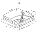
- the lighting device 10 is of the type for use as a backlight for illuminating a liquid crystal display panel (A) such as used in a TV set or a computer display from behind and includes a light guide plate 12, light sources 14, reflectors 16, a reflecting plate 18, a lens sheet 20, and the like.
- A liquid crystal display panel
- the light guide plate 12 is formed from a translucent material such as an acrylic resin and has light entry faces 12a formed on opposite laterals sides thereof, a light emitting face 12b formed on an upper side thereof, and a light non-emitting face 12c formed on a lower side thereof.
- the light emitting face 12b is formed with a plurality of projections 22 each having a smooth hemispherical outward surface forming a hemispherical surface 22a.
- each projection 22 are established so as to become larger and higher as the projection 22 is situated closer to the center of the light emitting face 12b, or to become smaller and lower as the projection 22 is situated closer to an edge of the light emitting face 12b, in order for the amount of light to become even over the entire light emitting face 12b.
- an optical pattern formed by the projections 22 is variable depending upon the shape and the size of the light guide plate 12 and hence is not limited to the optical pattern used in this embodiment.
- the light sources 14 are each disposed to extend along a respective one of the light entry faces 12a of the light guide plate 12.
- the reflecting plate 18 is disposed to extend along the light non-emitting face 12c, while the lens sheet 20 disposed to extend along the light emitting face 12b.
- reflectors 16 are each disposed to cover a respective one of the light sources 14.
- Each of the light sources 14 is adapted to apply light to the entire surface of each light entry face 12a and comprises a cold cathode tube, a fluorescent lamp, a halogen lamp or the like. As shown in Fig. 2, the output power of each light source 14 is established so that the maximum throw of light emitted from each light source 14 becomes substantially equal to distance L from the light source 14 disposed to extend along one light entry face 12a to the other light entry face 12a. This arrangement makes it possible to avoid wasteful consumption of light and hence enhance the efficiency of utilization of light.
- Each of the reflectors 16 is adapted to reflect light emitted from a respective one of the light sources 14 toward a corresponding light entry face 12a and is formed to have a semicylindrical shape using a specularly-reflective material such as a metal foil or an irregularly-reflective material such as a white PET film.
- the reflecting plate 18 is adapted to reflect light leaking from the light guide plate 12 toward the light guide plate 12 and is formed from a specularly-reflective material or an irregularly-reflective material.
- the lens sheet 20 serves to correct the direction of light to a direction substantially perpendicular to the light emitting face 12b of the light guide plate 12 and is formed from a translucent material such as an acrylic resin.
- the lower side of the lens sheet 20, i.e., the side opposite to the light emitting face 12b of the light guide plate 12, is formed with a plurality of first ridges 20a extending parallel with the light entry faces 12a of the light guide plate 12, the first ridges 20a each having a triangular section.
- the first ridges 20a serve to change the direction of light.
- each light source 14 enters the light guide plate 12 from each light entry face 12a either directly or via respective reflector 16 and advances in the light guide plate 12 while being reflected by a wall surface of the light guide plate 12.
- Light in the light guide plate 12 is emitted to the outside through the wall surface when the angle of incident of light on the wall surface of the light guide plate 12 meets a predetermined condition.
- the reflecting plate 18 reflects light leaking from the light non-emitting face 12b to return it into the light guide plate 12.
- Light emitted from the light emitting face 12b becomes incident on the lens sheet 20.
- the direction of light incident on the lens sheet 20 is corrected to a direction perpendicular to the light emitting face 12b by means of the first ridges 20a so that light is applied to the liquid crystal display panel (A).
- Light reflected by the hemispherical surfaces 22a of the projections 22 formed on the light emitting face 12b and light passing through the hemispherical surfaces 22a are regularly directed to advance in a predetermined direction and, hence, there is no loss of light due to scattering of light at the hemispherical surfaces 22a. Further, since light emitted from the hemispherical surfaces 22a is inclined at a predetermined angle (about 70°) relative to the light emitting face 12b as shown in Fig. 3(A), the direction of substantially the whole of light incident on the lens sheet 20 is corrected to the direction perpendicular to the light emitting face 12b by means of the first ridges 20a.
- Y direction a direction parallel with the first ridges 20a
- X direction a direction perpendicular to the first ridges 20a
- light gathered in the X direction provides a narrow viewing angle in the X direction (see Fig. 3(A)) and a wide viewing angle in the Y direction (see Fig. 3(B)) when it is applied to the liquid crystal display panel (A).
- This embodiment is capable of correcting the direction of light by means of the hemispherical surfaces 22a of the light emitting face 12b and the first ridges 20a of the lens sheet 20 both and hence makes it possible to enhance the efficiency of light supply to the liquid crystal display panel (A) by leaps and bounds.
- this embodiment provides a lighting device capable of realizing a higher luminance easily without the need to enhance the output power of the light sources 14 or increase the number of light sources 14. Further, with this embodiment it is possible to downsize the planar light device 10 as well as to reduce the cost significantly.
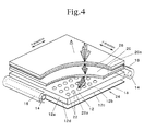
- a planar lighting device 24 shown in Fig. 4 as another embodiment of the present invention is a lighting device improved from the planar lighting device 10 shown in Fig. 1.
- This planar lighting device 24 has a plurality of second ridges 12d formed on light non-emitting face 12c of light guide plate 12, the second ridges 12d each extending in a direction perpendicular to the light entry faces 12a, and a diffuser sheet 26 extending along the upper side, i.e., the light emitting face, of lens sheet 20. Since first ridges 20a of lens sheet 20 are formed to extend parallel with light entry faces 12a, the first ridges 20a and the second ridges 12d extend perpendicular to each other.
- the second ridges 12d may be shaped so that crests and roots alternate continuously as shown in Fig. 4 or intermittently.
- the planar lighting device 24 light incident on the light guide plate 12 is gathered in the Y direction by means of the second ridges 12d. Light thus gathered is emitted from the light emitting face 12b and applied onto the liquid crystal display panel (A) through the lens sheet 20 and the diffuser sheet 26 when a predetermined condition is met. Since light is gathered in the X direction at the lens sheet 20 as described above, this embodiment provides narrow viewing angles in both the X direction and the Y direction, thereby enhancing the luminance in a direction perpendicular to the light emitting face 12b. When light having passed through the lens sheet 20 becomes incident on the diffuser sheet 26, the directionality of light is loosened, so that the intensity of light is rendered even over the entire surface of the diffuser sheet 26.
- a planar lighting device 28 shown in Fig. 5 as yet another embodiment of the present invention is a lighting device improved from the planar lighting device 24 shown in Fig. 4.
- the lighting device 28 has a reflection-type polarizing film 30 disposed to extend along the light emitting face of lens sheet 20.
- the reflection-type polarizing film 30 has a function of allowing one polarized component of incident light (p-polarized light or s-polarized light) to pass therethrough but reflecting the other polarized component (s-polarized light or p-polarized light).
- p-polarized light or s-polarized light a polarized component of incident light
- s-polarized light or p-polarized light s-polarized light or p-polarized light
- Such an arrangement employing reflection-type polarizing film 30 may be applied to Fig. 1 embodiment, or the planar lighting device 10.
- each of the foregoing embodiments has light emitting face 12b formed with plural projections 22 each having an outward surface forming each hemispherical surface 22a, it is possible to provide light emitting face 12b with plural depressions each having an internal surface forming each hemispherical surface 22a instead of the projections 22. Since this arrangement also is capable of regularly directing light so that light advances in a predetermined direction, the lighting device makes it possible to prevent scattering of light and hence provides an enhanced luminance.
- Light guide plate 12 used in each of the foregoing embodiments is characterized in that a plurality of hemispherical surfaces 22a forming optical pattern 23 are formed on light emitting face 12b.
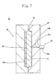
- Such a light guide plate 12 is manufactured using a manufacturing apparatus 32 as shown in Fig. 7.
- the manufacturing apparatus 32 includes a first mold 34, a second mold 36, an injection device 38, and a replica plate 40.
- the first mold 34 together with the second mold 37 defines a cavity 42 and has a lateral side formed with a gate 34a, which communicates with the cavity 42 through a runner 34b extending through the first mold 34.
- the second mold 36 together with the first mold 34 defines the cavity 42 and has an internal face formed with a fitting surface 36a for fitting the replica plate 40 thereon.
- the fitting surface 36a is smooth-finished so as to hold the replica plate 40 stably as well as to prevent the replica plate 40 from deforming.
- Bolt holes are defined at the peripheral edge of the fitting surface 36a for threading engagement with bolts to secure the replica plate 40.
- the first mold 34 and the second mold 36 are fixed to a mold plate not shown and are opened and closed by means of a hydraulic cylinder not shown.
- the injection device 38 is adapted to inject a molten synthetic resin material (acrylic resin or the like) into the cavity 42 and includes an injection nozzle 38a to be connected to the gate 34a.
- a molten synthetic resin material (acrylic resin or the like)
- the replica plate 40 comprises a plate-shaped body 40a of nickel or the like having a surface formed with a pattern 44 corresponding to the optical pattern 23 to be formed on the light emitting face 12b of the light guide plate 12.
- dots 44a forming the pattern 44 are depressions.
- dots 44a forming the pattern 44 are projections.
- the replica plate 40 is fitted to the fitting surface 36a of the second mold 36 with the bolts.
- the replica plate 40 may be fitted to the fitting surface 36a by any other method, such as a method utilizing suction by vacuum or a method employing a stationary frame, than the method using such bolts.
- the first mold 34 and the second mold 36 are closed by means of a hydraulic cylinder not shown, and the injection nozzle 38a of the injection device 38 is connected to the gate 34a of the first mold 34. Then, the injection device 38 injects molten resin into the cavity 42. Since the molten resin fills the cavity 42 conformably with the pattern 44 of the replica plate 40, the resulting molten resin mass has a surface formed with the optical pattern 23, which is the reverse of the pattern 44. After lapse of a predetermined time period from the injection of the molten resin, the first mold 34 and the second mold 36 are opened, and the light guide plate 12 thus molded is released from the molds.
- the inventors of the present invention examined the qualities of respective light guide plates 12 manufactured by varying the thickness t (mm) of a thinnest portion of a 14-inch replica plate 40 and the arithmetic mean roughness h (Ra) of fitting surface 36a and estimated the suitability of each of the light guide plates 12 for practical use. The results are shown in Table 1.
- the thickness t of a thinnest portion of a replica plate 40 having suitability for practical use was 0.8 mm or more. That is, if the thickness t is less than 0.8 mm, the roughness h of the fitting surface 36a has to be 1.5 Ra or less, which requires mirror polishing. This case is not practical from the viewpoints of the cost and time needed for working. If the thickness t is 0.8 mm or more, on the other hand, it is sufficient for the roughness h of the fitting surface 36a to assume 3.2 Ra or more, which does not require mirror polishing. In this case it is possible to reduce the cost for working and shorten the time period needed for working.
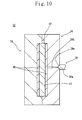
- the method of manufacturing a light guide plate described above employs replica plate 40 having pattern 44 as shown in Fig. 8.
- Such a replica plate 40 is manufactured by the following first method or second method for example.
- a matrix 50 is provided having a plurality of patterns 48 each corresponding to the pattern 44 of an intended replica plate 40 as shown in Fig. 11(A).
- a nickel layer is grown on the surface of the matrix 50 to form a nickel plate 52 by an electroforming process as shown in Fig. 11(B).
- the nickel plate 52 is released from the matrix 50 as shown in Fig. 11(C).
- the nickel plate 52 is then cut to a predetermined size to afford the replica plate 40 as shown in Fig. 11(D).
- the first method employing the electroforming process is capable of forming the pattern 44 of replica plate 40 accurately. Further, the first method is free from a problem that the time period needed for the manufacture becomes too long because the thickness of the thinnest portion of the replica plate 40 is limited to 15 mm or less.
- a plate-shaped material 54 is provided from which replica plate 40 is to be formed, and pattern 44 consisting of plural depressions 58 is formed on the surface of this plate-shaped material 54 with use of a blast nozzle 56 as shown in Fig. 12.
- the blast nozzle 56 is adapted to blast a spherical granular blast material 60 having a diameter of 100 ⁇ m or less (preferably about 10 to about 50 ⁇ m) against the surface of the plate-shaped material 54 at a predetermined pressure.
- the blast nozzle 56 is caused to reciprocate between one lateral side 54a and the other lateral side 54b of the plate-shaped material 54 while pitching within a predetermined width.
- the diameter S and the depth H of each depression 58 formed by the blast nozzle 56 are determined from the diameter and the blasting pressure of the blast material 60, respectively. If the diameter of the blast material 60 is fixed, the diameter S and the depth H increase with increasing blasting pressure or decrease with decreasing blasting pressure.
- the blasting pressure and the pitching width of the blast nozzle 56 are controlled by a control unit not shown to form a blast band (a) having a width corresponding to the pitching width on the surface of the plate-shaped material 54.
- projections 22 need to have gradually increasing diameters and depths as they are situated closer to the center between the opposite light entry faces 12a.
- projections 22 need to have gradually increasing diameters and depths as they are situated away from light entry face 12a and toward an opposite end face. Accordingly, the surface of the plate-shaped material 54 is formed with pattern 44 shown in Fig. 13 or 14 corresponding to one of these optical patterns 23.
- Pattern 44 shown in Fig. 13 corresponds to the optical pattern 23 to be formed on the flat light guide plate 12.
- the blasting pressure of the blast nozzle 56 is gradually increased as the blast nozzle 56 moves from end face 54c of the plate-shaped material 54 toward the center of the material 54.
- pattern 44 shown in Fig. 14 corresponds to the optical pattern 23 to be formed on the wedge-shaped light guide plate 12.
- the blasting pressure of the blast nozzle 56 is gradually increased as the blast nozzle 56 moves from end face 54c of the plate-shaped material 54 toward opposite end face 54d.
- the following blasting pressure control method is employed.
- regions (b1), (b2), ... and (bx+1) including plural blast bands (a) are assumed on the surface of the plate-shaped material 54.
- the amount of change (m1), (m2), ... or (mx + 1) in the blasting pressure against blast bands (a) is set constant.
- the difference ⁇ (mx+1)-(mx) ⁇ between the amounts of changes (mx) and (mx+1) in the blasting pressure applied to adjacent regions (bx) and (bx+1) is limited to 0.02 MPa or lower. Based on these values thus set, the formation of pattern 44 with the blast nozzle 56 is started from the blast band (a) situated closest to end face 54c.
- the relationship between the distance from end face 54c and the blasting pressure in this method can be represented as a graph in Fig. 13 or 14.
- the graph does not largely bend at any boundary between adjacent ones of the regions (b1), (b2), ... (bx+1). This is because the difference between the amounts of changes in blasting pressure is limited to 0.02 MPa or lower.
- light guide plate 12 manufactured by the use of replica plate 40 obtained by this method does not exhibit any steep change in the optical characteristics of its optical pattern 23 and, therefore, liquid crystal display panel (A) is free from any streaky unevenness which would otherwise be caused by light emitted from a conventional light guide plate.
- the inventors of the present invention confirmed the practicality of the second method from the following experiment.
- 210 mm-long replica plate 40 was manufactured. With use of this replica plate 40 wedge-shaped light guide plate 12 was manufactured to examine its optical characteristics.
- blast nozzle 56 was positioned at a location spaced about 200 mm from the surface of the plate-shaped material 54.
- nine regions (b1) to (b9) were assumed on the surface of the plate-shaped material 54, while the amounts of changes in blasting pressure for respective regions (b1) to (b9) were determined.
- the difference between the amounts of changes in the blasting pressure applied to adjacent regions was limited to 0.02 MPa or lower.
- an initial blasting pressure of 0.34 MPa and a pitching width of 2 mm in each region were established. Based on these values thus set, the formation of pattern 44 with the blast nozzle 56 was started from the blast band (a) situated closest to end face 54c as shown in Fig. 12.
- region (b1) extending over a distance of from 0 to 60 mm from end face 54c
- the amount of change in the blasting pressure applied to blast bands (a) was adjusted to 0.002 MPa to form depressions 58.
- region (b2) extending over a distance of from 60 to 90 mm from the end face 54c
- the amount of change in the blasting pressure applied to blast bands (a) was adjusted to 0.003 MPa to form depressions 58. That is, the difference between the amounts of changes in the blasting pressure applied to adjacent regions (b1) and (b2) was adjusted to 0.001 MPa.
- region (b3) extending over a distance of from 90 to 102 mm from the end face 54c, the amount of change in the blasting pressure applied to blast bands (a) was adjusted to 0.005 MPa to form depressions 58.
- region (b4) extending over a distance of from 102 to 114 mm from the end face 54c, the amount of change in the blasting pressure applied to blast bands (a) was adjusted to 0.0075 MPa to form depressions 58. That is, the difference between the amounts of changes in the blasting pressure applied to adjacent regions (b2) and (b3) was adjusted to 0.002 MPa, while the difference between the amounts of changes in the blasting pressure applied to adjacent regions (b3) and (b4) was adjusted to 0.0025 MPa. In this way, all the regions (b1) to (b9) were formed with depressions 58 based on the values shown in Fig. 16.
- Planar lighting device 10 was assembled using light guide plate 12 manufactured with the use of the replica plate 40 thus obtained. Liquid crystal display panel (A) combined with the planar light device 10 did not exhibit any streaky unevenness.
- the relationship between the distance from end face 54c and the blasting pressure according to this method was represented as a graph in Fig. 17.
- the graph did not largely bend at any boundary between adjacent ones of the regions (b1) to (b9).
- the planar lighting device of the present invention is constructed to reflect light regularly at the hemispherical surfaces formed on the light guide plate and allow light to pass through the hemispherical surfaces and hence is capable of minimizing a loss of light due to scattering of light. Since the hemispherical surfaces can be molded integrally with the body portion of the light guide plate, there is no need to provide special parts separately. Thus, the planar lighting device makes it possible to realize a higher luminance easily without incurring an increase in cost as well as to meet the demand for a larger-size screen.
Landscapes
- Physics & Mathematics (AREA)
- General Physics & Mathematics (AREA)
- Optics & Photonics (AREA)
- Nonlinear Science (AREA)
- Mathematical Physics (AREA)
- Chemical & Material Sciences (AREA)
- Crystallography & Structural Chemistry (AREA)
- Planar Illumination Modules (AREA)
- Light Guides In General And Applications Therefor (AREA)
- Liquid Crystal (AREA)
Applications Claiming Priority (8)
| Application Number | Priority Date | Filing Date | Title |
|---|---|---|---|
| JP2001227669A JP2003045213A (ja) | 2001-07-27 | 2001-07-27 | 面型照明装置 |
| JP2001227669 | 2001-07-27 | ||
| JP2001232360A JP2003039487A (ja) | 2001-07-31 | 2001-07-31 | 導光板成形用金型入子の成形表面にシボによるグラデーションパターンを形成する方法 |
| JP2001232360 | 2001-07-31 | ||
| JP2001324017 | 2001-08-22 | ||
| JP2001324017 | 2001-10-22 | ||
| JP2002113497 | 2002-04-16 | ||
| JP2002113497A JP2003202424A (ja) | 2001-10-22 | 2002-04-16 | 導光板の製造方法および製造装置 |
Publications (1)
| Publication Number | Publication Date |
|---|---|
| EP1279892A1 true EP1279892A1 (de) | 2003-01-29 |
Family
ID=27482461
Family Applications (1)
| Application Number | Title | Priority Date | Filing Date |
|---|---|---|---|
| EP02255114A Withdrawn EP1279892A1 (de) | 2001-07-27 | 2002-07-22 | Flache Beleuchtungsvorrichtung |
Country Status (4)
| Country | Link |
|---|---|
| US (1) | US6767105B2 (de) |
| EP (1) | EP1279892A1 (de) |
| KR (1) | KR20030010525A (de) |
| TW (1) | TWI225916B (de) |
Cited By (22)
| Publication number | Priority date | Publication date | Assignee | Title |
|---|---|---|---|---|
| WO2005121844A1 (ja) * | 2004-06-14 | 2005-12-22 | Omron Corporation | 拡散板及び面光源装置 |
| WO2009102733A3 (en) * | 2008-02-12 | 2009-10-15 | Qualcomm Mems Technologies, Inc. | Integrated front light diffuser for reflective displays |
| US7630123B2 (en) | 2004-09-27 | 2009-12-08 | Qualcomm Mems Technologies, Inc. | Method and device for compensating for color shift as a function of angle of view |
| US7710636B2 (en) | 2004-09-27 | 2010-05-04 | Qualcomm Mems Technologies, Inc. | Systems and methods using interferometric optical modulators and diffusers |
| US7750886B2 (en) | 2004-09-27 | 2010-07-06 | Qualcomm Mems Technologies, Inc. | Methods and devices for lighting displays |
| US7777954B2 (en) | 2007-01-30 | 2010-08-17 | Qualcomm Mems Technologies, Inc. | Systems and methods of providing a light guiding layer |
| US7864395B2 (en) | 2006-10-27 | 2011-01-04 | Qualcomm Mems Technologies, Inc. | Light guide including optical scattering elements and a method of manufacture |
| US7933475B2 (en) | 2006-02-17 | 2011-04-26 | Qualcomm Mems Technologies, Inc. | Method and apparatus for providing back-lighting in a display device |
| US8045252B2 (en) | 2004-02-03 | 2011-10-25 | Qualcomm Mems Technologies, Inc. | Spatial light modulator with integrated optical compensation structure |
| US8068710B2 (en) | 2007-12-07 | 2011-11-29 | Qualcomm Mems Technologies, Inc. | Decoupled holographic film and diffuser |
| US8111446B2 (en) | 2004-09-27 | 2012-02-07 | Qualcomm Mems Technologies, Inc. | Optical films for controlling angular characteristics of displays |
| US8231257B2 (en) | 2009-01-13 | 2012-07-31 | Qualcomm Mems Technologies, Inc. | Large area light panel and screen |
| US8348489B2 (en) | 2008-01-30 | 2013-01-08 | Qualcomm Mems Technologies, Inc. | Thin illumination system |
| US8368981B2 (en) | 2006-10-10 | 2013-02-05 | Qualcomm Mems Technologies, Inc. | Display device with diffractive optics |
| US8402647B2 (en) | 2010-08-25 | 2013-03-26 | Qualcomm Mems Technologies Inc. | Methods of manufacturing illumination systems |
| US8674616B2 (en) | 2008-10-10 | 2014-03-18 | Qualcomm Mems Technologies, Inc. | Distributed illumination system |
| US8721149B2 (en) | 2008-01-30 | 2014-05-13 | Qualcomm Mems Technologies, Inc. | Illumination device having a tapered light guide |
| US8872085B2 (en) | 2006-10-06 | 2014-10-28 | Qualcomm Mems Technologies, Inc. | Display device having front illuminator with turning features |
| US8902484B2 (en) | 2010-12-15 | 2014-12-02 | Qualcomm Mems Technologies, Inc. | Holographic brightness enhancement film |
| US8979349B2 (en) | 2009-05-29 | 2015-03-17 | Qualcomm Mems Technologies, Inc. | Illumination devices and methods of fabrication thereof |
| US9019183B2 (en) | 2006-10-06 | 2015-04-28 | Qualcomm Mems Technologies, Inc. | Optical loss structure integrated in an illumination apparatus |
| US9025235B2 (en) | 2002-12-25 | 2015-05-05 | Qualcomm Mems Technologies, Inc. | Optical interference type of color display having optical diffusion layer between substrate and electrode |
Families Citing this family (13)
| Publication number | Priority date | Publication date | Assignee | Title |
|---|---|---|---|---|
| JP2004296215A (ja) * | 2003-03-26 | 2004-10-21 | Toyota Industries Corp | 面状光源用の透明基板、透明基板の製造方法、面状光源及び液晶表示装置 |
| TWI247142B (en) * | 2002-11-20 | 2006-01-11 | Hon Hai Prec Ind Co Ltd | Light guide plate used for backlight module |
| TWI273292B (en) * | 2002-12-31 | 2007-02-11 | Hon Hai Prec Ind Co Ltd | Light guide plate and backlight system using the same |
| JP2005249882A (ja) * | 2004-03-01 | 2005-09-15 | Miyakawa:Kk | 液晶表示装置 |
| JP4093990B2 (ja) * | 2004-05-26 | 2008-06-04 | 日本板硝子株式会社 | 導光体、ライン照明装置および画像読取装置 |
| PL372550A1 (pl) * | 2005-02-02 | 2006-08-07 | Skoff Spółka Z Ograniczoną Odpowiedzialnością | Oprawa oświetleniowa |
| KR100716721B1 (ko) * | 2005-02-18 | 2007-05-09 | 주식회사 우영 | 백라이트 유닛 |
| TW200632455A (en) * | 2005-03-01 | 2006-09-16 | Wintek Corp | Light guide plate |
| JP5011676B2 (ja) * | 2005-08-12 | 2012-08-29 | 株式会社日立製作所 | 表示装置を備える機器 |
| TW200745680A (en) * | 2006-04-19 | 2007-12-16 | Omron Tateisi Electronics Co | Diffuser plate and surface light source device |
| KR101540216B1 (ko) * | 2008-11-03 | 2015-07-29 | 삼성디스플레이 주식회사 | 광학 부재 및 그를 포함하는 표시 장치 |
| WO2011077864A1 (ja) * | 2009-12-23 | 2011-06-30 | シャープ株式会社 | 照明装置、表示装置、及びテレビ受信装置 |
| JP6688744B2 (ja) * | 2014-05-30 | 2020-04-28 | スリーエム イノベイティブ プロパティズ カンパニー | 可変視角を有する光学システム |
Citations (5)
| Publication number | Priority date | Publication date | Assignee | Title |
|---|---|---|---|---|
| US5390276A (en) * | 1992-10-08 | 1995-02-14 | Briteview Technologies | Backlighting assembly utilizing microprisms and especially suitable for use with a liquid crystal display |
| US5863113A (en) * | 1993-06-22 | 1999-01-26 | Mitsubishi Rayon Co., Ltd. | Plane light source unit |
| US5995288A (en) * | 1997-04-22 | 1999-11-30 | Dai Nippon Printing Co., Ltd. | Optical sheet optical sheet lamination light source device, and light-transmissive type display apparatus |
| US5999685A (en) * | 1997-02-07 | 1999-12-07 | Sanyo Electric Co., Ltd. | Light guide plate and surface light source using the light guide plate |
| US20010002165A1 (en) * | 1995-10-13 | 2001-05-31 | Masayuki Shinohara | Image display apparatus |
Family Cites Families (3)
| Publication number | Priority date | Publication date | Assignee | Title |
|---|---|---|---|---|
| JP2630714B2 (ja) * | 1992-10-08 | 1997-07-16 | 茶谷産業株式会社 | 面照明装置 |
| CA2099067C (en) * | 1993-06-23 | 2001-02-13 | Makoto Oe | Plane light source unit |
| JPH11305011A (ja) * | 1998-04-22 | 1999-11-05 | Dainippon Printing Co Ltd | レンズフィルム及び面光源装置 |
-
2002
- 2002-07-12 TW TW091115580A patent/TWI225916B/zh not_active IP Right Cessation
- 2002-07-22 EP EP02255114A patent/EP1279892A1/de not_active Withdrawn
- 2002-07-25 KR KR1020020043782A patent/KR20030010525A/ko not_active Ceased
- 2002-07-26 US US10/205,447 patent/US6767105B2/en not_active Expired - Lifetime
Patent Citations (5)
| Publication number | Priority date | Publication date | Assignee | Title |
|---|---|---|---|---|
| US5390276A (en) * | 1992-10-08 | 1995-02-14 | Briteview Technologies | Backlighting assembly utilizing microprisms and especially suitable for use with a liquid crystal display |
| US5863113A (en) * | 1993-06-22 | 1999-01-26 | Mitsubishi Rayon Co., Ltd. | Plane light source unit |
| US20010002165A1 (en) * | 1995-10-13 | 2001-05-31 | Masayuki Shinohara | Image display apparatus |
| US5999685A (en) * | 1997-02-07 | 1999-12-07 | Sanyo Electric Co., Ltd. | Light guide plate and surface light source using the light guide plate |
| US5995288A (en) * | 1997-04-22 | 1999-11-30 | Dai Nippon Printing Co., Ltd. | Optical sheet optical sheet lamination light source device, and light-transmissive type display apparatus |
Cited By (34)
| Publication number | Priority date | Publication date | Assignee | Title |
|---|---|---|---|---|
| US9025235B2 (en) | 2002-12-25 | 2015-05-05 | Qualcomm Mems Technologies, Inc. | Optical interference type of color display having optical diffusion layer between substrate and electrode |
| US9019590B2 (en) | 2004-02-03 | 2015-04-28 | Qualcomm Mems Technologies, Inc. | Spatial light modulator with integrated optical compensation structure |
| US8045252B2 (en) | 2004-02-03 | 2011-10-25 | Qualcomm Mems Technologies, Inc. | Spatial light modulator with integrated optical compensation structure |
| US8111445B2 (en) | 2004-02-03 | 2012-02-07 | Qualcomm Mems Technologies, Inc. | Spatial light modulator with integrated optical compensation structure |
| US7614776B2 (en) | 2004-06-14 | 2009-11-10 | Omron Corporation | Diffusing board and surface light source device |
| WO2005121844A1 (ja) * | 2004-06-14 | 2005-12-22 | Omron Corporation | 拡散板及び面光源装置 |
| US8111446B2 (en) | 2004-09-27 | 2012-02-07 | Qualcomm Mems Technologies, Inc. | Optical films for controlling angular characteristics of displays |
| US7630123B2 (en) | 2004-09-27 | 2009-12-08 | Qualcomm Mems Technologies, Inc. | Method and device for compensating for color shift as a function of angle of view |
| US7710636B2 (en) | 2004-09-27 | 2010-05-04 | Qualcomm Mems Technologies, Inc. | Systems and methods using interferometric optical modulators and diffusers |
| US7750886B2 (en) | 2004-09-27 | 2010-07-06 | Qualcomm Mems Technologies, Inc. | Methods and devices for lighting displays |
| US8861071B2 (en) | 2004-09-27 | 2014-10-14 | Qualcomm Mems Technologies, Inc. | Method and device for compensating for color shift as a function of angle of view |
| US7933475B2 (en) | 2006-02-17 | 2011-04-26 | Qualcomm Mems Technologies, Inc. | Method and apparatus for providing back-lighting in a display device |
| US8872085B2 (en) | 2006-10-06 | 2014-10-28 | Qualcomm Mems Technologies, Inc. | Display device having front illuminator with turning features |
| US9019183B2 (en) | 2006-10-06 | 2015-04-28 | Qualcomm Mems Technologies, Inc. | Optical loss structure integrated in an illumination apparatus |
| US8368981B2 (en) | 2006-10-10 | 2013-02-05 | Qualcomm Mems Technologies, Inc. | Display device with diffractive optics |
| US7864395B2 (en) | 2006-10-27 | 2011-01-04 | Qualcomm Mems Technologies, Inc. | Light guide including optical scattering elements and a method of manufacture |
| US7777954B2 (en) | 2007-01-30 | 2010-08-17 | Qualcomm Mems Technologies, Inc. | Systems and methods of providing a light guiding layer |
| US8068710B2 (en) | 2007-12-07 | 2011-11-29 | Qualcomm Mems Technologies, Inc. | Decoupled holographic film and diffuser |
| US8798425B2 (en) | 2007-12-07 | 2014-08-05 | Qualcomm Mems Technologies, Inc. | Decoupled holographic film and diffuser |
| US9244212B2 (en) | 2008-01-30 | 2016-01-26 | Qualcomm Mems Technologies, Inc. | Illumination device having a tapered light guide |
| US8721149B2 (en) | 2008-01-30 | 2014-05-13 | Qualcomm Mems Technologies, Inc. | Illumination device having a tapered light guide |
| US8740439B2 (en) | 2008-01-30 | 2014-06-03 | Qualcomm Mems Technologies, Inc. | Thin illumination system |
| US9448353B2 (en) | 2008-01-30 | 2016-09-20 | Qualcomm Mems Technologies, Inc. | Illumination device having a tapered light guide |
| US9395479B2 (en) | 2008-01-30 | 2016-07-19 | Qualcomm Mems Technologies, Inc. | Illumination device having a tapered light guide |
| US8348489B2 (en) | 2008-01-30 | 2013-01-08 | Qualcomm Mems Technologies, Inc. | Thin illumination system |
| US8300304B2 (en) | 2008-02-12 | 2012-10-30 | Qualcomm Mems Technologies, Inc. | Integrated front light diffuser for reflective displays |
| WO2009102733A3 (en) * | 2008-02-12 | 2009-10-15 | Qualcomm Mems Technologies, Inc. | Integrated front light diffuser for reflective displays |
| US8674616B2 (en) | 2008-10-10 | 2014-03-18 | Qualcomm Mems Technologies, Inc. | Distributed illumination system |
| US8231257B2 (en) | 2009-01-13 | 2012-07-31 | Qualcomm Mems Technologies, Inc. | Large area light panel and screen |
| US8439546B2 (en) | 2009-01-13 | 2013-05-14 | Qualcomm Mems Technologies, Inc. | Large area light panel and screen |
| US8979349B2 (en) | 2009-05-29 | 2015-03-17 | Qualcomm Mems Technologies, Inc. | Illumination devices and methods of fabrication thereof |
| US9121979B2 (en) | 2009-05-29 | 2015-09-01 | Qualcomm Mems Technologies, Inc. | Illumination devices and methods of fabrication thereof |
| US8402647B2 (en) | 2010-08-25 | 2013-03-26 | Qualcomm Mems Technologies Inc. | Methods of manufacturing illumination systems |
| US8902484B2 (en) | 2010-12-15 | 2014-12-02 | Qualcomm Mems Technologies, Inc. | Holographic brightness enhancement film |
Also Published As
| Publication number | Publication date |
|---|---|
| TWI225916B (en) | 2005-01-01 |
| US6767105B2 (en) | 2004-07-27 |
| US20030021123A1 (en) | 2003-01-30 |
| KR20030010525A (ko) | 2003-02-05 |
Similar Documents
| Publication | Publication Date | Title |
|---|---|---|
| US6767105B2 (en) | Planar lighting device | |
| US6280043B1 (en) | Surface light source device of side light type | |
| US6652109B2 (en) | Surface light emission device, method of manufacturing the same, and liquid crystal display device | |
| US6502947B2 (en) | Planar light source device and liquid crystal display apparatus | |
| US6734929B2 (en) | Illumination device having a single light source and liquid crystal display device | |
| US7206491B2 (en) | Light guide device and backlight module using the same | |
| US8749729B2 (en) | Light guide plate, surface-emitting apparatus, liquid crystal display apparatus, and method of producing a light guide plate | |
| KR100830261B1 (ko) | 구조화된 면을 구비한 백라이트 | |
| EP2485072A1 (de) | Lichtführungsplatte und Lichtquellenmodul | |
| US20040125592A1 (en) | Backlight device and liquid crystal display device | |
| US7614773B2 (en) | Light guide plate and liquid crystal display device having the same | |
| US20070058391A1 (en) | Light extraction layer | |
| JP2011530090A (ja) | 光透過基板および発光アセンブリおよびその製造方法ならびに光透過基板および発光アセンブリを用いた画像表示方法 | |
| EP1790905A4 (de) | Gegenbeleuchtung von unten | |
| WO2007111829A1 (en) | Illumination apparatus and film | |
| US6486931B1 (en) | LCD optical guide plate with a roughened back surface having projections that support a reflecting sheet | |
| JP2006040710A (ja) | 導光板および該導光板を用いた面型照明装置 | |
| JP2007227405A (ja) | 導光板の製造方法 | |
| KR20050079521A (ko) | 도광판, 백라이트 유닛, 액정디스플레이 및 도광판의제조방법 | |
| US20040212984A1 (en) | Backlight module and light guide plate thereof | |
| US20050111209A1 (en) | Light guide plate, lighting apparatus and liquid crystal display provided with the same, and light guide plate molding die | |
| CN202361194U (zh) | 背光源单元和使用它的影像显示装置 | |
| JP2004192909A (ja) | 導光板及びこの導光板を用いた面光源装置並びにこれを用いた表示装置 | |
| JP2004037982A (ja) | 液晶表示装置 | |
| KR20030094527A (ko) | 도광판, 그 제조 방법, 및 이를 채용하는 면광원장치 |
Legal Events
| Date | Code | Title | Description |
|---|---|---|---|
| PUAI | Public reference made under article 153(3) epc to a published international application that has entered the european phase |
Free format text: ORIGINAL CODE: 0009012 |
|
| AK | Designated contracting states |
Designated state(s): AT BE BG CH CY CZ DE DK EE ES FI FR GB GR IE IT LI LU MC NL PT SE SK TR |
|
| AX | Request for extension of the european patent |
Extension state: AL LT LV MK RO SI |
|
| 17P | Request for examination filed |
Effective date: 20030711 |
|
| AKX | Designation fees paid |
Designated state(s): AT BE BG CH CY CZ DE DK EE ES FI FR GB GR IE IT LI LU MC NL PT SE SK TR |
|
| 17Q | First examination report despatched |
Effective date: 20061019 |
|
| STAA | Information on the status of an ep patent application or granted ep patent |
Free format text: STATUS: THE APPLICATION IS DEEMED TO BE WITHDRAWN |
|
| 18D | Application deemed to be withdrawn |
Effective date: 20081120 |