EP1279923A2 - Méthode et dispositif de contrôle d'un circuit - Google Patents
Méthode et dispositif de contrôle d'un circuit Download PDFInfo
- Publication number
- EP1279923A2 EP1279923A2 EP02002568A EP02002568A EP1279923A2 EP 1279923 A2 EP1279923 A2 EP 1279923A2 EP 02002568 A EP02002568 A EP 02002568A EP 02002568 A EP02002568 A EP 02002568A EP 1279923 A2 EP1279923 A2 EP 1279923A2
- Authority
- EP
- European Patent Office
- Prior art keywords
- edge
- pattern
- roughness
- line
- shape
- Prior art date
- Legal status (The legal status is an assumption and is not a legal conclusion. Google has not performed a legal analysis and makes no representation as to the accuracy of the status listed.)
- Withdrawn
Links
Images





Classifications
-
- G—PHYSICS
- G01—MEASURING; TESTING
- G01N—INVESTIGATING OR ANALYSING MATERIALS BY DETERMINING THEIR CHEMICAL OR PHYSICAL PROPERTIES
- G01N23/00—Investigating or analysing materials by the use of wave or particle radiation, e.g. X-rays or neutrons, not covered by groups G01N3/00 – G01N17/00, G01N21/00 or G01N22/00
- G01N23/22—Investigating or analysing materials by the use of wave or particle radiation, e.g. X-rays or neutrons, not covered by groups G01N3/00 – G01N17/00, G01N21/00 or G01N22/00 by measuring secondary emission from the material
- G01N23/225—Investigating or analysing materials by the use of wave or particle radiation, e.g. X-rays or neutrons, not covered by groups G01N3/00 – G01N17/00, G01N21/00 or G01N22/00 by measuring secondary emission from the material using electron or ion
- G01N23/2251—Investigating or analysing materials by the use of wave or particle radiation, e.g. X-rays or neutrons, not covered by groups G01N3/00 – G01N17/00, G01N21/00 or G01N22/00 by measuring secondary emission from the material using electron or ion using incident electron beams, e.g. scanning electron microscopy [SEM]
-
- G—PHYSICS
- G01—MEASURING; TESTING
- G01N—INVESTIGATING OR ANALYSING MATERIALS BY DETERMINING THEIR CHEMICAL OR PHYSICAL PROPERTIES
- G01N21/00—Investigating or analysing materials by the use of optical means, i.e. using sub-millimetre waves, infrared, visible or ultraviolet light
- G01N21/84—Systems specially adapted for particular applications
- G01N21/88—Investigating the presence of flaws or contamination
- G01N21/95—Investigating the presence of flaws or contamination characterised by the material or shape of the object to be examined
- G01N21/956—Inspecting patterns on the surface of objects
- G01N21/95684—Patterns showing highly reflecting parts, e.g. metallic elements
-
- G—PHYSICS
- G03—PHOTOGRAPHY; CINEMATOGRAPHY; ANALOGOUS TECHNIQUES USING WAVES OTHER THAN OPTICAL WAVES; ELECTROGRAPHY; HOLOGRAPHY
- G03F—PHOTOMECHANICAL PRODUCTION OF TEXTURED OR PATTERNED SURFACES, e.g. FOR PRINTING, FOR PROCESSING OF SEMICONDUCTOR DEVICES; MATERIALS THEREFOR; ORIGINALS THEREFOR; APPARATUS SPECIALLY ADAPTED THEREFOR
- G03F7/00—Photomechanical, e.g. photolithographic, production of textured or patterned surfaces, e.g. printing surfaces; Materials therefor, e.g. comprising photoresists; Apparatus specially adapted therefor
- G03F7/70—Microphotolithographic exposure; Apparatus therefor
- G03F7/70483—Information management; Active and passive control; Testing; Wafer monitoring, e.g. pattern monitoring
- G03F7/70605—Workpiece metrology
- G03F7/70616—Monitoring the printed patterns
-
- G—PHYSICS
- G06—COMPUTING OR CALCULATING; COUNTING
- G06T—IMAGE DATA PROCESSING OR GENERATION, IN GENERAL
- G06T7/00—Image analysis
- G06T7/0002—Inspection of images, e.g. flaw detection
- G06T7/0004—Industrial image inspection
-
- G—PHYSICS
- G06—COMPUTING OR CALCULATING; COUNTING
- G06T—IMAGE DATA PROCESSING OR GENERATION, IN GENERAL
- G06T2207/00—Indexing scheme for image analysis or image enhancement
- G06T2207/30—Subject of image; Context of image processing
- G06T2207/30108—Industrial image inspection
- G06T2207/30148—Semiconductor; IC; Wafer
-
- H—ELECTRICITY
- H01—ELECTRIC ELEMENTS
- H01J—ELECTRIC DISCHARGE TUBES OR DISCHARGE LAMPS
- H01J2237/00—Discharge tubes exposing object to beam, e.g. for analysis treatment, etching, imaging
- H01J2237/26—Electron or ion microscopes
- H01J2237/28—Scanning microscopes
- H01J2237/2813—Scanning microscopes characterised by the application
- H01J2237/2817—Pattern inspection
Definitions
- the present invention relates to a circuit pattern inspection technique and, more particularly, to a method and apparatus for observing a fine pattern by using a scanning microscope and inspecting an edge shape of the fine pattern.
- the occurrence of roughness is caused by the property of the material itself, exposure equipment, a substrate, or an observing apparatus itself.
- the degree of roughness exerts a large influence on the performance of a product.
- appearance of characteristic roughness is often a reflection of deterioration in performance of a manufacturing apparatus, so that a failure may occur in a product in future. Consequently, development of a system for observing the shape of roughness at edges of a pattern and specifying the cause from the characteristic of the roughness is urgently necessary.
- the inspection method has to be a non-destructive one.
- information is empirically obtained mainly by view observation of an observed image by a scanning electron microscope.
- the causes can be considered as follows for example: due to a narrow line, the top of a pattern fluctuates at the time of development, a light intensity distribution at the time of exposure fluctuates, and the observed image itself is distorted.
- roughness is seen relatively small around the surface but is seen large on the bottom portion of a pattern. From such a phenomenon, the possibility that the chemical property of the resist material does not match that of the substrate well and a residual is caused is considered.
- a general method of detecting roughness of a pattern edge is a method of obtaining some deviations of edge positions from a straight line and calculating a standard deviation ⁇ in a distribution of the deviations or a value which is three times as large as ⁇ .
- the roughness herein denotes accurately a dimensional error as used in the documents, "S. Mori, T. Morisawa, N. Matsuzawa, Y. Kamimoto, M. Endo, T. Matsuo, K. Kuhara, and M. Sasago, J. Vac. Sci. Technol. B16, p739 (1998)” and “ C. H. Diaz, H. Tao, Y. Ku, A. Yen, and K. Young, IEEE Electron Device Letters 22, p287 (2001)” and is not an index used to evaluate the shape of an edge.
- An object of the invention is to provide a method and apparatus for circuit pattern inspection capable of converting evaluation of the shape of an edge, which is conventionally performed by view observation of an image into numbers, evaluating the edge shape quantitatively and promptly with high precision, and specifying the cause of occurrence of roughness systematically.
- a data process is directly performed on a two-dimensional distribution image of secondary electrons or reflected electrons obtained by observation with a scanning microscope using a charged particle beam such as an electron beam, ionizing radiation, or an ion particle beam to obtain positions of edge points by a threshold method while keeping the precision of the microscope, and deviations of the edge point positions from an approximation line, that is, edge position fluctuations are computed.
- a set of the edge position fluctuations computed with respect to edge points belonging to one edge expresses a two-dimensional characteristic of the shape of edge roughness.
- the computing operation is performed by using different thresholds to obtain a plurality of sets of edge position fluctuations. By the sets, the shape of the three-dimensional edge roughness of the original image is shown.
- the case where the edge roughness is large around the surface and the case where the edge roughness is large in the bottom portion can be distinguished from each other.
- the cause of occurrence of roughness is an atmosphere during a patterning process.
- the cause is mismatch of the patterned material with an underlayer.
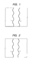
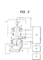
- FIGS. 1 and 2 show examples of the types of the roughness of edges in the case where one line pattern exists in the vertical direction in an image.
- reference numerals 1 and 3 denote left edges of the line, and 2 and 4 indicate right edges.
- FIG. 1 shows a case where the width of the line is constant but the line itself is wavy.
- FIG. 2 shows a case where the right and left edges of the line are synchronous but fluctuate in the opposite directions different from FIG. 1.
- (1) the correlation between the fluctuations in the right and left edge positions is positive.
- (2) the correlation between the fluctuations in the right and left edge positions is negative.
- the right and left edges fluctuate independently, there is no correlation. Concrete calculation and criteria of determination of the coefficient of correlation will be described hereinlater.
- a determining function in which possible steps where roughness is considered to occur are selected based on the calculation results, and a function of displaying them.
- a circuit pattern inspection method of inspecting a pattern shape on the basis of two-dimensional distribution information of intensities of secondary electrons or reflected electrons obtained by observing a pattern formed on a substrate by a scanning microscope using a charged particle beam characterized by including: a step of detecting a set of edge points indicative of positions of edges of the pattern in a two-dimensional plane from the two-dimensional distribution information by a threshold method; a step of obtaining an approximation line for the set of edge points belonging to the edges detected; and a step of obtaining an edge roughness shape by calculating the difference between the set of the edge points and the approximation line.
- a circuit pattern inspection method of inspecting a pattern shape on the basis of two-dimensional distribution information of intensities of secondary electrons or reflected electrons obtained by observing a pattern formed on a substrate by a scanning microscope using a charged particle beam characterized by including: a step of detecting a set of edge points indicative of positions of line edges of the pattern in a two-dimensional plane from the two-dimensional distribution information; a step of obtaining an approximation line for the set of edge points detected for each line edge by least square; a step of obtaining an edge roughness shape by calculating the difference between the set of the edge points belonging to each line edge and the approximation line; and a step of displaying correlation between edge roughness shapes of different line edges.
- the invention is characterized in that, in the above configuration, a plurality of values are used as thresholds used for the threshold method.
- the invention is also characterized in that the above configuration further includes a step of calculating a spatial frequency distribution of the edge roughness shape obtained.
- the invention is also characterized in that the above configuration further includes a step of obtaining the degree of the edge roughness by calculating a standard deviation expressed by the square root of an average of root-mean-square values of the differences each between the set of the edge points derived with respect to the plurality of thresholds and the approximation line.
- the invention is also characterized in that the above configuration further includes a step of selecting a candidate of a process of forming a pattern of the substrate, which causes occurrence of roughness from the edge roughness shape obtained, and displaying the candidate.
- the invention provides a circuit pattern inspection method including: a step of mounting a sample processed in a line pattern shape at a predetermined pitch on a scanning microscope, observing the sample, and obtaining a two-dimensional intensity distribution of secondary electrons or reflected electrons; a step of calculating a shape of roughness of an edge of the line pattern from the two-dimensional intensity distribution; and a step of storing the edge roughness shape obtained as image distortion information of the scanning electron microscope.
- the invention provides a circuit pattern inspection method including: a step of mounting a sample processed in a line pattern shape at a predetermined pitch on a scanning microscope, observing the sample, and obtaining a first two-dimensional intensity distribution of secondary electrons or reflected electrons; a step of moving an observation position in the direction of an edge of the line pattern only by a predetermined length and obtaining a second two-dimensional intensity distribution of secondary electrons or reflected electrons; a step of computing a sum of the first and second two-dimensional intensity distributions; a step of calculating a shape of roughness of an edge of the line pattern from the sum data; and a step of storing the edge roughness shape obtained as image distortion information.
- the above circuit pattern inspection method may further include a step of calculating an image offset amount in the direction perpendicular to an edge of a line pattern in an observation area from the image distortion information obtained and correcting a third two-dimensional intensity distribution of secondary electrons or reflected electrons obtained as a result of observing an arbitrary sample or a pattern edge position obtained from the third two-dimensional intensity distribution.
- the invention provides a circuit pattern inspection apparatus characterized by including: a charged particle source; a charged particle optical system for irradiating a sample with a charged particle beam emitted from the charged particle source through a condenser lens, a deflector, and an object lens, deflecting the beam, and performing the scan with the beam; a stage on which the sample is to be mounted; a detector for detecting intensity of a secondary electron or reflected electron emitted from the sample by irradiation of the charged particle beam; a control system for controlling the deflection and scanning; and signal processing means for obtaining an edge roughness shape and a characteristic of the pattern on the basis of a threshold method from a two-dimensional distribution of intensities of the secondary electrons or reflected electrons obtained.
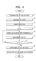
- FIG. 3 is a schematic diagram showing the configuration of an apparatus of the embodiment
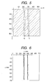
- FIG. 4 is a flowchart showing the procedure of the embodiment
- FIG. 5 is a schematic diagram showing an image formed from data used for evaluation
- FIG. 6 is a diagram showing edges of a line pattern detected with a threshold parameter of 0.5 from the data.
- a sample wafer 11 mounted on a stage 12 in a column 5 is observed.
- An electron beam 7 emitted from an electron emitter 6 of the SEM irradiates the sample wafer 11 on the stage 12 via a condenser lens 8, a deflector 9, and an object lens 10, and a secondary electron 13 emitted from the sample wafer 11 is detected by an electron detector 14.
- the structure of the sample wafer 11 has a line pattern of a resist formed by electron beam drawing on a silicon wafer.
- a sample wafer In the case where there is no record of measurement with respect to a spatial period of edge roughness of the pattern or there is no particular request on the size of an observation area, it is desirable to observe a sample wafer at a magnification of 100,000 times to 300,000 times. In the example, the observation was made at a magnification of 200,000 times.
- the sample wafer 11 was mounted on the stage 12 so that the line pattern is almost perpendicular to the scan direction.
- step 42 scanning is performed a plurality of times, measurement results of the intensities of the secondary electrons emitted from the pattern are added up, and an average value is calculated.
- the desirable number of adding up of data is 64 times or more. In the example, the adding operation was carried out 128 times.
- a distribution of two-dimensional electron intensities obtained in such a manner is data to be analyzed.
- the electron intensity distribution data obtained is converted to shades of a gray scale so as to be displayed as an image on the screen of a terminal of a computer 16 for analysis.
- FIG. 5 is a schematic diagram of the image.
- the image data is composed of 512 pixels in the lateral direction and 512 pixels in the vertical direction.
- the pitch of scan lines corresponding to data in rows can be set to an integral multiple of the pitch of pixels in the lateral direction.
- an area having a width of 675 nm and a length of 2700 nm can be displayed on a screen of 512 ⁇ 512 pixels.
- an observation area included in an image has a length of 675 nm and a width of 675 nm.
- One pixel corresponds to an area having about 1.318-square nm.
- the upper left of an image is set as the origin, a distance to the right is expressed as x, and a distance downward is expressed as y.
- Numbers of pixels in the x and y directions are expressed as m and n, respectively.
- an image having shades according to the intensities of secondary electrons appears.
- an area in which the intensity of a secondary electron is particularly high that is, an area where an edge may exist is expressed as blank and an area having a low intensity of the secondary electron is hatched.
- the coordinates shown in FIG. 5 indicate the numbers of pixels of an image.
- the electron beam is stopped from being continuously emitted to the wafer, after that, the image data is transferred from the control system 15 to the neighboring computer 16.
- the step 42 is finished and the program advances to step 43 where a program for analyzing a shape according to the invention is executed.
- the program performs averaging and smoothing operations on the data as described below to thereby reduce noise.
- the data is divided into a set of 512 intensities of secondary electrons arranged in a line, that is, profiles. Each profile shows dependency on x of the intensity of the secondary electron in the case where y is constant.
- the number of profiles is equal to the number of pixels in the y direction, that is, 512 in total.
- the data is subjected to noise reduction by the following procedure.
- an averaging parameter k 1 (natural number) and a smoothing parameter k 2 (odd number) are given.
- k 1 ' k 1 /2.
- An average of k 1 profiles from the (N-k 1 ')th profile is calculated and used as the n-th profile averaged.
- Smoothing operation using a Hamming window is performed on an area from pixel number m-k 2 ' to pixel number m+k 2 ' in the averaged profile obtained in the preceding step, thereby newly obtaining an m-th value smoothed.
- the averaging parameter k 1 is in a range from 4 to 11
- an area for retrieving edge points is input.
- the calculation areas can be designated by two ways: (1) entry of numerical values, and (2) entry on the screen of FIG. 5. In this example, numerical values were entered.
- the edge points are detected.
- the threshold parameter p for detection is used while being changed from the smallest value p 1 to the largest value p 2 of the set values p at a set pitch of ⁇ p.
- the operation was performed on total 256 profiles whose pixel numbers n in the y direction are even numbers 2n'.
- a threshold method used here is a generally known method in which, from the threshold parameter p and the highest value I max and the lowest value I min of the secondary electron intensity, the threshold obtained by (I max - I min ) ⁇ p + I min is calculated and points at which the intensity of the secondary electron becomes equal to the threshold on the profiles are used as edges.
- X coordinates at the right and left edge points detected are set as x R (2n') and x L (2n'), respectively.
- the profile is a set (x, I (x)) of numerical values I giving the secondary electron intensity at the position to the x coordinate expressed by an integral multiple of the length 1.318 nm of one pixel in the x direction.
- neighboring points are connected with straight lines, and the intersections between the polygonal line and the threshold value are obtained.
- the y coordinate of the edge point obtained in such a manner is 2n' ⁇ 1.318 (unit: nm).
- 256 (x L , y) coordinates can be derived with respect to the left edge.
- a set of 256 points can be obtained with respect to the right edge.
- a process of setting 0.2 as the value of p (step 44), detecting an edge, and increasing the value p by 0.1 is repeated until the value p becomes 0.9 (steps 45 to 47).
- step 48 total 512 points of the right and left edges are approximated by using least square.
- step 49 with respect to a profile obtained when the y coordinate is an even number 2n', the difference between the x coordinate x L (2n') at the left edge point and the intersection of the approximate straight line and the profile, that is, the x coordinate a ⁇ 2n'+b at the approximate point is calculated as an edge point fluctuation ⁇ x L (2n').
- the positions of the points are expressed by x and y in the unit of length of nm. However, the process may be performed by expressing the positions of the points by pixel numbers m and n.
- n is a positive integer, so that a storage capacity to be used can be small.
- Similar calculation is also executed with respect to the right edges, thereby obtaining 256 right edge point fluctuations.
- the program also calculates the values for every threshold. The results of the calculations are stored in the storage area in a computer.
- the shape of edge roughness can be taken out as digital data from a microphotograph expressed in shades of the gray scale and can be displayed as a set of points on a graph. Consequently, the edge shape can be display more clearly.
- An analysis is further conducted by using the data, so that the pattern shape can be analyzed as well.
- edge positions are detected from the image data of a resist pattern shown in FIG. 5 and, further, data indicative of an edge roughness shape is obtained as fluctuations in the edge positions.
- a set of edge position fluctuation data ( ⁇ x L (2n'), 2n') (or a set of ( ⁇ x R (2n'), 2n')) obtained at each threshold is regarded as a summation of periodical functions in the y direction and a distribution of the periods is obtained.
- Fourier transform is performed on a data series ⁇ x L (2), ⁇ x L (4), ⁇ x L (6), ⁇ x L (8), hereby ⁇ to obtain the absolute value of a Fourier coefficient for a spatial frequency (f) in the y direction, that is, the intensity A(f).
- FIG. 7 shows an example of the frequency distribution derived as a result. This is the result of the Fourier transform performed on the left edge of the line illustrated in FIG. 6.
- the characteristic spatial frequency in the frequency distribution is extracted by the following procedure.
- the intensity A(f) in the area of 15 ⁇ f ⁇ 128 is approximated by a function A 0 ⁇ 1/f by using least square, and the function A 0 ⁇ 1/f for which a fitting parameter A 0 obtained is substituted is plotted onto the graph in all of areas where f ⁇ 128.
- the curve expressed by a thick solid line in FIG. 7 is an approximated curve derived in such a manner.
- A(f) as an actually measured value in a preliminarily designated area of (f) is compared with the approximation value A 0 ⁇ 1/f.
- the value (f) at which A(f) is larger than A 0 ⁇ 1/f is picked up.
- the designated area was set as 3 ⁇ f ⁇ 20.
- the space period which can be said as characteristic roughness can be extracted.
- the cause of the edge roughness is resist exposure equipment.
- the cause is the observing apparatus.
- FIGS.5, 8, and 9 A third embodiment of the invention will be described by referring to FIGS.5, 8, and 9.
- edge positions are detected from image data of a resist pattern shown in FIG. 5 and, further, data indicative of the shape of edge roughness is obtained as fluctuations in the edge positions.
- Equation 1 an amount expressed by the following Equation 1, that is, a standard deviation in a fluctuation distribution is calculated, and a value 3 ⁇ which is three times as large as the standard deviation is defined as the degree of edge roughness.
- an index k is equal to L or R.
- This calculation is executed at each threshold, thereby obtaining the relation between the threshold parameter p and the degree of roughness 3 ⁇ with respect to one line edge.
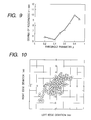
- FIG. 8 shows the result of the calculation executed on the example illustrated in the schematic diagram of FIG. 5. It is understood that the degree of roughness hardly depends on the threshold but is almost constant.
- the graph of the dependency on the threshold parameter p of the degree 3 ⁇ of roughness can be also quantitatively analyzed as follows.
- the value of the obtained fitting parameter (a) is compared with a preset value ⁇ 1 .
- ⁇ 1 it is determined that 3 ⁇ increases as p increases, in other words, roughness is large around the surface.
- the value a is also compared with a preset value ⁇ 2 .
- a ⁇ ⁇ 2 it is determined that 3 ⁇ decreases as p increases, in other words, roughness is large around the bottom of the resist pattern.
- 4 and -4 are standard values as set values of ⁇ 1 and ⁇ 2 , respectively.
- the observer can set other values.
- edge positions are detected from image data of the resist pattern shown in FIG. 5 and, further, data indicative of an edge roughness shape is obtained as fluctuations in the edge positions.
- the numerator of the right side of Equation 2 is the amount expressed by Equation 3.
- ⁇ Co ⁇ ( L,R ) ⁇ L ⁇ R ⁇ L and ⁇ R are standard deviations in the distributions of fluctuations of the left edge position and right edge position, respectively, and each of which corresponds to 1/3 of the degree of roughness.
- ⁇ is calculated as 0.64.
- the type of roughness can be classified as follows.
- the value ⁇ is compared with a preset reference value ⁇ th of the absolute value of ⁇ , and if ⁇ > ⁇ th , the type of FIG. 1 is determined. If ⁇ ⁇ - ⁇ th , the type of FIG. 2 is determined. If none of the cases, it is determined that there is no correlation.
- the graph of dependency of ⁇ on p can be also analyzed quantitatively as follows.
- y is the value ⁇
- x is the threshold p.
- the value of the obtained fitting parameter c is compared with a preset value ⁇ 1 .
- ⁇ increases as p increases. That is, it is determined that the correlation between the right and left edge fluctuations is higher around the surface.
- ⁇ is compared with a preset value ⁇ 2 , if c ⁇ 2 , ⁇ decreases as p increases. That is, it is determined that correlation between the right and left edge fluctuations is larger around the bottom of the resist pattern.
- the set values ⁇ 1 and ⁇ 2 , 0.4 and -0.4 are standard values, respectively. Although the observer can set other values, in the example, the inspection was conducted by using the standard values.
- FIGS. 1 to 3 A fifth example of the invention will be described by referring to FIGS. 1 to 3, FIGS. 5 to 8, FIGS. 10, 11, 13, and 14.
- FIG. 14 shows the details of a part of step 139 in the flow of FIG. 13.
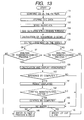
- a line pattern is observed with a scanning microscope and data is captured (steps 131 and 132).
- Acquired two-dimensional data is subjected to noise reduction by the method described in the first embodiment (step 133), and the shape of edge roughness is obtained by using a standard value p (usually, 0.5) (step 134) .
- the degree (3 ⁇ ) of roughness given by Equation 1 is calculated (step 135).
- the program advances to step 136 and whether a wafer is good or not is determined. Only in the case where 3 ⁇ of all of the edges measured is smaller than a reference value, a wafer with a pattern to be observed is determined as good and passed to the following process. It is also possible to select whether the shape analysis in step 139 and subsequent steps is performed or not irrespective of the result of the determination (steps 137 and 138). If NO, the inspection on the wafer to be observed is finished. A good wafer is passed to the next step and a non-conforming wafer is taken out from the lot.
- the program advances to step 139 where a line to be observed is selected from two-dimensional data of which noise has been reduced, and edge detection is sequentially performed by using a plurality of thresholds as described in the first embodiment to obtain data of an edge roughness shape with respect to each of the thresholds.
- the data process includes three kinds of inspections for showing the characteristic of the edge shape and any of the inspections desired is selected (step 147). Although it is desirable to select all of the processes to obtain a result with high reliability, two or even one of the processes may be executed to shorten the execution time. The details of steps 148 to 150 will be described hereinbelow.
- the first process is calculation of the space frequency showing the characteristic of the edge roughness shape.
- the spatial frequency distribution is calculated by a method described in the second embodiment and, after that, characteristic spatial frequencies common to the spatial frequency distribution of the edge roughness shapes at all the thresholds are picked up (step 148).
- the second process is calculation of the dependency on the threshold of the degree of roughness.
- the dependency is calculated by the method described in the third embodiment (step 149).
- the third process is calculation of a graph indicative of the correlation between right and left edge fluctuations belonging to one line with respect to thresholds, and calculation of dependency on the threshold of the correlation coefficient of the right and left edge fluctuations. They are calculated by the method described in the fourth embodiment (steps 150 and 151).
- step 152 Analysis results of the items are displayed (step 152). After that, as shown in step 140 in FIG. 13, whether the roughness causing process is specified automatically or not is selected. In the case of NO, if necessary, the above result is examined by the observer and the inspection on the wafer to be observed is finished. The wafer is processed according to the result of the determination of conformity (step 144). In the case of automatically specifying the roughness causing process, by checking the result with the reference in step 141, the program determines whether or not there is the possibility that any of the pattern generating processes causes the roughness and outputs the result.
- steps 142 and 143 a signal is sent to the fabricating apparatus in accordance with the result, the inspection on the wafer to be observed is finished, and the wafer is processed according to the determination of conformity (steps 144 to 146).
- the inspection performed in the example will be concretely described hereinbelow.
- an image of a line pattern of an electron beam resist shown in the schematic view of FIG. 5 is inspected by using the apparatus shown in FIG. 3.
- the resist used for generating the pattern is a negative type.
- the shapes are as shown in FIG. 6.
- the degree of the right and left edge roughness is calculated by using the data and displayed together with the image.
- the sample to be observed is subjected to the determination of conformity and determined as a good item.
- the reference value of the roughness of the conforming item in the inspection is set to 6 nm. In the case where the sample is determined as a defective, an alarm sound is generated and the numerical values of roughness larger than the reference value are displayed in red in an image. The numerical values equal to or smaller than the reference value are displayed in white or black.
- the correlation of the right and left edge roughness shapes was calculated as a coefficient of correlation, and the dependency on the threshold p of the coefficient of correlation was calculated.
- graphs shown in FIGS. 10 and 11 were obtained and it was found that the coefficient of correlation is positive and larger than the reference value, that is, the fluctuations are of the type shown in FIG. 1, and the tendency does not depend on the threshold p.
- the observer displayed the results and operated the automatic determining function of determining the roughness causing process.
- the procedure of narrowing candidates of the roughness causing process of a resist of a general automatic determining program will be described hereinbelow.
- setting of values such as ⁇ 1 and ⁇ 2 used for the determining methods setting of a reference used to narrow the candidates, and setting of exceptions, not only the general reference values used in the example but also data accumulated by the user are helpful. With them, roughness of a pattern of something other than the resist can be also inspected.
- a memory device is provided for the computer in order to accumulate data.
- (2) indicates edge roughness of a reticle pattern or a position or strong fluctuation of a beam at the time of drawing.
- (3) indicates distortion of a whole line due to swelling caused by mismatch of the density of a developer or an eddy of the developer.
- (4) indicates erosion of the surface of a pattern by amine or acids in the atmosphere.
- (5) indicates footing due to the chemical nature such as insufficient processing on the surface of the substrate.
- (6) indicates unevenness of reflectance due to a lower layer pattern.
- (7) indicates distortion of an image due to electric noise or vibration.
- the cause of the edge roughness shown in FIG. 5 was determined as (2) or (7).
- the observed wafer was sent as a conforming item to the following process, and the inspection was once finished.
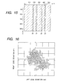
- FIG. 15 is a concept diagram showing an image of data used for evaluation.
- FIG. 16 is a graph showing the correlation of right and left edge position fluctuations of a line pattern observed.
- the pattern shape was evaluated and determined by using the apparatus shown in FIG. 3 in accordance with the same flow as that of the fifth embodiment.
- a line pattern of a positive type ArF resist formed on a silicon wafer is observed by ArF lithography on the sample wafer 11.
- the magnification is desirably 100,000 times or less. In the example, the observation was made at the magnification of 100,000 times.
- the line pattern to be observed is mounted in the direction almost perpendicular to the scan direction.
- the observation area has a length of 1.35 ⁇ m in the direction perpendicular to the line pattern and a length of 5.40 ⁇ m in the direction parallel to the line pattern, and the distance between neighboring scan lines is 10.55 nm.
- the aspect ratio of the observation area is 2:1 or higher. Since the length in the vertical direction of the area to be observed was 6 ⁇ m in the example, 4:1 was set. After scanning 64 times, the measurement results of intensity of secondary electrons emitted from the pattern were added up, the average value was used as shades of the gray scale, and the shades were displayed as an image on the screen of the control system 15.
- FIG. 15 is a schematic diagram of an image appeared on the screen.
- the image data is constructed by 512 pixels in the lateral direction and 512 pixels in the vertical direction. It is assumed that the upper left point of the image is the origin, the distance to the right is expressed as (x), and the distance to the left is expressed as (y).
- the number of each of pixels in the (x) direction is expressed as (m)
- the number of each of pixels in the (y) direction is expressed as (n).
- the area of one pixel has an area having a length of 2.637 nm in the x direction and a length of 10.55 nm in the y direction. In reality, an image having shades according to the intensities of secondary electrons appears. In FIG. 15, areas where the intensity of secondary electrons is high, that is, an edge can exist are expressed in white, and areas in which the intensity of secondary electrons is low are hatched.
- the coordinates shown in FIG. 15 express the image pixel numbers.
- the image data was transferred from the control system 15 to the computer 16 adjacent to the control system 15.
- a program for conducting an inspection according to the invention was executed from a terminal of the computer 16.
- the program processed an image file converted to the numerical value data of 512 ⁇ 512 pixels by using the threshold method described in the first embodiment, and the coordinates of edge points of total four edges of two lines existing in the image were detected.
- the averaging parameter was set to 4
- the smoothing parameter was set to 3.
- Calculation was executed on all of profiles, that is, 512 profiles, and the threshold p was set to 0.5.
- An entered edge retrieval area was set as follows.
- a fluctuation in the left edge point of the first line obtained with respect to a profile whose y coordinate is an integer (n) is described as ⁇ x 1L (n) and a fluctuation in the right edge point is described as ⁇ x 1R (n). Fluctuations on all of profiles having n of 1 to 512 were calculated.
- the spatial frequency analysis as the first inspection item was performed on the total four edges of both right and left edges of the first and second lines.
- FIG. 16 shows a graph of the correlation between the right and left edges in the first line when p is 0.5.
- the function of determining the roughness causing process was executed here.
- a warning of an abnormal appearance of a pattern in the underlayer as the cause (6) of roughness described in the fifth embodiment was displayed and an instruction to temporarily stop the lithography process performed on the substrate and make a check was given.
- the details of the warning were displayed, and the possibility that periodic patterns exist in the underlayer substrate at a pitch of 0.7 to 0.9 ⁇ m and cause a unevenness of reflectance was pointed out.
- a signal is sent from the computer 16 to a lithography system 17 to stop the lithography process, the processes before the lithography were also temporarily stopped, and the history of the substrate was referred to. It was recognized that metal line patterns exist in the substrate in the direction perpendicular to the line pattern observed, and the pitch of the metal line patterns was 0.8 ⁇ m. It is estimated that, in an area on the metal line patterns, antireflection is imperfect, and the line pattern of the resist was consequently narrowed. Based on the estimation, antireflection was thoroughly performed. After that, such a phenomenon stopped appearing, and the yield was improved. By temporarily stopping the processes in response to the warning, the number of wafers going back to fabrication of an antireflection film could be minimized.
- FIG. 17 is a flowchart for acquiring image distortion data.
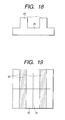
- FIG. 18 is a schematic cross section of a sample used.
- FIG. 19 is a schematic diagram showing the screen of a microscope showing arrangement of the sample at the time of observation.
- FIG. 20 is a graph showing an image distortion amount obtained.
- FIG. 19 is a diagram of the structure observed from above, having a line and space shape. Since the magnification of 100,000 times or higher is desired for measuring edge roughness of a line pattern and it is necessary to observe the edges of at least two line patterns by the method, the pitch of the line-and-space pattern formed on the standard sample is desirably 0.5 ⁇ m or less. The ratio of the line width to the space width is desirably 1 or less.
- a sample having a pitch of 0.24 ⁇ m and the line width of 0.10 ⁇ m was used and observed at the magnification of 200,000 times.
- the area to be observed was a square area of 675 ⁇ 675 nm.
- the result of observation that is, the intensity distribution of detected secondary electrons, was displayed as shades of the gray scale on pixels in corresponding portions.
- the observed area is displayed as an image of 512 ⁇ 512 pixels.
- the sample was mounted so that the center of a space part 25 between two lines 24 almost coincides with a vertical axis 26 indicative of the center of the observation area.
- the edge direction of the line pattern was so arranged to be in parallel with the vertical axis 26 by view observation.
- a storage area for taking in image data in the control system 15 in the scanning electron microscope was initialized to set all values to "0".
- the following first and second procedures were performed repeatedly (corresponding to an operation of performing steps 172 and 174, and returning again to step 171).
- step 172 First, scanning was performed eight times with the scanning electron microscope, the intensities of secondary electrons emitted from the sample were added up, and the average value was calculated and added to the memory area of the control system (step 172). Second, the irradiation of an electron beam was stopped and a check is made to see whether or not the scan has reached the repetition number of times which has been set (step 173). If "Yes”, the program advances to the following step 175. If "No", the scan position is moved upward in the screen by an amount of eight pixels , that is, 10.55 nm (step 174). The number of repetition times was set 128. It took about 40 seconds to integrate 128 average image data of eight scans. Desirably, the number of scans in the first procedure is at least four in order to reduce noise.
- observation area of the first time and that of the last time are not overlapped with each other, so that the product between the movement distance in the second procedure and the number of times for repeating the first and second procedures is preferably set to be equal to or larger than the length in the vertical direction of the area which can be observed at a time.
- the upper left point of an image is set as an origin
- the distance to the right side is (x)
- the distance to the below is (y).
- the numbers of pixels in the x and y directions are expressed by (m) and (n), respectively.
- step 175. The obtained 512 ⁇ 512 two-dimensional data array is dealt as data of one image, and noise was reduced by the method described in the first embodiment (step 175).
- the edge detection and calculation of an approximation line were performed by the threshold method (step 176). The detection was performed on the right and left edges of the first and second lines in an image. Each of the averaging parameter and the smoothing parameter was set to 11. 0.5 was used as the threshold parameter. Detection was performed on all the profiles and 512 edge points were calculated per edge. From the data, a set of edge point fluctuations was obtained (step 177) . Further, as a reference, the degree of edge roughness, that is, 3 ⁇ was calculated by Expression 1. The program may advance to step 178 without calculating 3 ⁇ .
- the purpose was to detect image distortions caused by an influence of an apparatus having a power source disposed near the scanning microscope or a power supply cable.
- the image distortions appear in an area where the spatial frequency is 20 or lower in an image.
- the spatial frequency of 20 is converted to a space period, about 25 pixels are derived. Consequently, numerical values equal to or lower than 25 have to be used as the averaging parameter and the smoothing parameter.
- edges were obtained.
- the data of one edge is constructed by position coordinates of the 512 edge points.
- the edges are not actually existing edges but are obtained by averaging actual edge data in the y direction by the above method. Therefore, roughness which occurs at random in the lines observed is eliminated by the averaging.
- the degree 3 ⁇ of roughness of the edge data was about 3 to 4 nm.
- the value is large as a noise, and there is the possibility that the microscope image itself is distorted.
- the coefficient of correlation of the right and left edge roughness was computed by the method described in the fourth embodiment, and 0.68 was obtained.
- the coefficient of correlation of the right and left edge roughness of the second line was also high as 0.55.
- the coefficient of correlation between edges belonging to different lines were computed.
- the combinations are (1) the left edges of the first and second lines, (2) the left edge of the first line and the right edge of the second line, (3) the right edge of the first line and the left edge of the second line, and (4) the right edges of the first and second lines. All the coefficients of correlation computed were equal to or higher than 0.5. It means that the whole image is distorted but is seen like a part of the profiles is parallel-translated in the x direction. Consequently, it was determined in step 179 that the image has to be corrected.
- FIG. 20 shows a graph of an image distortion amount ⁇ x(n) with respect to an obtained line profile number (n). It is also possible to regard the roughness of an edge close to the center as an image distortion amount without averaging data of the four edges .
- the data of the image distortion amount obtained was recorded in a file (step 180).
- a file of image distortion data ⁇ x(n) at each of the magnifications is generated by the above procedure and, by using the file, an image distortion was corrected by the above method.
- the invention can be also applied to a case using a two-dimensional distribution of particles such as reflected electrons which are emitted secondarily from a sample.
- the invention can be also applied to cases of observation by a scanning microscope using a charged particle beam such as an ion particle beam or ionizing radiation or, further, light.
- the three-dimensional shape of a pattern edge can be expressed in numerical value data.
- Degree of roughness in the direction along a line, a wavy state of a line, and the difference in the roughness shape between a bottom portion and a portion around the surface of a pattern can be quantitatively expressed.
- candidates of processes as a main cause of roughness are selected, and the fabricating process of a semiconductor device or a micromachine can be controlled.
- An image distortion of the microscope itself used for observation can be also extracted and eliminated from an arbitrary image by a simple, cheap method.
- the method and apparatus for circuit pattern inspection capable of converting the evaluation of characteristics of edge shape, which is conventionally visually observed, into values, performing analysis quantitatively and promptly with high precision, and specifying the cause of occurrence of roughness systematically can be realized. Further, by using the method and apparatus to control the fabricating process or fabricating apparatus causing the roughness, a super minute patterning process is managed, so that improvements in yield and throughput can be expected.
Landscapes
- General Physics & Mathematics (AREA)
- Physics & Mathematics (AREA)
- Engineering & Computer Science (AREA)
- Immunology (AREA)
- Analytical Chemistry (AREA)
- Biochemistry (AREA)
- General Health & Medical Sciences (AREA)
- Chemical & Material Sciences (AREA)
- Life Sciences & Earth Sciences (AREA)
- Pathology (AREA)
- Health & Medical Sciences (AREA)
- Quality & Reliability (AREA)
- Computer Vision & Pattern Recognition (AREA)
- Theoretical Computer Science (AREA)
- Length-Measuring Devices Using Wave Or Particle Radiation (AREA)
- Testing Or Measuring Of Semiconductors Or The Like (AREA)
Applications Claiming Priority (2)
| Application Number | Priority Date | Filing Date | Title |
|---|---|---|---|
| JP2001224017A JP3870044B2 (ja) | 2001-07-25 | 2001-07-25 | パターン検査方法及びパターン検査装置 |
| JP2001224017 | 2001-07-25 |
Publications (2)
| Publication Number | Publication Date |
|---|---|
| EP1279923A2 true EP1279923A2 (fr) | 2003-01-29 |
| EP1279923A3 EP1279923A3 (fr) | 2007-10-10 |
Family
ID=19057258
Family Applications (1)
| Application Number | Title | Priority Date | Filing Date |
|---|---|---|---|
| EP02002568A Withdrawn EP1279923A3 (fr) | 2001-07-25 | 2002-02-04 | Méthode et dispositif de contrôle d'un circuit |
Country Status (3)
| Country | Link |
|---|---|
| US (2) | US7095884B2 (fr) |
| EP (1) | EP1279923A3 (fr) |
| JP (1) | JP3870044B2 (fr) |
Cited By (2)
| Publication number | Priority date | Publication date | Assignee | Title |
|---|---|---|---|---|
| WO2005059531A1 (fr) * | 2003-12-10 | 2005-06-30 | Applied Materials Israel, Ltd. | Metrologie de rugosite avancee |
| CN101986099A (zh) * | 2010-10-21 | 2011-03-16 | 中国林业科学研究院木材工业研究所 | 一种确定材料边缘的方法和系统 |
Families Citing this family (41)
| Publication number | Priority date | Publication date | Assignee | Title |
|---|---|---|---|---|
| KR100492153B1 (ko) * | 2002-10-30 | 2005-06-02 | 삼성전자주식회사 | 고속 퓨리에 변환 기법을 이용한 분석 방법 및 장치 |
| US6934929B2 (en) * | 2003-01-13 | 2005-08-23 | Lsi Logic Corporation | Method for improving OPC modeling |
| JP4364524B2 (ja) * | 2003-02-20 | 2009-11-18 | 株式会社日立製作所 | パターン検査方法 |
| US7136506B2 (en) * | 2003-03-03 | 2006-11-14 | Lockheed Martin Corporation | Correlation based in frame video tracker |
| JP3960601B2 (ja) * | 2003-03-19 | 2007-08-15 | 株式会社東芝 | エッジ位置ずれ量の算出方法、検証方法、検証プログラム、及び検証システム。 |
| JP4286657B2 (ja) | 2003-12-26 | 2009-07-01 | 株式会社日立ハイテクノロジーズ | 走査電子顕微鏡を用いたライン・アンド・スペースパターンの測定方法 |
| JP4262125B2 (ja) * | 2004-03-26 | 2009-05-13 | 株式会社日立ハイテクノロジーズ | パターン測定方法 |
| US20050275850A1 (en) * | 2004-05-28 | 2005-12-15 | Timbre Technologies, Inc. | Shape roughness measurement in optical metrology |
| JP2006038779A (ja) * | 2004-07-30 | 2006-02-09 | Hitachi High-Technologies Corp | パターン形状評価方法、評価装置、及び半導体装置の製造方法 |
| JP4801427B2 (ja) * | 2005-01-04 | 2011-10-26 | 株式会社日立ハイテクノロジーズ | パターン形状評価方法 |
| JP4801795B2 (ja) * | 2005-01-04 | 2011-10-26 | 株式会社日立ハイテクノロジーズ | パターン形状評価方法及び電子顕微鏡 |
| US7348556B2 (en) * | 2005-07-19 | 2008-03-25 | Fei Company | Method of measuring three-dimensional surface roughness of a structure |
| JP2006234808A (ja) * | 2006-02-15 | 2006-09-07 | Hitachi Ltd | 計測システム |
| JP2007219208A (ja) * | 2006-02-17 | 2007-08-30 | Sony Corp | パターン補正装置、パターン補正プログラム、パターン補正方法および半導体装置の製造方法 |
| JP4922710B2 (ja) * | 2006-09-20 | 2012-04-25 | 株式会社日立ハイテクノロジーズ | 電子顕微鏡の分解能評価用試料及び電子顕微鏡の分解能評価方法並びに電子顕微鏡 |
| JP2008233343A (ja) * | 2007-03-19 | 2008-10-02 | Advanced Mask Inspection Technology Kk | 試料検査装置、補正画像生成方法及びプログラム |
| US7796804B2 (en) * | 2007-07-20 | 2010-09-14 | Kla-Tencor Corp. | Methods for generating a standard reference die for use in a die to standard reference die inspection and methods for inspecting a wafer |
| JP5216274B2 (ja) * | 2007-08-17 | 2013-06-19 | 株式会社日立ハイテクノロジーズ | パターン評価方法及びその装置 |
| JP2008116472A (ja) * | 2008-01-07 | 2008-05-22 | Hitachi Ltd | パターン検査方法 |
| JP4898713B2 (ja) * | 2008-01-17 | 2012-03-21 | 株式会社日立ハイテクノロジーズ | 表面検査装置および表面検査方法 |
| JP4926116B2 (ja) * | 2008-04-16 | 2012-05-09 | 株式会社日立ハイテクノロジーズ | 画像検査装置 |
| JP5337458B2 (ja) * | 2008-11-19 | 2013-11-06 | 株式会社日立ハイテクノロジーズ | パターン形状検査方法及びその装置 |
| DE102009015594B4 (de) * | 2009-03-30 | 2015-07-30 | Carl Zeiss Sms Gmbh | Verfahren und Vorrichtung zur subpixelgenauen Positionsbestimmung einer Kante einer Markerstruktur in einer Vielzahl von Aufnahmepixeln aufweisenden Aufnahme der Markerstruktur |
| JP5500858B2 (ja) * | 2009-04-14 | 2014-05-21 | 株式会社日立ハイテクノロジーズ | パターン測定装置 |
| DE112009002638T5 (de) * | 2009-10-30 | 2012-05-16 | Advantest Corp. | Strukturmessgerät und Strukturmessverfahren |
| JP5386446B2 (ja) * | 2010-07-13 | 2014-01-15 | 株式会社日立ハイテクノロジーズ | 画像データ解析装置 |
| KR20120035422A (ko) * | 2010-10-05 | 2012-04-16 | 삼성전자주식회사 | 반도체 소자의 이미지 형성 방법, 이를 이용한 반도체 소자의 결함 검사 방법 |
| TWI475187B (zh) | 2010-10-27 | 2015-03-01 | 日立全球先端科技股份有限公司 | Image processing devices and computer programs |
| JP6101445B2 (ja) * | 2012-08-03 | 2017-03-22 | 株式会社日立ハイテクノロジーズ | 信号処理装置及び荷電粒子線装置 |
| JP2014035326A (ja) * | 2012-08-10 | 2014-02-24 | Toshiba Corp | 欠陥検査装置 |
| JP6129651B2 (ja) * | 2013-06-11 | 2017-05-17 | 株式会社日立ハイテクノロジーズ | ラインパターンの形状評価方法及びその装置 |
| KR102152301B1 (ko) * | 2015-12-04 | 2020-09-07 | 에이에스엠엘 네델란즈 비.브이. | 메트롤로지 데이터로부터의 통계적 계층 재구성 |
| KR102582665B1 (ko) * | 2016-10-07 | 2023-09-25 | 삼성전자주식회사 | 집적 회로의 패턴들을 평가하는 시스템 및 방법 |
| US10622266B2 (en) | 2017-04-04 | 2020-04-14 | Globalfoundries Inc. | Methods of identifying space within integrated circuit structure as mandrel space or non-mandrel space |
| JP2019039884A (ja) | 2017-08-29 | 2019-03-14 | 株式会社日立ハイテクノロジーズ | パターン測定方法、及びパターン測定装置 |
| JP6751062B2 (ja) * | 2017-09-13 | 2020-09-02 | 株式会社日立製作所 | 自動点検システムおよび自動点検方法 |
| JP7011562B2 (ja) | 2018-09-25 | 2022-01-26 | 株式会社日立ハイテク | パターン形状評価装置、パターン形状評価システム及びパターン形状評価方法 |
| JP2022112303A (ja) | 2021-01-21 | 2022-08-02 | 株式会社日立ハイテク | パターン測定システム、パターン測定方法、およびプログラム |
| WO2024180710A1 (fr) * | 2023-03-01 | 2024-09-06 | 株式会社日立ハイテク | Procédé de mesure de dispositif à semi-conducteur, système de mesure de dispositif à semi-conducteur et appareil d'affichage |
| CN117011285A (zh) * | 2023-09-01 | 2023-11-07 | 上海精测半导体技术有限公司 | 基于扫描电镜图像的线粗糙度量测方法 |
| CN119693492B (zh) * | 2024-11-06 | 2025-09-23 | 北京智芯微电子科技有限公司 | 集成电路合成扫描电镜图生成方法、装置、设备及介质 |
Family Cites Families (11)
| Publication number | Priority date | Publication date | Assignee | Title |
|---|---|---|---|---|
| CA1240052A (fr) * | 1984-11-30 | 1988-08-02 | Motoji Shiozumi | Methode et dispositif pour evaluer le degre de brillance d'un objet |
| US4792232A (en) * | 1987-05-18 | 1988-12-20 | Shell Oil Company | Method and apparatus for detection of undesirable surface deformities |
| JP3317030B2 (ja) | 1994-06-27 | 2002-08-19 | ヤマハ株式会社 | 寸法測定装置 |
| KR100187346B1 (ko) * | 1994-08-22 | 1999-05-01 | 모리시타 요이찌 | 에지라인 측정방법 |
| JP4130012B2 (ja) | 1998-08-03 | 2008-08-06 | 株式会社ルネサステクノロジ | 走査型荷電粒子線応用装置ならびにそれを用いた顕微方法および半導体装置製造方法 |
| JP2001093803A (ja) * | 1999-09-20 | 2001-04-06 | Sony Corp | リソグラフィーにおけるボケ量の算出方法及びリソグラフィー方法 |
| JP2001183116A (ja) | 1999-12-24 | 2001-07-06 | Toppan Printing Co Ltd | マスクパターン形状計測方法 |
| JP3842944B2 (ja) | 2000-02-07 | 2006-11-08 | フジノン株式会社 | 電子内視鏡の電気マスク生成装置 |
| US6433348B1 (en) * | 2000-07-25 | 2002-08-13 | Applied Materials, Inc. | Lithography using multiple pass raster-shaped beam |
| JP4090683B2 (ja) * | 2000-11-27 | 2008-05-28 | 株式会社東芝 | パターン評価方法、パターン評価装置およびコンピュータ読み取り可能な記録媒体 |
| US6781688B2 (en) * | 2002-10-02 | 2004-08-24 | Kla-Tencor Technologies Corporation | Process for identifying defects in a substrate having non-uniform surface properties |
-
2001
- 2001-07-25 JP JP2001224017A patent/JP3870044B2/ja not_active Expired - Lifetime
-
2002
- 2002-02-04 EP EP02002568A patent/EP1279923A3/fr not_active Withdrawn
- 2002-02-11 US US10/071,097 patent/US7095884B2/en not_active Expired - Lifetime
-
2006
- 2006-08-10 US US11/501,843 patent/US7369703B2/en not_active Expired - Lifetime
Non-Patent Citations (2)
| Title |
|---|
| C. H. DIAZ; H. TAO; Y. KU; A. YEN; K. YOUNG, IEEE ELECTRON DEVICE LETTERS, vol. 22, 2001, pages 287 |
| S . MORI; T. MORISAWA; N. MATSUZAWA; Y. KAMIMOTO; M. ENDO; T. MATSUO; K. KUHARA; M. SASAGO, J. VAC. SCI. TECHNOL., vol. B16, 1998, pages 739 |
Cited By (4)
| Publication number | Priority date | Publication date | Assignee | Title |
|---|---|---|---|---|
| WO2005059531A1 (fr) * | 2003-12-10 | 2005-06-30 | Applied Materials Israel, Ltd. | Metrologie de rugosite avancee |
| US8340393B2 (en) | 2003-12-10 | 2012-12-25 | Applied Materials Israel Limited | Advanced roughness metrology |
| CN101986099A (zh) * | 2010-10-21 | 2011-03-16 | 中国林业科学研究院木材工业研究所 | 一种确定材料边缘的方法和系统 |
| CN101986099B (zh) * | 2010-10-21 | 2013-11-06 | 中国林业科学研究院木材工业研究所 | 一种确定材料边缘的方法和系统 |
Also Published As
| Publication number | Publication date |
|---|---|
| EP1279923A3 (fr) | 2007-10-10 |
| JP2003037139A (ja) | 2003-02-07 |
| US7095884B2 (en) | 2006-08-22 |
| US20030021463A1 (en) | 2003-01-30 |
| JP3870044B2 (ja) | 2007-01-17 |
| US20060269121A1 (en) | 2006-11-30 |
| US7369703B2 (en) | 2008-05-06 |
Similar Documents
| Publication | Publication Date | Title |
|---|---|---|
| US7095884B2 (en) | Method and apparatus for circuit pattern inspection | |
| JP7402061B2 (ja) | 試験片の調査の方法およびそのシステム | |
| JP4801427B2 (ja) | パターン形状評価方法 | |
| KR101727950B1 (ko) | 패턴 형상 평가 방법, 반도체 장치의 제조 방법 및 패턴 형상 평가 장치 | |
| JP5662146B2 (ja) | 半導体デバイス特徴の抽出、生成、視覚化、ならびに監視方法 | |
| KR100501596B1 (ko) | 미세 패턴 검사 장치, cd-sem 장치의 관리 장치, 미세 패턴 검사 방법, cd-sem 장치의 관리 방법 및 컴퓨터 판독 가능한 기록 매체 | |
| US7049589B2 (en) | Pattern inspection method | |
| KR101467987B1 (ko) | 유사한 구조 엘리먼트들을 분류하는 cd 계측 시스템 및 방법 | |
| US7164127B2 (en) | Scanning electron microscope and a method for evaluating accuracy of repeated measurement using the same | |
| US6839470B2 (en) | Pattern evaluation method, pattern evaluation system and computer readable recorded medium | |
| JP2006215020A5 (fr) | ||
| KR101810436B1 (ko) | 라인 패턴의 형상 평가 방법 및 그 장치 | |
| KR20230034183A (ko) | 반도체 시편에서의 국부적 형상 편차 | |
| JP4094327B2 (ja) | パターン計測方法及びパターン計測装置、並びにパターン工程制御方法 | |
| JP5321775B2 (ja) | パターン検査方法およびパターン検査装置 | |
| JP5533045B2 (ja) | 微細パターン測定方法及び微細パターン測定装置 | |
| JP2002243428A (ja) | パターン検査方法およびその装置 | |
| JP4961500B2 (ja) | パターン形状評価装置 | |
| US11443420B2 (en) | Generating a metrology recipe usable for examination of a semiconductor specimen | |
| JP2006319351A (ja) | パターン検査方法及びパターン検査装置 | |
| JP4546500B2 (ja) | パターン計測方法及びパターン計測装置、並びにパターン工程制御方法 | |
| US20250027886A1 (en) | Defect inspection method and defect inspection system | |
| KR20250097730A (ko) | 반도체 표본들의 이미지들에 대한 크로스토크 보정 |
Legal Events
| Date | Code | Title | Description |
|---|---|---|---|
| PUAI | Public reference made under article 153(3) epc to a published international application that has entered the european phase |
Free format text: ORIGINAL CODE: 0009012 |
|
| AK | Designated contracting states |
Designated state(s): AT BE CH CY DE DK ES FI FR GB GR IE IT LI LU MC NL PT SE TR |
|
| AX | Request for extension of the european patent |
Extension state: AL LT LV MK RO SI |
|
| 17P | Request for examination filed |
Effective date: 20060331 |
|
| PUAL | Search report despatched |
Free format text: ORIGINAL CODE: 0009013 |
|
| AK | Designated contracting states |
Kind code of ref document: A3 Designated state(s): AT BE CH CY DE DK ES FI FR GB GR IE IT LI LU MC NL PT SE TR |
|
| AX | Request for extension of the european patent |
Extension state: AL LT LV MK RO SI |
|
| AKX | Designation fees paid |
Designated state(s): DE FR GB |
|
| 17Q | First examination report despatched |
Effective date: 20090706 |
|
| GRAP | Despatch of communication of intention to grant a patent |
Free format text: ORIGINAL CODE: EPIDOSNIGR1 |
|
| RIC1 | Information provided on ipc code assigned before grant |
Ipc: G01B 15/04 20060101AFI20151125BHEP Ipc: G01N 23/225 20060101ALI20151125BHEP Ipc: G03F 7/20 20060101ALI20151125BHEP Ipc: G06T 7/00 20060101ALI20151125BHEP |
|
| INTG | Intention to grant announced |
Effective date: 20151214 |
|
| RIN1 | Information on inventor provided before grant (corrected) |
Inventor name: KOMURO, OSAMU Inventor name: IIZUMI, TAKASHI Inventor name: TERASAWA, TSUNEO Inventor name: YAMAGUCHI, ATSUKO Inventor name: OTAKA, TADASHI |
|
| STAA | Information on the status of an ep patent application or granted ep patent |
Free format text: STATUS: THE APPLICATION IS DEEMED TO BE WITHDRAWN |
|
| 18D | Application deemed to be withdrawn |
Effective date: 20160426 |